Table of Contents
Advertisement
Quick Links
SERVICE MANUAL
General
Operating channel
25 channels
Dial signal
Tone, 10 PPS (pulse) selectable
Supplied accessories
AC power adaptor (AC-T56) (1) (E92)
AC power adaptor (AC-T124) (1) (E12)
AC power adaptor (AC-T125) (1) (ARGENTINE)
Telephone line cord (1)
Rechargeable battery pack (BP-T16) (1) (SPP-874)
Rechargeable battery pack (BP-T16) (2) (SPP-884)
Wall bracket/stand (1)
Screws (2)
Handset
Power source
Rechargeable battery pack BP-T16
Battery life
Standby : Approx. 14 days
Talk
: Approx. 6 hours
Battery charging time
Approx. 12 hours
Dimensions
Approx. 54 × 195 × 49 mm (w/h/d),
antenna excluded
× 7
× 1
(approx. 2
inches)
1/4
3/4
15/16
Antenna: Approx. 285 mm
(approx. 11
inches)
1/4
Mass
Approx. 240 g (approx. 8 oz), battery
included
MICROFILM
SPP-874/884
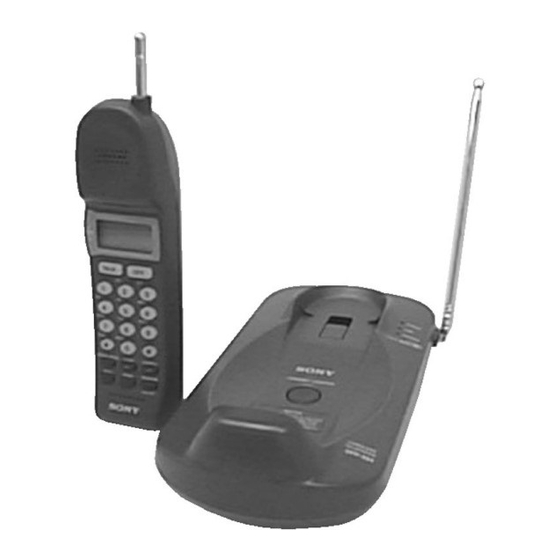
Handset
Photo: SPP-884
SPECIFICATIONS
Base unit
Power source
DC 9V from AC power adaptor
Rechargeable battery pack BP-T16
(SPP-884 only)
Battery charging time
Approx. 20 hours (SPP-884 only)
Dimensions
Approx. 120 × 64 × 223 mm (w/h/d),
antenna excluded
(approx. 4
Antenna: Approx. 680 mm
(approx. 26
Mass
Approx. 350 g (approx. 12 oz), wall
bracket and battery excluded
Design and specifications are subject to change without
notice.
• Abbreviation
E12 : 220–240V area of E model
E92 : 120V area of E model
– 1 –
Base unit
× 2
× 8
inches)
3/4
5/8
7/8
inches)
7/8
CORDLESS TELEPHONE
E Model
Advertisement
Table of Contents

Related Manuals for Sony SPP-874


Summary of Contents for Sony SPP-874
-
Page 1: Specifications
Approx. 120 × 64 × 223 mm (w/h/d), AC power adaptor (AC-T125) (1) (ARGENTINE) Telephone line cord (1) antenna excluded × 2 × 8 Rechargeable battery pack (BP-T16) (1) (SPP-874) (approx. 4 inches) Rechargeable battery pack (BP-T16) (2) (SPP-884) Antenna: Approx. 680 mm Wall bracket/stand (1) (approx. -
Page 2: Table Of Contents
COMPONENTS IDENTIFIED BY MARK ! OR DOTTED LINE WITH MARK ! ON THE SCHEMATIC DIAGRAMS AND IN THE PARTS LIST ARE CRITICAL TO SAFE OPERATION. REPLACE THESE COMPONENTS WITH SONY PARTS WHOSE PART NUMBERS APPEAR AS SHOWN IN THIS MANUAL OR IN SUPPLEMENTS PUBLISHED BY SONY. -
Page 3: General
SECTION 1 GENERAL This section is extracted from instruction manual. – 3 –... - Page 4 – 4 –...
- Page 5 – 5 –...
- Page 6 – 6 –...
- Page 7 – 7 –...
- Page 8 – 8 –...
-
Page 9: Disassembly
SECTION 2 DISASSEMBLY Note : Follow the disassembly procedure in the numerical order given. 2-1. CABINET (LOWER) 1 BTP 3x10 2 BTP 3x10 5 cabinet (lower) – 9 –... -
Page 10: Base Main Board
2-2. BASE MAIN BOARD 2 BVTP 2.6x8 1 BVTP 2.6x8 3 BASE MAIN board 4 telescopic antenna – 10 –... -
Page 11: Cabinet (Rear)
2-3. CABINET (REAR) 6 cabinet (rear) 1 battery lid 2 BVTP 2.6x10 5 claw 4 claws 3 claws 2-4. HAND MAIN BOARD 4 BVTP 2x8 5 unsolder 3 BVTP 2x8 6 HAND MAIN board 9 HAND KEY board 7 BVTP 2x8 2 CN3 0 terminal (antenna H) !£... -
Page 12: Testmode
SECTION 3 TEST MODE MACHINE TEST MODE BASE UNIT SECTION Set the Test Mode: 1. With the TEST I/O (TP808) terminal in “L” (low) input state, MANUAL TEST MODE cause Reset of Power ON. Equipment enters machine test mode. Set the Test Mode: 2. - Page 13 Channel Setting: During startup in machine test mode, make the following channel settings by loading the terminal input data. Pin No. TX frequency RX frequency TEST CLK/ COL4 COL3 COL2 COL1 (MHz) (MHz) Channel POWER LED (TP809) (TP807) (TP806) (TP805) (TP804) 43.720 48.760...
-
Page 14: Handset Section
HANDSET SECTION MACHINE TEST MODE Set the Test Mode: 1. When power on reset is applied while a “L” (low) is input the MANUAL TEST MODE TEST I/O (TP316) terminal (IC401 #§ pin), the RING (Level Set the Test Mode: H, 1 sec) sounds. - Page 15 Key Processing (Setting the Manual Test Mode) : DATA Light MUTE RSSI TEST POINT FUNCTION OUT- LCD HICUT SENS Light INITIAL – NORM TEST MODE TALK TP204 TP209 TX & RX – – – TP201 TP209 TEST MODE OFF – –...
- Page 16 Channel Setting: During startup in machine test mode, make the following channel settings by loading the terminal input data. Pin No. TX frequency RX frequency PC0-I/O PD3-I PD2-I PD1-I PD0-I (MHz) (MHz) Channel (TP205) (TP204) (TP203) (TP202) (TP201) 48.760 43.720 48.840 43.740 48.860...
-
Page 17: Electrical Adjustments
SECTION 4 ELECTRICAL ADJUSTMENTS BASE UNIT SECTION RX SECTION ADJUSTMENT RX DISCRI Adjustment Note: Note: • Apply 9V dc from regurated DC power supply. • Perform the adjustment at T3CH (28CH : 49.910 MHz) as a rule. • Perform the adjustment at T3CH (28CH : 49.910 MHz) as a rule. Setting : •... - Page 18 Adjustment Location : – base main board (component side) – RV501 FL501 L503 L602 RV601 – base main board (conductor side) – TP601 TP506 TP602 TP507 TP603 TP502 TP503 50 Ω TP505 TP508 TP702 TP701 – 18 –...
-
Page 19: Handset Section
RX DISCRI Adjustment HANDSET SECTION Adjustment Location : Note: • Perform the adjustment at T1CH (26CH : 43.780 MHz) as a rule. Note: – hand main board (side A) – Setting : • Apply 4V dc from regurated DC power supply. FM RF •... -
Page 20: Diagrams
SPP-874/884 SECTION 5 DIAGRAMS 5-1. BLOCK DIAGRAM — BASE SECTION — ANT1 TELESCOPIC ANTENNA FL501 RX DISCRI MIX, IF AMP, DET EXPANDER MJ701 IC501 ( 2/3 ) IC501 ( 1/3 ) LINE RECE CF501 T701 MIX IN 10.68MHz RF AMP... -
Page 21: Block Diagram -Handset Section
SPP-874/884 5-2. BLOCK DIAGRAM — HANDSET SECTION — ANT2 TELESCOPIC ANTENNA EXPANDER RX DISCRI MIX, IF AMP, DET IC1 ( 2/3 ) IC1 ( 1/3 ) RECE MIX IN 10.7MHz BPF1 EXPANDER 460kHz MUTE SPEAKER D-COMP VOLUME RSSI CONTROL LOCAL... -
Page 22: Printed Wiring Boards -Base Section
SPP-874/884 5-3. PRINTED WIRING BOARD — BASE SECTION — • Semiconductor Location Ref. No. Location D501 D502 D601 D701 D702 D703 D704 D706 D801 D804 D805 D806 D807 D808 D810 D841 D842 D901 C-10 D902 D903 D904 D908 D909 IC501... -
Page 23: Schematic Diagram -Base Section
SPP-874/884 5-4. SCHEMATIC DIAGRAM — BASE SECTION — • Refer to page 37 for IC Block Diagrams. Note: • All capacitors are in µF unless otherwise noted. pF: µµF 50 WV or less are not indicated except for electrolytics and tantalums. - Page 24 SPP-874/884 5-5. PRINTED WIRING BOARD — HAND MAIN SECTION — • Semiconductor Location Ref. No. Location D101 Q101 Q102 Q103 (Page 34) Note: • X : parts extracted from the component side. • Y : parts extracted from the conductor side.
-
Page 25: Schematic Diagram -Hand Main Section
SPP-874/884 5-6. SCHEMATIC DIAGRAM — HAND MAIN SECTION — • Refer to page 37 for IC Block Diagrams. (Page 36) Note: • All capacitors are in µF unless otherwise noted. pF: µµF 50 WV or less are not indicated except for electrolytics and tantalums. -
Page 26: Printed Wiring Boards -Hand Key Section
SPP-874/884 5-7. PRINTED WIRING BOARDS — HAND KEY SECTION — Note: • Abbreviation • X : parts extracted from the component side. : 220-240V area of E model • Y : parts extracted from the conductor side. : 120V area of E model •... -
Page 27: Schematic Diagram -Hand Key Section
SPP-874/884 5-8. SCHEMATIC DIAGRAM — HAND KEY SECTION — • Refer to page 37 for IC Block Diagrams. (Page 32) Note: • All capacitors are in µF unless otherwise noted. pF: µµF • Voltages are taken with a VOM (Input impedance 10 MΩ). -
Page 28: Ic Pin Descriptions
• IC Block Diagrams 5-9. IC PIN DESCRIPTIONS • IC801 LC6621108A (SYSTEM CONTROL) (BASE UNIT) Pin No. Pin Name Pin Description RSSI CTRL RSSI sens select output (L: Low sens) IC501 TB31224F (BASE MAIN BOARD) IC1 TB31224F (HAND MAIN BOARD) EEPROM DATA EEPROM data input/output (Not used in this set.) EEROM CLK... - Page 29 CHARGE DET Charge detection input (H: in charge) BAT-LOW-IN Battery low-voltage detection input — — Not used. (Fixed at L (SPP-874/884:E92), H (SPP-884:E12) in this set.) RX-DATA RF reception data input PLL-STB PLL control standby output PLL-DATA PLL control data output...
-
Page 30: Exploded Views
A-3672-503-A BASE MAIN BOARD, COMPLETE (SPP-884:E92) 7-685-134-19 SCREW +BTP 2.6X8 TYPE2 N-S A-3672-587-A BASE MAIN BOARD, COMPLETE (SPP-884:E12) 7-685-547-14 SCREW +BTP 3X10 TYPE2 N-S A-3672-596-A BASE MAIN BOARD, COMPLETE (SPP-874:E92) ANT1 1-501-982-11 ANTENNA, TELESCOPIC (BASE UNIT) A-3672-598-A BASE MAIN BOARD, COMPLETE (SPP-874:E12) -
Page 31: Handset Section
7-685-535-14 SCREW +BTP 2.6X10 TYPE2 N-S * 58 A-3622-241-A HAND KEY BOARD, COMPLETE (SPP-884:E12) 3-027-147-01 SHEET (RECEIVER), ADHESIVE * 58 A-3622-245-A HAND KEY BOARD, COMPLETE (SPP-874:E92) 3-027-565-01 SHEET (LCD), ELECTROSTATIC * 58 A-3622-247-A HAND KEY BOARD, COMPLETE (SPP-874:E12) * 73... -
Page 32: Electrical Parts List
A-3672-503-A BASE MAIN BOARD, COMPLETE (SPP-884:E92) C534 1-126-964-11 ELECT 10uF A-3672-587-A BASE MAIN BOARD, COMPLETE (SPP-884:E12) C535 1-163-038-00 CERAMIC CHIP 0.1uF A-3672-596-A BASE MAIN BOARD, COMPLETE (SPP-874:E92) C536 1-163-234-11 CERAMIC CHIP 20PF A-3672-598-A BASE MAIN BOARD, COMPLETE (SPP-874:E12) C537 1-163-021-11 CERAMIC CHIP 0.01uF... - Page 33 8-719-991-33 DIODE 1SS133T-77 L501 1-414-141-11 INDUCTOR 0.82uH D706 8-719-049-07 LED SLR-342MG3F (LINE) L502 1-410-992-11 INDUCTOR CHIP 0.82uH D801 8-719-988-62 DIODE 1SS355 (SPP-874,SPP-884:E12) D804 8-719-988-62 DIODE 1SS355 (E12) L502 1-410-992-42 INDUCTOR CHIP 0.82uH (SPP-884:E92) L503 1-409-798-11 COIL, OSC D805 8-719-988-62Å DIODE 1SS355 L601...
- Page 34 BASE MAIN Ref. No. Part No. Description Remark Ref. No. Part No. Description Remark < TRANSISTOR > R607 1-216-049-11 RES,CHIP 1/10W R608 1-216-113-00 METAL CHIP 470K 1/10W Q501 8-729-031-86 TRANSISTOR 2SC3142-J3J4-TB R609 1-216-085-00 METAL CHIP 1/10W Q601 8-729-031-85 TRANSISTOR 2SC4365-34-TB R610 1-216-073-00 METAL CHIP 1/10W...
- Page 35 A-3622-241-A HAND KEY BOARD, COMPLETE (SPP-884:E12) D401 8-719-914-43 DIODE DAN202K (INCLUDING SUB BOARD, COMPLETE) D402 8-719-058-24 DIODE RB501V-40TE-17 A-3622-245-A HAND KEY BOARD, COMPLETE (SPP-874:E92) D403 8-719-914-43 DIODE DAN202K (INCLUDING SUB BOARD, COMPLETE) D404 8-719-938-75 DIODE SB05-05CP A-3622-247-A HAND KEY BOARD, COMPLETE (SPP-874:E12) (INCLUDING SUB BOARD, COMPLETE) <...
- Page 36 8-729-216-22 TRANSISTOR 2SA1162-G R324 1-216-097-00 RES,CHIP 100K 1/10W Q404 8-729-120-28 TRANSISTOR 2SC1623-L5L6 R326 1-216-295-00 SHORT Q405 8-729-216-22 TRANSISTOR 2SA1162-G R327 1-216-295-00 SHORT (SPP-874:E12) R328 1-216-295-00 SHORT (SPP-874:E92,SPP-884) < RESISTOR > R329 1-216-073-00 METAL CHIP 1/10W R205 1-216-097-00 RES,CHIP 100K 1/10W R330...
- Page 37 1-163-021-11 CERAMIC CHIP 0.01uF 1-163-021-11 CERAMIC CHIP 0.01uF 1-766-180-11 PIN, CONNECTOR (PC BOARD) 2P 1-163-021-11 CERAMIC CHIP 0.01uF 1-785-414-11 CONNECTOR, FFC/FPC 15P (SPP-874,SPP-884:E12) < DISCHARGE GAP > 1-164-346-11 CERAMIC CHIP 1-163-038-00 CERAMIC CHIP 0.1uF CP101 1-519-504-11 GAP, DISCHARGE 1-163-809-11 CERAMIC CHIP 0.047uF...
- Page 38 1/10W 1-216-057-00 METAL CHIP 2.2K 1/10W 1-771-405-11 SWITCH, RUBBER KEY (SPP-884) 1-216-061-00 METAL CHIP 3.3K 1/10W 1-771-405-31 SWITCH, RUBBER KEY (SPP-874) 1-216-049-11 RES,CHIP 1/10W 1-790-013-11 WIRE (FLAT TYPE) (15 CORE) ANT1 1-501-982-11 ANTENNA, TELESCOPIC (BASE UNIT) 1-216-097-00 RES,CHIP 100K 1/10W...