Table of Contents
Advertisement
DVD-VCR Player
Contents
Chapter
Sec. 1:
Adjustment Procedure
Schematic Diagrams and CBA's
Exploded Views
Mechanical and Electrical Parts Lists
Sec. 2: Standard Maintenance
Mechanism Alignment Procedures
Disassembly / Assembly of Mechanism
Deck Exploded Views
Sec. 3: Spare Parts List
Revision List
©
Copyright 2003 Philips Consumer Electronics B.V. Eindhoven, The Netherlands.
All rights reserved. No part of this publication may be reproduced, stored in a
retrieval system or transmitted, in any form or by any means, electronic,
mechanical, photocopying, or otherwise without the prior permission of Philips.
Published by MW 0366 Service PaCE
Survey of versions:
/00
/05
/02
Printed in the Netherlands
PAL I
PAL B/G
PAL B/G,L,L' & SECAM B/G,L,L'
Subject to modification
DVD757VR
DVD757VR /00
DVD757VR /02
DVD757VR /05
EN 3122 785 13771
Advertisement
Chapters
Table of Contents

Related Manuals for Philips DVD757VR /00


Summary of Contents for Philips DVD757VR /00
- Page 1 All rights reserved. No part of this publication may be reproduced, stored in a retrieval system or transmitted, in any form or by any means, electronic, mechanical, photocopying, or otherwise without the prior permission of Philips. Published by MW 0366 Service PaCE...
-
Page 2: Table Of Contents
MAIN SECTION DIGITAL VIDEO DISC PLAYER & VIDEO CASSETTE RECORDER Sec. 1: Main Section I Adjustment Procedures I Schematic Diagrams and CBA’s I Exploded Views I Mechanical and Electrical Parts List TABLE OF CONTENTS LASER BEAM SAFETY PRECAUTIONS ........... . . 1-1-1 IMPORTANT SAFETY PRECAUTIONS . -
Page 3: Laser Beam Safety Precautions
LASER BEAM SAFETY PRECAUTIONS This DVD player uses a pickup that emits a laser beam. Do not look directly at the laser beam coming from the pickup or allow it to strike against your skin. The laser beam is emitted from the location shown in the figure. When checking the laser diode, be sure to keep your eyes at least 30cm away from the pickup lens when the diode is turned on. -
Page 4: Important Safety Precautions
IMPORTANT SAFETY PRECAUTIONS Product Safety Notice I. Also check areas surrounding repaired locations. J. Use care that foreign objects (screws, solder drop- Some electrical and mechanical parts have special lets, etc.) do not remain inside the set. safety-related characteristics which are often not evi- K. -
Page 5: Safety Check After Servicing
Safety Check after Servicing Chassis or Secondary Conductor Examine the area surrounding the repaired location for damage or deterioration. Observe that screws, parts, and wires have been returned to their original posi- Primary Circuit Terminals tions. Afterwards, do the following tests and confirm the specified values to verify compliance with safety standards. -
Page 6: Standard Notes For Servicing
STANDARD NOTES FOR SERVICING Circuit Board Indications How to Remove / Install Flat Pack-IC a. The output pin of the 3 pin Regulator ICs is indi- 1. Removal cated as shown. With Hot-Air Flat Pack-IC Desoldering Machine:. (1) Prepare the hot-air flat pack-IC desoldering Top View Bottom View machine, then apply hot air to the Flat Pack-IC... - Page 7 With Soldering Iron: (4) Bottom of the flat pack-IC is fixed with glue to the CBA; when removing entire flat pack-IC, first apply (1) Using desoldering braid, remove the solder from all soldering iron to center of the flat pack-IC and heat pins of the flat pack-IC.
- Page 8 2. Installation Instructions for Handling Semi-conductors (1) Using desoldering braid, remove the solder from the foil of each pin of the flat pack-IC on the CBA so Electrostatic breakdown of the semi-conductors may you can install a replacement flat pack-IC more occur due to a potential difference caused by electro- easily.
-
Page 9: Preparation For Servicing
PREPARATION FOR SERVICING How to Enter the Service Mode About Optical Sensors Caution: An optical sensor system is used for the Tape Start and End Sensors on this equipment. Carefully read and follow the instructions below. Otherwise the unit may operate erratically. What to do for preparation Insert a tape into the Deck Mechanism Assembly and press the PLAY button. -
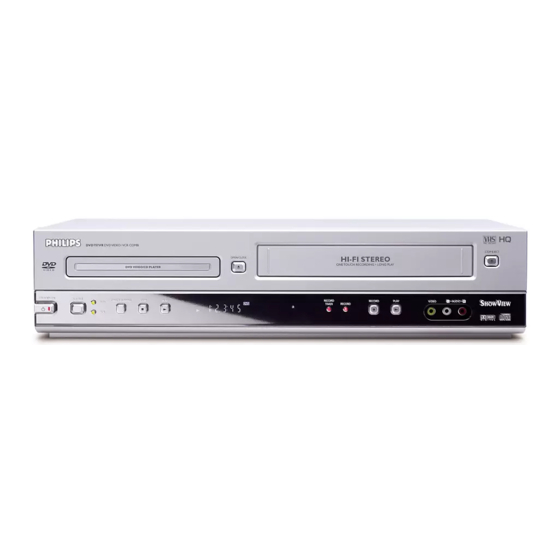
Page 10: Operating Controls And Functions
OPERATING CONTROLS AND FUNCTIONS [ DVD757VR/00 ] 1-5-1 H9520IB... - Page 11 1-5-2 H9520IB...
- Page 12 [ DVD757VR/05 ] 1-5-3 H9520IB...
- Page 13 1-5-4 H9520IB...
-
Page 14: Front Panel
[ DVD757VR/02 ] 15. VCR light (VCR) Front Panel light appears when DVD/VCR in VCR mode 16. SOURCE button (DVD,VCR) to select between DVD and VCR mode 17. ySTANDBY-ON button (DVD,VCR) OPEN/CLOSE to switch the player to ON or OFF STANDBY-ON light (DVD,VCR) STANDBY-ON SOURCE... - Page 15 1-5-6 H9520IB...
-
Page 16: Signal Name Abbreviations
SIGNAL NAME ABBREVIATIONS Signal Name Function Signal Name Function Color Phase Rotary Changeover C-ROTA SIgnal SCART 1 8Pin Output Control 8POUT-1 Signal C-SYNC Composite Synchronized Pulse Control SCART 1 8Pin Level by 8POUT-2 CLKSEL Clock Select (GND) using 8POUT-1 and 8POUT-2 SECAM or MESECAM Chroma A-COM Audio Head Common... - Page 17 Signal Name Function Signal Name Function DVD Component Video Signal N-A-REC Normal Audio Recording DVD-R-OUT (red) Oscillator Input DVD-VIDEO DVD Video Control Signal Clock Input OSCin END-S Tape End Position Detect Signal for letter size FE-H GND Ground for Full Erase Head OSCout Clock Output for letter size Frequency Characteristics...
- Page 18 Signal Name Function TIMER+5V +5V at Timer TIMER- LED “TIMER” LED Signal Output Special Playback = “H” in SECAM TRICK-H Mode TU-AUDIO Tuner Audio Input Signal TU-VIDEO Tuner Video Input Signal Video Envelope Comparator V-ENV Signal V-IN Video Signal Input V-OUT Video Signal Output VCR LED...
-
Page 19: Cabinet Disassembly Instructions
CABINET DISASSEMBLY INSTRUCTIONS 1. Disassembly Flowchart REMOVAL REMOVE/*UNHOOK/ This flowchart indicates the disassembly steps to gain LOC. PART Fig. UNLOCK/RELEASE/ Note access to item(s) to be serviced. When reassembling, UNPLUG/DESOLDER follow the steps in reverse order. Bend, route, and dress the cables as they were originally. 3(S-9) Bracket [1] Top Cover... - Page 20 Reference Notes (S-3) CAUTION 1: Locking Tabs (L-1) are fragile. Be careful (S-3A) not to break them. [3] Top Bracket 1-1. Remove Screw (S-2). 1-2. Release seven Locking Tabs (L-1) (to do this, first release five Locking Tabs (A) at the side and (S-3A) top, and then release two Locking Tabs (B) at the (L-1)
- Page 21 (S-5) CN201 (S-9) (S-5) [5] DVD Main (S-8A) CN301 [9] Rear Panel (S-8) [8] PCB Bracket [7] Power Supply CBA (S-8) (S-8A) DVD Mecha Fig. D6 Short the three short (S-11) (S-10) lands by soldering (S-10) (S-11A) Slide (S-11) (S-10) (S-11A) Pickup Unit View for A...
- Page 22 FE Head Cylinder Assembly [11] Deck ACE Head Assembly Assembly SW507 LD-SW [12] Main CBA [12] Main CBA [15] Jack CBA [11] Deck Assembly [16] Front CBA Cam Gear CN651 Hole Shaft Hole LD-SW [12] Main CBA [13] DVD OPEN/ Lead with blue stripe CLOSE CBA Desolder from bottom...
- Page 23 (S-13) [17] Deck Pedestal (S-13) (S-14) [18] Side Bracket Fig. D9 To Remove the Disc Manually 1. Remove the Top Cover. 2. Rotate this roulette in the direction of the arrow as shown below. Top Cover DVD Mecha Tray Deck Assembly Rotate this roulette in the direction of the arrow 1-7-5...
-
Page 24: Electrical Adjustment Instructions
ELECTRICAL ADJUSTMENT INSTRUCTIONS General Note: "CBA" is an abbreviation for "Circuit Board Assembly." NOTE: Figure 1 1.Electrical adjustments are required after replacing circuit components and certain mechanical parts. It is important to do these adjustments only after EXT. Syncronize Trigger Point all repairs and replacements have been com- pleted. -
Page 25: Firmware Renewal Mode
FIRMWARE RENEWAL MODE 1. Turn the power on and remove the disc on the tray. 5. After programming is finished, the tray opens auto- 2. To put the DVD player into version up mode, press matically. Fig. e appears on the screen and the [9], [8], [7], [6], and [SEARCH MODE] buttons on checksum in (*3) of Fig. -
Page 26: Block Diagrams
BLOCK DIAGRAMS Servo/System Control Block Diagram Comparison Chart of Models & Marks NOTE FOR WIRE CONNECTORS: TEST POINT INFORMATION Model Mark " " = SMD 1. PREFIX SYMBOL "CN" MEANS CONNECTOR. :INDICATES A TEST POINT WITH A JUMPER WIRE ACROSS A HOLE IN THE PCB. (CAN DISCONNECT AND RECONNECT.) :USED TO INDICATE A TEST POINT WITH A COMPONENT LEAD ON FOIL SIDE. - Page 27 Video Block Diagram Comparison Chart of Models & Marks NOTE FOR WIRE CONNECTORS: TEST POINT INFORMATION :INDICATES A TEST POINT WITH A JUMPER WIRE ACROSS A HOLE IN THE PCB. 1. PREFIX SYMBOL "CN" MEANS CONNECTOR. (CAN DISCONNECT AND RECONNECT.) :USED TO INDICATE A TEST POINT WITH A COMPONENT LEAD ON FOIL SIDE.
- Page 28 Audio Block Diagram NOTE FOR WIRE CONNECTORS: " " = SMD 1. PREFIX SYMBOL "CN" MEANS CONNECTOR. (CAN DISCONNECT AND RECONNECT.) 2. PREFIX SYMBOL "CL" MEANS WIRE-SOLDER HOLES OF THE PCB. (WIRE IS SOLDERED DIRECTLY.) PB-AUDIO SIGNAL REC-AUDIO SIGNAL Mode : SP/REC MAIN CBA N-A-PB TO Hi-Fi...
- Page 29 Hi-Fi Audio Block Diagram Comparison Chart of Models & Marks NOTE FOR WIRE CONNECTORS: 1. PREFIX SYMBOL "CN" MEANS CONNECTOR. " " = SMD Model Mark (CAN DISCONNECT AND RECONNECT.) 2. PREFIX SYMBOL "CL" MEANS WIRE-SOLDER DVD757VR/00 HOLES OF THE PCB. (WIRE IS SOLDERED DIRECTLY.) DVD AUDIO SIGNAL DVD757VR/05...
- Page 30 Power Supply Block Diagram NOTE : CAUTION CAUTION ! FOR CONTINUED PROTECTION AGAINST FIRE HAZARD, Fixed voltage (or Auto voltage selectable ) power supply circuit is used in this unit. The voltage for parts in hot circuit is measured using If Main Fuse (F001) is blown, check to see that all components in the power supply REPLACE ONLY WITH THE SAME TYPE T1.6AL/250V FUSE.
- Page 31 DVD System Control/Servo Block Diagram NOTE FOR WIRE CONNECTORS: " " = SMD 1. PREFIX SYMBOL "CN" MEANS CONNECTOR. (CAN DISCONNECT AND RECONNECT.) 2. PREFIX SYMBOL "CL" MEANS WIRE-SOLDER HOLES OF THE PCB. (WIRE IS SOLDERED DIRECTLY.) FOCUS SERVO SIGNAL TRACKING SERVO SIGNAL SLED SERVO SIGNAL SPINDLE SERVO SIGNAL...
- Page 32 Digital Signal Process Block Diagram DATA(AUDIO) SIGNAL DATA(VIDEO/AUDIO) SIGNAL DVD VIDEO SIGNAL " " = SMD IC102 (SDRAM) IC101 (MICRO CONTROLLER) NOTE FOR WIRE CONNECTORS: 1. PREFIX SYMBOL "CN" MEANS CONNECTOR. (CAN DISCONNECT AND RECONNECT.) 2. PREFIX SYMBOL "CL" MEANS WIRE-SOLDER SDRAM ADDRESS(0-10) SDRAM ADDRESS(0-10) HOLES OF THE PCB.
- Page 33 DVD Video / Audio Block Diagram DVD VIDEO SIGNAL DATA(AUDIO) SIGNAL DVD AUDIO SIGNAL " " = SMD NOTE FOR WIRE CONNECTORS: 1. PREFIX SYMBOL "CN" MEANS CONNECTOR. (CAN DISCONNECT AND RECONNECT.) 2. PREFIX SYMBOL "CL" MEANS WIRE-SOLDER HOLES OF THE PCB. IC1402 (VIDEO DRIVER) (WIRE IS SOLDERED DIRECTLY.) DRIVER...
-
Page 34: Schematic Diagrams / Cba's And Test Points
SCHEMATIC DIAGRAMS / CBA'S AND TEST POINTS Standard Notes Notes: WARNING 1. Do not use the part number shown on these draw- ings for ordering. The correct part number is Many electrical and mechanical parts in this chassis shown in the parts list, and may be slightly different have special characteristics. - Page 35 Main 1/11 Schematic Diagram Parts Location Guide Ref No. Position Ref No. Position Ref No. Position CONNECTORS CAPACITORS RESISTORS C505 CL502 R550 C506 CL504 R551 C508 DIODES R552 C509 D510 R555 C510 D511 R558 C511 D512 R560 C513 D555 R565 C514 R567 C515...
- Page 36 Main 1/11 Schematic Diagram < VCR Section > Comparison Chart of IC501 KEY VOLTAGE CHART PLAY MODE Models and Marks KEY 1 (7 PIN) KEY 2 (8 PIN) “ “ = SMD REC MODE MODEL MARK 0.00 ~ 0.51V REC/OTR ------------------- (2.5) DVD MODE...
- Page 37 Main 2/11 Schematic Diagram < VCR Section > FL2001 MATRIX CHART PLAY MODE Note: “ “ = SMD REC MODE When it is necessary to replace one or more of the following Diodes, STANDBY (2.5) DVD MODE all one should be replaced: D501, D504. REPEAT <5.0>...
- Page 38 Main 2/11 Schematic Diagram Parts Location Guide Ref No. Position Ref No. Position CAPACITORS RESISTORS C611 R501 C612 R511 C614 R514 C615 R516 C701 R519 C703 R520 C706 R522 C708 R523 C709 R525 C711 R526 C712 R528 R529 C714 C715 R530 C716 R531...
- Page 39 Main 3/11 Schematic Diagram Parts Location Guide Ref No. Position Ref No. Position Ref No. Position Ref No. Position CAPACITORS CAPACITORS TRANSISTORS RESISTORS C251 C346 Q301 R337 C252 C347 Q302 R339 C253 C348 Q401 R401 C254 C349 Q403 R402 C301 C350 Q404 R404...
- Page 40 Main 3/11 Schematic Diagram < VCR Section > Comparison Chart of “ “ = SMD PLAY MODE Models and Marks REC MODE (2.5) DVD MODE MODEL MARK <5.0> THE SAME VOLTAGE FOR BOTH DVD757VR/00 INDICATES THAT THE VOLTAGE PLAY, REC & DVD MODES. DVD757VR/05 IS NOT CONSISTENT HERE.
- Page 41 Main 4/11 Schematic Diagram < VCR Section > “ “ = SMD PLAY MODE REC MODE (2.5) DVD MODE <5.0> THE SAME VOLTAGE FOR BOTH INDICATES THAT THE VOLTAGE PLAY, REC & DVD MODES. IS NOT CONSISTENT HERE. 1-11-11 1-11-12 H9520SCM4...
- Page 42 Main 4/11 Schematic Diagram Parts Location Guide Ref No. Position Ref No. Position CAPACITORS COILS C451 L451 C452 L452 C453 RESISTORS C454 R451 C455 R452 C456 R453 C457 R454 C458 R455 C461 R456 C462 R457 C463 R458 R459 C464 C465 R460 C466 R461...
- Page 43 Main 5/11 Schematic Diagram Parts Location Guide Ref No. Position Ref No. Position Ref No. Position CONNECTORS CAPACITORS RESISTORS C1201 CN1601 R1225 C1202 DIODES R1226 C1205 D1301 R1227 C1206 D1401 AA-2 R1228 C1207 D1402 AA-2 R1235 C1208 D1501 AB-3 R1236 C1221 R1237 C1222...
- Page 44 Main 5/11 Schematic Diagram < VCR Section > PLAY MODE “ “ = SMD REC MODE (2.5) DVD MODE <5.0> THE SAME VOLTAGE FOR BOTH INDICATES THAT THE VOLTAGE PLAY, REC & DVD MODES. IS NOT CONSISTENT HERE. 1-11-15 1-11-16 H9520SCM5...
- Page 45 Main 6/11 Schematic Diagram < VCR Section > PLAY MODE “ “ = SMD REC MODE (2.5) DVD MODE <5.0> THE SAME VOLTAGE FOR BOTH INDICATES THAT THE VOLTAGE PLAY, REC & DVD MODES. IS NOT CONSISTENT HERE. MAIN 6/11 Schematic Diagram Parts Location Guide Ref No.
- Page 46 Main 7/11 Schematic Diagram < VCR Section > Comparison Chart of MAIN 7/11 Schematic Diagram Models and Marks “ “ = SMD PLAY MODE Parts Location Guide MODEL MARK REC MODE Ref No. Position DVD757VR/00 (2.5) DVD MODE CAPACITORS <5.0> DVD757VR/05 THE SAME VOLTAGE FOR BOTH C104...
- Page 47 Main 8/11 Schematic Diagram < VCR Section > PLAY MODE “ “ = SMD REC MODE (2.5) DVD MODE <5.0> THE SAME VOLTAGE FOR BOTH INDICATES THAT THE VOLTAGE PLAY, REC & DVD MODES. IS NOT CONSISTENT HERE. 1-11-21 1-11-22 H9520SCM8...
- Page 48 Main 8/11 Schematic Diagram Parts Location Guide Ref No. Position CAPACITORS C2004 AP-1 C2008 AO-3 C2009 AO-3 C2012 AQ-1 CONNECTORS CL2015 AM-4 DIODES D2009 AO-3 TRANSISTORS Q1505 AN-2 Q1506 AO-2 Q2007 AO-4 RESISTORS R2005 AP-1 R2022 AN-2 R2027 AO-3 R2038 AO-4 R2039 AO-4...
- Page 49 Main 9/11 Schematic Diagram Parts Location Guide Ref No. Position Ref No. Position CAPACITORS TRANSISTORS C056 AU-4 Q057 AU-3 C057 AU-3 Q058 AT-3 C058 AU-3 Q059 AT-3 C059 AU-3 Q1052 AT-1 C060 AU-3 Q1053 AS-1 C062 AU-3 Q1054 AS-1 C063 AU-3 Q1055 AU-2...
- Page 50 Main 9/11 Schematic Diagram < VCR Section > PLAY MODE “ “ = SMD REC MODE (2.5) DVD MODE <5.0> THE SAME VOLTAGE FOR BOTH INDICATES THAT THE VOLTAGE PLAY, REC & DVD MODES. IS NOT CONSISTENT HERE. 1-11-25 1-11-26 H9520SCM9...
- Page 51 Main 10/11 Schematic Diagram < VCR Section > PLAY MODE “ “ = SMD REC MODE (2.5) DVD MODE <5.0> THE SAME VOLTAGE FOR BOTH INDICATES THAT THE VOLTAGE PLAY, REC & DVD MODES. IS NOT CONSISTENT HERE. MAIN10/11 Schematic Diagram Parts Location Guide Ref No.
- Page 52 Main 11/11 Schematic Diagram ( C ) < VCR Section > Comparison Chart of Models and Marks MODEL MARK DVD757VR/00 DVD757VR/05 DVD757VR/02 PLAY MODE “ “ = SMD REC MODE (2.5) DVD MODE <5.0> THE SAME VOLTAGE FOR BOTH INDICATES THAT THE VOLTAGE PLAY, REC &...
- Page 53 Main CBA Top View Sensor CBA Top View BHB300F01014-A TP301 TP751 BHB300F01014-B C-PB V-OUT VR501 SW-P TP503 TP504 RF-SW TP501 S-INH 1-11-31 1-11-32 BH9520F01012A...
- Page 54 Main CBA Bottom View 1-11-33 1-11-34 BH9520F01012A...
- Page 55 Main CBA Parts Location Guide Ref No. Position Ref No. Position Ref No. Position Ref No. Position Ref No. Position Ref No. Position Ref No. Position Ref No. Position Ref No. Position Ref No. Position Ref No. Position Ref No. Position CAPACITORS CAPACITORS...
- Page 56 Function CBA Top View Function CBA Bottom View BH9520F01012B DVD OPEN/CLOSE CBA Top View DVD OPEN /CLOSE CBA Bottom View BH9520F01012C 1-11-37 1-11-38...
- Page 57 Power Supply Schematic Diagram < VCR Section > CAUTION ! CAUTION ! PLAY MODE “ “ = SMD For continued protection against fire hazard, Fixed voltage ( or Auto voltage selectable ) power supply circuit is used in this unit. REC MODE replace only with the same type fuse.
- Page 58 Power Supply CBA Parts Location Guide Power Supply Schematic Diagram Parts Location Guide Ref No. Position Ref No. Position Ref No. Position Ref No. Position Ref No. Position Ref No. Position CAPACITORS DIODES RESISTORS CAPACITORS DIODES RESISTORS C013 D1002 R068 C013 D1002 R068...
- Page 59 Power Supply CBA Top View Power Supply CBA Bottom View BECAUSE A HOT CHASSIS GROUND IS PRESENT IN THE POWER CAUTION ! CAUTION ! SUPPLY CIRCUIT , AN ISOLATION TRANSFORMER MUST BE USED. For continued protection against fire hazard, Fixed voltage ( or Auto voltage selectable ) power supply circuit is used in this unit. ALSO , IN ORDER TO HAVE THE ABILITY TO INCREASE THE INPUT replace only with the same type fuse.
- Page 60 Front Schematic Diagram Note: When it is necessary to replace one or more of the following Diodes, all one should be replaced: D651, D652, D653. FRONT Schematic Diagram Parts Location Guide Ref No. Position CONNECTORS CN651 DIODES D651 D652 D653 RESISTORS R651 R652...
- Page 61 Jack Schematic Diagram JACK Schematic Diagram JACK CBA Parts Location Guide Parts Location Guide Ref No. Position Ref No. Position CAPACITORS CAPACITORS C101 C101 C102 C102 C105 C105 C106 C106 C108 C108 C110 C110 C111 C111 C119 C119 CONNECTORS CONNECTORS CL2018 CL2018 DIODES...
- Page 62 AFV Schematic Diagram Comparison Chart of Models and Marks MODEL MARK AFV Schematic Diagram Parts Location Guide DVD757VR/00 Ref No. Position Ref No. Position DVD757VR/05 CONNECTORS CAPACITORS DVD757VR/02 DIODES COILS RESISTORS CRYSTAL OSCILLATORS AFV CBA Top View AFV CBA Bottom View AFV CBA Parts Location Guide Ref No.
- Page 63 DVD Main 1/3 Schematic Diagram < DVD Section > PLAY MODE “ “ = SMD STOP MODE (2.5) THE SAME VOLTAGE FOR INDICATES THAT THE VOLTAGE BOTH PLAY & STOP MODES. IS NOT CONSISTENT HERE. 1-11-51 1-11-52 H9520SCD1...
- Page 64 DVD Main 2/3 Schematic Diagram < DVD Section > PLAY MODE “ “ = SMD STOP MODE (2.5) THE SAME VOLTAGE FOR INDICATES THAT THE VOLTAGE BOTH PLAY & STOP MODES. IS NOT CONSISTENT HERE. 1-11-53 1-11-54 H9520SCD2...
- Page 65 IC101 VOLTAGE CHART PIN.NO PLAY STOP PIN.NO PLAY STOP PIN.NO PLAY STOP PIN.NO PLAY STOP PIN.NO PLAY STOP PIN.NO PLAY STOP PIN.NO PLAY STOP PIN.NO PLAY STOP ----- ----- ----- ----- ----- ----- ----- ----- ----- ----- ----- ----- ----- ----- ----- -----...
- Page 66 DVD Main 3/3 Schematic Diagram < DVD Section > PLAY MODE “ “ = SMD STOP MODE (2.5) THE SAME VOLTAGE FOR INDICATES THAT THE VOLTAGE BOTH PLAY & STOP MODES. IS NOT CONSISTENT HERE. 1-11-57 1-11-58 H9520SCD3...
-
Page 67: Waveforms
WAVEFORMS (TP301 of Main CBA) UPPER (TP504 of Main CBA) LOWER C-PB 10mV x 10 RF-SW 0.5V x 10 5msec (TP751 of Main CBA) UPPER (TP504 of Main CBA) LOWER V-OUT 0.1V x 10 RF-SW 0.5V x 10 50usec (TP751 of Main CBA) V-OUT E-E 10usec 50mV x 10... - Page 68 WAVEFORMS NOTE: Input CD: 1kHz PLAY (WF7~WF9) DVD: POWER ON (STOP) MODE (WF4~WF6) Pin 1 of CN1601 Pin 13 of CN1601 AUDIO-L 0.5msec VIDEO-Y 0.2V 20µsec Pin 9 of CN1601 Pin 15 of CN1601 VIDEO-C 0.2V 20µsec AUDIO-R Pin 31 of IC1402 Pin 18 of CN1601 VIDEO-CVBS 0.5V...
-
Page 69: Wiring Diagram
WIRING DIAGRAM < VCR SECTION > NOTE FOR WIRE CONNECTORS: FRONT REAR 1. PREFIX SYMBOL "CN" MEANS CONNECTOR. (CAN DISCONNECT AND RECONNECT.) VIDEO AUDIO AUDIO S-VIDEO DIGITAL AUDIO AUDIO 2. PREFIX SYMBOL "CL" MEANS WIRE-SOLDER OUT(R) OUT (L) AUDIO OUT OUT (R) OUT (L) ANT-IN... - Page 70 WIRING DIAGRAM < DVD SECTION > NOTE FOR WIRE CONNECTORS: 1. PREFIX SYMBOL "CN" MEANS CONNECTOR. (CAN DISCONNECT AND RECONNECT.) 2. PREFIX SYMBOL "CL" MEANS WIRE-SOLDER HOLES OF THE PCB. (WIRE IS SOLDERED DIRECTLY.) DVD MECHANISM CN401 EV+1.5V EV+1.5V SENSOR EV+1.5V TRAY-OUT EV+3.3V...
-
Page 71: System Control Timing Charts
SYSTEM CONTROL TIMING CHARTS [ VCR Section ] Mode SW : LD-SW LD-SW Position detection A/D Input voltage Limit Symbol (Calculated voltage) 3.76V~4.50V (4.12V) 4.51V~5.00V (5.00V) 0.00V~0.25V (0.00V) 1.06V~1.50V (1.21V) 0.66V~1.05V (0.91V) 1.99V~2.60V (2.17V) 1.51V~1.98V (1.80V) 3.20V~3.75V (3.40V) 0.26V~0.65V (0.44V) 4.51V~5.00V (5.00V) 2.61V~3.19V... - Page 72 Still/Slow Control Frame Advance Timing Chart 1) SP Mode 18 RF-SW The first rise of RF-SW after a rise in F-AD signal F-AD (Internal Signal) "H" "H" "Z" C-DRIVE "L" "L" Stop detection (T2) Acceleration Detection (T1) Slow Tracking Value PB CTL Reversal Limit Value 20ms...
- Page 73 2) LP/SLP Mode 18 RF-SW The first rise of RF-SW after a rise in F-AD signal F-AD (Internal Signal) "H" "H" "Z" C-DRIVE "L" "L" Stop detection (T2) Acceleration Detection (T1) Slow Tracking Value PB CTL Reversal Limit Value 20ms 78 C-F/R 16 H-A-SW 15 ROTA...
- Page 74 EJECT ST-S/ END-S "OFF" CASS.LOAD LD-FWD 0.2s LD-REV 0.7s LD-FWD 0.4s LD-FWD 0.5s LD-REV STOP(A) PLAY LD-FWD PLAY LD-FWD LD-REV 0.2s LD-FWD PLAY PLAY PAUSE (SLOW) LD-FWD STILL(SLOW) PLAY LD-REV 0.2s LD-FWD PLAY STOP /EJECT LD-REV STOP(A) Fig. 3 1-14-4 H9520TI...
- Page 75 STOP(A) STOP LD-REV 0.2s LD-FWD STOP /EJECT LD-FWD 2.5s LD-FWD 0.5s LD-REV STOP(A) LD-REV 0.2s LD-FWD STOP /EJECT LD-FWD 2.5s LD-FWD 0.5s LD-REV STOP(A) LD-FWD PAUSE LD-FWD 2.5s Short REV LD-REV 0.2s LD-FWD REC PAUSE REC or PAUSE STOP /EJECT LD-FWD 1.0s LD-REV...
-
Page 76: Dvd Section
[ DVD Section ] Tray Close ~ Play / Play ~ Tray Open Disc Tray Tray Disc Stop Open Close Rotation Play 3.3V Tray OUT (TL220) 3.3V Tray IN (TL221) 1.65V Sled Drive (TP303) 1.65V Disc Drive (TP301) 1.65V Focus Drive (TP304) 1.65V Tracking Drive... -
Page 77: Ic Pin Function Descriptions
IC PIN FUNCTION DESCRIPTIONS [ VCR Section ] Signal Active Mark Function Name Level Comparison Chart of Models and Marks Video Head OUT RF-SW Switching Pulse Model Mark OUT Hi-Fi-H- HiFi Audio Head DVD757VR/00 Switching Pulse DVD757VR/05 VPS/PDC Data IN DAVN-L Receive = “L”... - Page 78 Signal Active Signal Active Mark Function Mark Function Name Level Name Level Clock Output for OUT IIC-BUS- IIC BUS Control OUT OSCout letter size Clock Not Used IIC-BUS- IIC BUS Control Data Not Used OUT P-OFF-H Power Off at High IN FSC-IN 4.43MHz Clock OUT OUTPUT-...
- Page 79 IC621 [ PT6315-S(TP) ] Signal Active Mark Function Name Level Signal Playback/Record In/Out Name Function CTL + Name Control Signal (+) Clock Input CTL AMP AMPC Connected Serial Interface Strobe Terminal CTLAMP To Monitor for CTL Key Data 1 Input PULSE AMP Output Key Data 2 Input...
-
Page 80: Lead Identifications
LEAD IDENTIFICATIONS BN1L3Z(P) 2SC1815-BL(TPE2) MID-32A22 BN1F4M-T PQ070XF01SZ PT204-6B-12 BN1L4M-T 2SC1815-Y(TPE2) BA1F4M-T 2SC1815-GR(TPE2) KTA1266(GR) 2SC2120-Y(TPE2) KTC3199(Y,GR,BL) KTC3203(Y) 2SC2785(J,H,F,K) 2SA1015-GR(TPE2) KRC103M 2SA1020(Y) 2SC3266-Y(TPE2) KRA103M 2SA1175(J,H,F) KTA1281(Y) KTA1267(Y) KTC3205(Y) 1 2 3 4 KTA1267(GR) KTC3198(Y,GR) KRA104M KIA339F EL E C B KRA110M FA1F4M-T1B E C B LM339DT FMG4A T148... -
Page 81: Electrical Parts List
ELECTRICAL PARTS LIST PRODUCT SAFETY NOTE: Products marked with a Ref. No. Description Part No. A B C have special characteristics important to safety. ELECTROLYTIC CAP. 10µF/16V M CE1CMASTL100 1 1 1 Before replacing any of these components, read care- C058 ELECTROLYTIC CAP. - Page 82 Ref. No. Description Part No. A B C Ref. No. Description Part No. A B C CHIP CERAMIC CAP. CG J 68pF/50V CHD1JJ3CG680 1 1 1 CHIP CERAMIC CAP. F Z 0.1µF/25V or CHD1EZ30F104 1 1 1 C310 CHIP CERAMIC CAP. CH J 68pF/50V or CHD1JJ3CH680 1 1 1 CHIP CERAMIC CAP.
- Page 83 Ref. No. Description Part No. A B C Ref. No. Description Part No. A B C C452 ELECTROLYTIC CAP. 10µF/16V M H7 CE1CMAVSL100 1 1 1 CHIP CERAMIC CAP. FZ Z 0.1µF/50V CHD1JZ3FZ104 1 1 1 C453 ELECTROLYTIC CAP. 22µF/10V M H7 CE1AMAVSL220 1 1 1 C509...
- Page 84 Ref. No. Description Part No. A B C Ref. No. Description Part No. A B C C631 CHIP CERAMIC CAP. F Z 0.1µF/50V or CHD1JZ30F104 1 1 1 C1221 ELECTROLYTIC CAP. 10µF/16V M H7 CE1CMAVSL100 1 1 1 CHIP CERAMIC CAP. F Z 0.1µF/25V or CHD1EZ30F104 1 1 1 C1222...
- Page 85 Ref. No. Description Part No. A B C Ref. No. Description Part No. A B C C2009 CHIP CERAMIC CAP. F Z 0.1µF/50V or CHD1JZ30F104 1 1 1 D555 LED MIE-534A2 or NPZZM1E534A2 1 1 1 CHIP CERAMIC CAP. F Z 0.1µF/25V or CHD1EZ30F104 1 1 1 LED SIR-563ST3F P or...
- Page 86 Ref. No. Description Part No. A B C Ref. No. Description Part No. A B C IC1204 FIBER OPTIC TRANS.MODULE 0C- JWHHA00JD002 1 1 1 TRANSISTOR 2SA1015-GR(TPE2) QQS102SA1015 1 1 1 0805T*002 or Q105 TRANSISTOR KTC3199(Y) or NQSY0KTC3199 1 1 1 FIBER OPTIC TRANS.MODULE JWHHA00SH003 1 1 1...
- Page 87 Ref. No. Description Part No. A B C Ref. No. Description Part No. A B C TRANSISTOR 2SC2785(H) or QQSH02SC2785 1 1 1 TRANSISTOR 2SC2785(J) or QQSJ02SC2785 1 1 1 TRANSISTOR 2SC2785(F) or QQSF02SC2785 1 1 1 TRANSISTOR 2SC2785(H) or QQSH02SC2785 1 1 1 TRANSISTOR 2SC1815-Y(TPE2) or...
- Page 88 Ref. No. Description Part No. A B C Ref. No. Description Part No. A B C CARBON RES. 1/4W J 1.8k Ω CHIP RES.(1608) 1/10W J 2.7k Ω RCX4JATZ0182 1 1 1 R324 RRXAJR5Z0272 1 1 1 CHIP RES.(1608) 1/10W J 180 Ω CHIP RES.(1608) 1/10W J 1.2k Ω...
- Page 89 Ref. No. Description Part No. A B C Ref. No. Description Part No. A B C CHIP RES.(1608) 1/10W 0 Ω CHIP RES.(1608) 1/10W J 1k Ω R473 RRXAZR5Z0000 1 1 1 R555 RRXAJR5Z0102 1 1 1 CHIP RES.(1608) 1/10W J 5.6k Ω CHIP RES.(1608) 1/10W J 10k Ω...
- Page 90 Ref. No. Description Part No. A B C Ref. No. Description Part No. A B C CHIP RES.(1608) 1/10W J 10M Ω CHIP RES.(1608) 1/10W J 100k Ω R779 RRXAJR5Z0106 1 1 1 R1240 RRXAJR5Z0104 1 1 1 CHIP RES.(1608) 1/10W J 100k Ω CHIP RES.(1608) 1/10W J 10 Ω...
- Page 91 Ref. No. Description Part No. A B C Ref. No. Description Part No. A B C TACT SWITCH TC-1104(H=9.5) SST0101DNG01 1 1 1 TACT SWITCH TC-1104(H=9.5) SST0101DNG01 1 1 1 MISCELLANEOUS MISCELLANEOUS 2B11 SHIELD ASSEMBLY H9500ED 0VM414860 1 1 1 JW009 FLAT CABLE, 2P AWG26#2651/P2.0/120 WX1HC460-001...
- Page 92 Ref. No. Description Part No. A B C Ref. No. Description Part No. A B C DIODES ELECTROLYTIC CAP. 100µF/10V M CE1AMASTL101 1 1 1 C1021 CERAMIC CAP.(AX) Y M 0.01µF/16V CCA1CMT0Y103 1 1 1 SWITCHING DIODE 1N4148M or NDTZ01N4148M 1 1 1 C1022 CERAMIC CAP.(AX) Y M 0.012µF/16V...
- Page 93 Ref. No. Description Part No. A B C Ref. No. Description Part No. A B C CARBON RES. 1/4W J 6.8k Ω D1030 SCHOTTKY BARRIER DIODE SB340 NDQZ000SB340 1 1 1 R1010 RCX4JATZ0682 1 1 1 METAL OXIDE FILM RES. 1W J 1.3 Ω or D1051 PCB JUMPER D0.6-P7.5 JW7.5T...
- Page 94 FRONT CBA JUNCTION CBA Ref. No. Description Part No. A B C Ref. No. Description Part No. A B C FRONT CBA 0VSA14322 1 1 1 JUNCTION CBA(PSV-B) ---------- 1 1 1 Consists on the following: Consists on the following: CONNECTORS CONNECTOR CN651...
-
Page 95: Exploded Views
EXPLODED VIEWS Cabinet 2L041 2L071 See Electrical Parts List 2L071 2L071 for parts with this mark. 2L041 2L071 Some Ref. Numbers are not in sequence. 2L041 2L071 JW002 2L041 L1-A 2L041 L1-B DVD Main 2B18 CBA Unit Jack CBA JW001 2L033 2L021 2L035... - Page 96 Packing [ B, C ] [ A ] X20A X20B [ A ] [ B ] Tape Unit Some Ref. Numbers are not in sequence. Comparison Chart of Models and Marks Model Mark DVD757VR/00 DVD757VR/05 DVD757VR/02 1-18-3 H9520PEX...
-
Page 97: Set Mechanical Parts List
SET MECHANICAL PARTS LIST PRODUCT SAFETY NOTE: Products marked with a Ref. No. Description Part No. A B C ! have special characteristics important to safety. 2L082 SCREW, S-TIGHT M3X5 BIND HEAD + GBKS3050 1 1 1 Before replacing any of these components, read care- 2L091 SCREW, P-TIGHT M3X8 BIND HEAD+ GBCP3080... - Page 98 DECK MECHANISM SECTION DIGITAL VIDEO DISC PLAYER & VIDEO CASSETTE RECORDER Sec. 2: Deck Mechanism Section I Standard Maintenance I Mechanism Alignment Procedures I Disassembly / Assembly of Mechanism I Deck Exploded Views I Deck Parts List TABLE OF CONTENTS STANDARD MAINTENANCE .
-
Page 99: Standard Maintenance
STANDARD MAINTENANCE Service Schedule of Components H: Hours : Check I: Change Deck Periodic Service Schedule Ref.No. Part Name 1,000 H 2,000 H 3,000 H 4,000 H Cylinder Assembly Loading Motor Assembly Pulley Assembly B587 Tension Lever Assembly AC Head Assembly B573,B574 Reel S, Reel T Capstan Motor... - Page 100 Cleaning Cleaning of Audio Control Head Clean the head with a cotton swab. Cleaning of Video Head Procedure Clean the head with a head cleaning stick or chamois 1.Remove the top cabinet. cloth. 2.Dip the cotton swab in 90% isopropyl alcohol and Procedure clean the audio control head.
-
Page 101: Service Fixture And Tools
SERVICE FIXTURE AND TOOLS J-1-1, J-1-2 Ref. No. Name Part No. Adjustment J-1-1 Alignment Tape FL6A Electrical Adjustments J-1-2 Alignment Tape FL6N8 Azimuth and X Value Adjustment of Audio Control (2 Head model) Head / Adjustment of Envelope Waveform FL6NS8 (4 Head model) Guide Roller Adj.Screwdriver Available... -
Page 102: Mechanical Alignment Procedures
MECHANICAL ALIGNMENT PROCEDURES Explanation of alignment for the tape to correctly run B. Method to place the Cassette Holder in the tape- starts on the next page. Refer to the information below loaded position without a cassette tape on this page if a tape gets stuck, for example, in the 1. -
Page 103: Tape Interchangeability Alignment
1.Tape Interchangeability Alignment Note: To do these alignment procedures, make sure that the Tracking Control Circuit is set to the center position every time a tape is loaded or unloaded. (Refer to page 2-3-4, procedure 1-C, step 2.) Equipment required: Dual Trace Oscilloscope VHS Alignment Tape (FL6NS8) Guide Roller Adj. - Page 104 1-A. Preliminary/Final Checking and 3. Check to see that the tape runs without creasing at Alignment of Tape Path Take-up Guide Post [4] or without snaking between Guide Roller [3] and AC Head. (Fig. M3 and M5) Purpose: 4. If creasing or snaking is apparent, adjust the Tilt To make sure that the tape path is well stabilized.
- Page 105 6. Press CH DOWN button on the unit until the CTL Dropping envelope level at the end of track. waveform has shifted from its original position (not the position achieved in step 5, but the position of CTL waveform in step 4) by approximately -2msec. Make sure that the envelope is simply attenuated (shrinks in height) once CTL waveform passes its original position and is further brought in the minus...
-
Page 106: Disassembly/Assembly Procedures Of Deck Mechanism
DISASSEMBLY/ASSEMBLY PROCEDURES OF DECK MECHANISM Before following the procedures described below, be sure to remove the deck assembly from the cabinet. (Refer to CABINET DISASSEMBLY INSTRUCTIONS on page 1-7-1.) All the following procedures, including those for adjustment and replacement of parts, should be done in Eject mode;... - Page 107 REMOVAL INSTALLATION STEP START- REMOVE/*UNHOOK/ /LOC. PART ADJUSTMENT Fig. No. UNLOCK/RELEASE/ CONDITION UNPLUG/DESOLDER Loading Arm (SP) (+)Refer to Alignment [34] [26] DM2,DM14 Assembly Sec.Pg.2-4-8 Loading Arm (TU) (+)Refer to Alignment [35] [34] DM2,DM14 Assembly Sec.Pg.2-4-8 M Brake (TU) Assembly [36] [16],[26] DM1,DM15 (HI)
- Page 108 Top View [44] [45] [49] [46] [14] [13] [11] [15] [38] [10] [12] [37] [36] [43] [32] [41] [31] [40] [42] Fig. DM1 Bottom View [19] [35] [34] [25] [23] [24] [26] [27] [22] [28] [20] [33] Fig. DM2 2-4-3 H9520DA...
- Page 109 (S-1) (S-1) (L-1) (L-3) (L-2) (S-1A) (P-1) Fig. DM5 [49] Fig. DM3 [50] Pin D (L-12) Pin C Pull up Slide Pin A Pin B Slot A (S-2) Slots B Slot A First, while pushing the locking tab as shown in the right, slide and pull up the right side on [2] to release Pin A and Pin B from the slots A.
- Page 110 (S-4) (S-5) [14] (S-6) [15] Desolder from bottom (S-3) Lead with White Stripe Belt View for A Fig. DM7 Fig. DM9 Adj. Screw [11] [17] (L-4) (L-5) (P-3) [16] [13] [18] [12] (P-4) [10] (P-2) (S-7) Pin of [12] Pin of [10] Fig.
- Page 111 [26] (S-8) (C-3) (S-9) (L-8) [23] (L-7) [24] (C-5) (C-4) (C-2) [28] [25] [29] [30] [19] Cap Belt [27] Fig. DM11 turn (C-1) [22] [20] (L-6) [31] [21] Position of Mode Lever when installed Pin of [37] Pin of [33] Pin of [36] Bottom View [26]...
- Page 112 (P-5) [45] [33] [44] Refer to the Alignment [46] Section, Page 2-4-8. (L-11) [35] [32] (L-9) [34] Fig. DM16 Fig. DM14 [38] [36] [43] (P-6) turn [39] (L-10) turn [47] [48] [42] Slide turn Fig. DM17 [37] (C-7) [41] (C-6) [40] Fig.
-
Page 113: Alignment Procedures Of Mechanism
ALIGNMENT PROCEDURES OF MECHANISM The following procedures describe how to align the Alignment 1 individual gears and levers that make up the tape load- Loading Arm (SP) and (TU) Assembly ing/unloading mechanism. Since information about the state of the mechanism is provided to the System Install Loading Arm (SP) and (TU) Assembly so that Control Circuit only through the Mode Switch, it is their triangle marks point to each other as shown in... -
Page 114: Deck Exploded Views
DECK EXPLODED VIEWS Deck Mechanism View 1 Mark Description Floil G-684G or Multemp MH-D (Blue grease) SLIDUS OIL #150 B494 L1467 L1191 B553 B411 B567 L1053 B410 L1051 Chassis Assembly Top View (Lubricating Point) B501 L1450 L1450 L1466 B121 B126 B492 B571 Chassis Assembly... - Page 115 Deck Mechanism View 2 Mark Description Floil G-684G or Multemp MH-D (Blue grease) SLIDUS OIL #150 B587 B521 B487 SANKOUL FG84M (Yellow grease) B416 B591 B590 B522 B499 L1406 B148 B573 B508 B574 B592 B585 B558 B518 B564 B557 B414 B572 B565 L1151...
- Page 116 Deck Mechanism View 3 Mark Description Floil G-684G or Multemp MH-D (Blue grease) SLIDUS OIL #150 L1321 B347 L1321 B355 B354 B483 L1341 B425 B482 B562 L1341 B300 B563 B313 B529 B360 B359 B361 B555 B303 Some Ref. Numbers are not in sequence. B514 2-5-3 H9520DEX...
-
Page 117: Deck Parts List
DECK PARTS LIST NOTE: Ref. No. Description Part No. A B C Four different, but interchangeable, types of B558 F DOOR OPENER MK12 0VM203751 1 1 1 (LOADING MOTOR) may be installed in these models. B313 C DRIVE SPRING MK12 0VM414145 1 1 1 Please confirm B558 (LOADING MOTOR) type by a... - Page 118 Ref. No. Description Part No. A B C B580 TR GEAR C MK12 0VM305743A 1 1 1 B581 CENTER GEAR MK11 0VM305081 1 1 1 B582 TR GEAR SPRING MK10 0VM411187C 1 1 1 B583 CAM WASHER MK12 0VM414741 1 1 1 B584 TR GEAR SHAFT MK10 0VM411186...
- Page 119 Spare Parts List MECHANICAL 9965 000 19632 CYLINDER ASSY(V) MK12 B592 9965 000 16678 TG POST MK10 PAL 4HD 9965 000 12210 FE HEAD ASSEMBLY MK11 9965 000 17217 LOADING MOTOR 9965 000 12896 FE HEAD ASS'Y MK11 Various ASSEMBLY MK11 TV 9965 000 19633 FE HEAD(MK11) MH- B300 9965 000 16643 C DRIVE LEVER(TU) MK12...
- Page 120 C1201 9965 000 15290 ELECTROLYTIC CAP. C417 9965 000 15300 ELECTROLYTIC CAP. R304 9965 000 19589 CHIP IND. HK1608 18NJ-T 10UF/16V M H 22UF/6.3V M R309 9965 000 08652 INDUCTOR 5.6UH-K-26T C1202 9965 000 15290 ELECTROLYTIC CAP. C421 9965 000 15292 ELECTROLYTIC CAP. R309 9965 000 19589 CHIP IND.
- Page 121 D110 9965 000 12178 ZENER DIODE DZ- IC631 9965 000 12198 IC:VPS/PDC SLICER Q1351 4822 130 41306 2SC1815GR 11BSAT265 LC74793JM-TR Q1351 9965 000 05643 TRANSISTOR 2SC2785(F) D110 9965 000 19571 ZENER DIODE MTZJT- IC751 9965 000 02111 BU4053BCF Q1351 9965 000 09882 TRANSISTOR BN1L4M-T 7711A IC751 9965 000 13852 IC:SWITCH TC4053BF(N) Q1351 9965 000 10994 2SC3199-GR/KTC3199-GR...
- Page 122 Q514 4822 130 10923 KTC3199(BL) SW65 Q514 4822 130 11692 2SC2785K 4822 276 14127 SKQSAF001A Q514 4822 130 41319 2SC1815BL SW65 Q515 4822 130 10923 KTC3199(BL) 9965 000 19590 TACT SWITCH TC- IC2001 9965 000 15339 FL DRIVER IC PT6315-S(- Q515 4822 130 11692 2SC2785K 1104(H=9.5)
- Page 123 Revision List New parts list added and old parts list removed. July 7 2003...