
Related Manuals for Fujitsu MB91319 Series


Summary of Contents for Fujitsu MB91319 Series
- Page 1 CM71-10126-2E FUJITSU SEMICONDUCTOR CONTROLLER MANUAL FR60 32-BIT MICROCONTROLLER MB91319 Series HARDWARE MANUAL...
- Page 3 FR60 32-BIT MICROCONTROLLER MB91319 Series HARDWARE MANUAL FUJITSU LIMITED...
- Page 5 For more information on instructions, see the "Instructions Manual". ■ Trademarks FR, which is an abbreviation of FUJITSU RISC controller, is a product of Fujitsu Limited. REALOS (Real-time Operating System) is a trademark of FUJITSU LIMITED. The names of other systems and products appearing in this manual are the trademarks of their respective companies or organizations.
- Page 6 ■ Organization of This Manual This manual consists of the following 20 chapters and an appendix. CHAPTER 1 "OVERVIEW" This chapter provides basic information required to understand the MB91319 series, and covers features, a block diagram, and functions. CHAPTER 2 "HANDLING THE DEVICE"...
- Page 7 This chapter provides an outline of flash memory and explains its register configuration, register functions, and operations. CHAPTER 20 "SERIAL PROGRAMMING CONNECTION" The built-in FLASH product supports the serial onboard writing (Fujitsu standard) of the flash ROM. The following explains its specification. APPENDIX This appendix consists of the following parts: the I/O map, interrupt vector, dot clock generation PLL, USB clock, external bus interface setting, and instruction lists.
- Page 8 (2) for use requiring extremely high reliability (i.e., submersible repeater and artificial satellite). Please note that FUJITSU will not be liable against you and/or any third party for any claims or damages arising in connection with above-mentioned uses of the products.
- Page 9 READING THIS MANUAL ■ Terms Used in This Manual The following defines principal terms used in this manual. Term Meaning 32-bit bus for internal instructions. In the FR family, which is based on an I-bus internal Harvard architecture, independent buses are used for instructions and data.
-
Page 11: Table Of Contents
CONTENTS CHAPTER 1 OVERVIEW ....................1 Features .............................. 2 Block Diagram ............................ 7 External Dimensions ........................... 8 Pin Layout ............................9 List of Pin Functions ......................... 10 Input-output Circuit Forms ........................ 17 CHAPTER 2 HANDLING THE DEVICE ................23 Precautions on Handling the Device ....................24 CHAPTER 3 CPU AND CONTROL UNITS .............. - Page 12 3.12.2 Low-power Modes ........................110 3.13 Watch Timer ........................... 114 3.14 Main Clock Oscillation Stabilization Wait Timer ................120 CHAPTER 4 I/O PORT ....................127 Overview of the I/O Port ......................... 128 I/O Port Registers ........................... 130 CHAPTER 5 16-BIT RELOAD TIMER ................137 Overview of the 16-bit Reload Timer ....................
- Page 13 8.2.2 PWC Control Register (PWCCH) ....................194 8.2.3 PWC Data Register (PWCD) ..................... 196 8.2.4 PWC Control Register 2 (PWCC2) .................... 197 8.2.5 Upper Value Setting Register (PWCUD) ................... 198 Operation of the 16-Bit Pulse Width Counter .................. 199 CHAPTER 9 INTERRUPT CONTROLLER ..............
- Page 14 14.2.1 Serial Mode Register (SMR) ...................... 259 14.2.2 Serial Control Register (SCR) ....................261 14.2.3 Serial Input Data Register (SIDR)/Serial Output Data Register (SODR) ........264 14.2.4 Serial Status Register (SSR) ..................... 265 14.2.5 UART Operation ........................269 14.2.6 Asynchronous (Start-stop Synchronization) Mode ..............271 14.2.7 Clock Synchronous Mode ......................
- Page 15 16.3.12 Supplement on External Pin and Internal Operation Timing ............. 365 16.4 Operation Flowcharts ........................370 16.5 Data Bus ............................373 CHAPTER 17 USB FUNCTION ..................377 17.1 Overview of the USB Function ......................378 17.2 USB Interface Registers ......................... 381 17.2.1 Data Transmission Registers (for End Points) ................
- Page 16 18.3.1 Dot Clock Control ........................543 18.3.2 Sync Signal Input ........................548 18.3.3 Display Signal Output ........................ 556 18.3.4 Display Period Control ....................... 559 18.3.5 Synchronization Control ......................561 18.3.6 Interrupt Control ......................... 564 18.3.7 OSDC Operation Control ......................567 18.4 Display Control Commands ......................
- Page 17 19.2.1 Flash Control/Status Register (FLCR) ..................638 19.2.2 Flash Memory Wait Register (FLWC) ..................640 19.3 Flash Memory Access Modes ......................642 19.4 Automatic Algorithm of Flash Memory .................... 644 19.5 Execution Status of the Automatic Algorithm .................. 648 19.6 Writing to and Erasing from Flash Memory ..................
- Page 19 Main changes in this edition Page Changes (For details, refer to main body.) Change pin names (TO0 → TOUT0) (TO1 → TOUT1) (TO2 → TOUT2) Change ■ Built-in RAM (MASK: Add 32KB RAM) Change ■ A/D Converter (conversion time: about 10 µs → conversion time: about 8.5 µs) Change CMOS technology of ■...
- Page 20 Page Changes (For details, refer to main body.) Add Note: to [bit8] SYNCS (SYNChronous Standby enable) Change ■ Time Base Counter Clear Register (CTBR) Delete ■ Watchdog Reset Postpone Register (WPR) Change [Postponing a watchdog reset] (watchdog reset postpone register (WPR) →...
- Page 21 Page Changes (For details, refer to main body.) Change • For transfer from internal to external circuits: Change ❍ For fly-by transfer Change Figure 16.3-7 Example of the Timing for Negating the DREQ Pin Input for Fly-by (Timing to IORD Pin) Transfer Change ❍...
- Page 22 xviii...
-
Page 23: Chapter 1 Overview
CHAPTER 1 OVERVIEW This chapter provides basic information required to understand the MB91319 series, and covers features, a block diagram, and functions. Features Block Diagram External Dimensions Pin Layout List of Pin Functions Input-output Circuit Forms... -
Page 24: Features
CHAPTER 1 OVERVIEW Features The FR family is a single-chip microcontroller that has a 32-bit high-performance RISC CPU as well as built-in I/O resources for embedded controllers requiring high- performance and high-speed CPU processing. The FR family is the most suitable for embedded applications, for example, TV and PDP control, that require a high level of CPU processing performance. - Page 25 CHAPTER 1 OVERVIEW • Automatic wait cycle generator that can be programmed for each area and can insert waits because CS1, CS2, and CS3 are reserved, the setting is fixed. ■ Built-in RAM • EVA: 64KB RAM, FLASH: 48KB RAM, MASK: 32KB RAM •...
- Page 26 CHAPTER 1 OVERVIEW ■ I C Interface • 4 channels (channel 3 can be used for two ports.) • Master/slave transmission and reception • Clock synchronization function • Transfer direction detection function • Bus error detection function • Supports standard mode (Max. 100 Kbps) and high-speed mode (Max, 400 Kbps). •...
- Page 27 CHAPTER 1 OVERVIEW ■ Multifunction Timer • Low-pass filter that removes noise that is below the frequency of the set clock • Pulse width measurement that can be performed by precise settings using seven types of clock signals • Event count for signals from pin input •...
- Page 28 3.3 V (-0.3 V to +0.3 V) and 1.8 V (-0.15 V to +0.15 V) (0.18 µm : MASK(MB91316), EVA(MB91FV319R), FLASH (MB91F318S)) THE I C LICENSE: Purchase of Fujitsu I C components conveys a license under the Philips I C Patent Rights to use, these components in an I C system provided that the system conforms to the I Standard Specification as defined by Philips.
-
Page 29: Block Diagram
CHAPTER 1 OVERVIEW Block Diagram Figure 1.2-1 is a block diagram of the MB91319. ■ Block Diagram Figure 1.2-1 Block Diagram CPU Core Flash 1MB MASK 512KB Bit search EVA 64KB Bus converter DMAC5ch FLASH 48KB MASK 32KB 32 to 16 External adapter function... -
Page 30: External Dimensions
(Mounting height) +.008 .059 – .004 0.10±0.10 (.004±.004) 0˚~8˚ (Stand off) INDEX 0.25(.010) 0.50±0.20 (.020±.008) "A" 0.60±0.15 (.024±.006) LEAD No. 0.50(.020) 0.22±0.05 0.08(.003) (.009±.002) Dimensions in mm (inches). 2004 FUJITSU LIMITED F176013S-c-1-1 Note: The values in parentheses are reference values. -
Page 31: Pin Layout
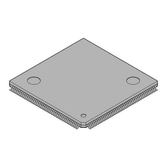
CHAPTER 1 OVERVIEW Pin Layout This section shows the pin layout of the MB91319. ■ Pin Layout of the MB91319 Figure 1.4-1 is a diagram of the pin layout of the MB91319. Figure 1.4-1 Pin Layout of the MB91319 HSYNC1 P02/SCK4/TIN2 HSYNC2 P01/SO4/TIN1... -
Page 32: List Of Pin Functions
CHAPTER 1 OVERVIEW List of Pin Functions This section describes the pin functions of the MB91319. ■ List of Pin Functions Table 1.5-1 lists the pin functions. Table 1.5-1 Pin Functions of the MB91319 (1 / 7) Pin number Pin name I/O circuit type Function HSYNC1... - Page 33 CHAPTER 1 OVERVIEW Table 1.5-1 Pin Functions of the MB91319 (2 / 7) Pin number Pin name I/O circuit type Function VDDIS Data slicer power supply (2.5 V) VSSS Data slicer ground VDDI Internal logic power supply (2.5 V) AVCC A/D power supply AVRH A/D reference power supply...
- Page 34 CHAPTER 1 OVERVIEW Table 1.5-1 Pin Functions of the MB91319 (3 / 7) Pin number Pin name I/O circuit type Function VDDI Internal logic power supply (2.5 V) TRSTX DSU tool reset (this pin is open in the MB91F31x model series.
- Page 35 CHAPTER 1 OVERVIEW Table 1.5-1 Pin Functions of the MB91319 (4 / 7) Pin number Pin name I/O circuit type Function General-purpose port UART 1 serial output General-purpose port SCK1 UART 1 clock I/O General-purpose port PWC input General-purpose port TMI0 Multifunction timer 0 input General-purpose port...
- Page 36 CHAPTER 1 OVERVIEW Table 1.5-1 Pin Functions of the MB91319 (5 / 7) Pin number Pin name I/O circuit type Function General-purpose port SCL3 C clock pin General-purpose port SCL4 C clock pin General-purpose port SDA2 C data pin General-purpose port SDA3 C data pin General-purpose port...
- Page 37 CHAPTER 1 OVERVIEW Table 1.5-1 Pin Functions of the MB91319 (6 / 7) Pin number Pin name I/O circuit type Function General-purpose port General-purpose port UART 4 serial input TIN0 Reload timer 0 trigger input General-purpose port UART 4 serial output TIN1 Reload timer 1 trigger input General-purpose port...
- Page 38 CHAPTER 1 OVERVIEW Table 1.5-1 Pin Functions of the MB91319 (7 / 7) Pin number Pin name I/O circuit type Function General-purpose port General-purpose port General-purpose port General-purpose port VDDI Internal power supply (2.5 V) 48 MHz oscillation pin Ground 48 MHz oscillation pin VDDE 3.3 V power supply...
-
Page 39: Input-Output Circuit Forms
CHAPTER 1 OVERVIEW Input-output Circuit Forms This section describes the input-output circuit types of the MB91319. ■ Input-Output Circuit Types Table 1.6-1 lists the input-output circuit types of the MB91319. Table 1.6-1 Input-Output Circuit Types of the MB91319 (1 / 6) Classification Circuit type Remarks... - Page 40 CHAPTER 1 OVERVIEW Table 1.6-1 Input-Output Circuit Types of the MB91319 (2 / 6) Classification Circuit type Remarks 2.5 V CMOS level output CMOS level hysteresis input with 2.5V standby control Digital output Digital output Digital input Standby control CMOS level output CMOS level hysteresis input with standby control Use of analog input switch...
- Page 41 CHAPTER 1 OVERVIEW Table 1.6-1 Input-Output Circuit Types of the MB91319 (3 / 6) Classification Circuit type Remarks CMOS level hysteresis input without standby control Digital input CMOS level output CMOS level hysteresis input with Pull down control standby control and pull-down resistor Digital output Digital output Digital input...
- Page 42 CHAPTER 1 OVERVIEW Table 1.6-1 Input-Output Circuit Types of the MB91319 (4 / 6) Classification Circuit type Remarks Open-drain output CMOS level hysteresis input with standby control provided Open-drain control Digital output Digital input Standby control Analog pin CMOS level hysteresis input with pull- down resistor Digital input...
- Page 43 CHAPTER 1 OVERVIEW Table 1.6-1 Input-Output Circuit Types of the MB91319 (5 / 6) Classification Circuit type Remarks CMOS level output Digital output Digital output 3 ports for I CMOS level hysteresis input CMOS level output Use of stop control Open-drain control Digital output...
- Page 44 CHAPTER 1 OVERVIEW Table 1.6-1 Input-Output Circuit Types of the MB91319 (6 / 6) Classification Circuit type Remarks CMOS level output CMOS level hysteresis input without standby control Digital output Digital output Digital input CMOS level output CMOS level hysteresis input without standby control Use of pull-down resistor Digital output...
-
Page 45: Chapter 2 Handling The Device
CHAPTER 2 HANDLING THE DEVICE This chapter provides precautions on handling the MB91319 series. Precautions on Handling the Device... -
Page 46: Precautions On Handling The Device
CHAPTER 2 HANDLING THE DEVICE Precautions on Handling the Device This section contains information on preventing a latch up and on the handling of pins. ■ Preventing a Latch Up A latch up can occur if, on a CMOS IC, a voltage higher than VCC or a voltage lower than VSS is applied to an input or output pin or a voltage higher than the rating is applied between VCC and VSS. - Page 47 CHAPTER 2 HANDLING THE DEVICE ■ Power-on Immediately after power-on, be sure to apply a reset with the INIT pin to initialize the settings (INIT). Also immediately after power-on, keep the INIT pin at the L level until the oscillator has reached the required frequency stability.
- Page 48 Therefore, insert damping resistor exteriorly to reduce reflection noise that may affect the internal circuit. ■ Limitations ❍ Common of MB91319 series Clock controller INIT must be kept at the L level until the oscillation stabilization wait time is reached.
- Page 49 In that case, please reset (INIT) from the external INIT pin. Note on using A/D Nevertheless the MB91319 series contains an A/D converter, be sure not to apply the higher power supply than V to the AV About Software Reset of Synchronous Mode To use the software reset of synchronous mode, be sure to meet the following 2 conditions.
- Page 50 CHAPTER 2 HANDLING THE DEVICE ❍ Unique characteristic of the evaluation chip MB91FV319A/R Simultaneous occurrences of software break and user interrupt/NMI (MB91FV319A/R only) If software break and user interrupt/NMI occur together, emulator debugger may: • Stop at a point other than the programmed break points. •...
-
Page 51: Chapter 3 Cpu And Control Units
CHAPTER 3 CPU AND CONTROL UNITS This chapter provides basic information required to understand the functions of the MB91319 series. It covers architecture, specifications, and instructions. Memory Space Internal Architecture Programming Model Data Configuration Word Alignment Memory Map Branch Instructions... -
Page 52: Memory Space
CHAPTER 3 CPU AND CONTROL UNITS Memory Space The MB91319 has a logical address space of 4 GB (2 addresses), which the CPU accesses linearly. ■ Memory Space The MB91319 has a logical address space of 4GB (2 addresses), while the CPU access lineally. -
Page 53: Internal Architecture
CHAPTER 3 CPU AND CONTROL UNITS Internal Architecture The MB91319 CPU is a high-performance core that is designed based on a RISC architecture with high-level function instructions for embedded applications. ■ Features ❍ RISC architecture used Basic instruction: One instruction per cycle ❍... - Page 54 CHAPTER 3 CPU AND CONTROL UNITS ■ Internal Architecture The FR CPU uses the Harvard architecture, in which the instruction bus and data buses are independent of each other. A 32-bit ↔ 16-bit bus converter is connected to the 32-bit bus (F-bus) to provide an interface between the CPU and peripheral resources.
- Page 55 CHAPTER 3 CPU AND CONTROL UNITS ❍ CPU The CPU is a compact implementation of the 32-bit RISC FR architecture. Five instruction pipe lines are used to execute one instruction per cycle. A pipeline consists of the following stages: • Instruction fetch (IF): Outputs an instruction address to fetch an instruction.
- Page 56 CHAPTER 3 CPU AND CONTROL UNITS ■ Overview of Instructions The FR supports the general RISC instruction set as well as logical operation, bit manipulation, and direct addressing instructions optimized for embedded applications. For the instruction set, see "APPENDIX I Instruction Lists". Each instruction is 16-bit long (except for some instructions are 32- or 48-bit long), resulting in superior efficiency of memory use.
- Page 57 CHAPTER 3 CPU AND CONTROL UNITS ❍ Direct addressing Direct addressing instructions are used for access between an I/O and a general-purpose register or between an I/O and the memory. High-speed and high-efficiency access can be achieved since an I/O address is directly specified in an instruction instead of using register indirect addressing.
-
Page 58: Programming Model
CHAPTER 3 CPU AND CONTROL UNITS Programming Model This section explains the programming model in detail. ■ Basic Programming Model Figure 3.3-1 Basic Programming Model 32 bits [Initial value] XXXX XXXX General-purpose register XXXX XXXX 0000 0000 Program counter Program status SCR CCR Table base register Return pointer... - Page 59 CHAPTER 3 CPU AND CONTROL UNITS ■ Registers ❍ General-purpose registers Figure 3.3-2 General-Purpose Registers 32 bits [Initial value] XXXX XXXX XXXX XXXX 0000 0000 Registers R0 to R15 are general-purpose registers. They are used as the accumulator for various operations and pointers for memory access.
- Page 60 CHAPTER 3 CPU AND CONTROL UNITS ❍ Condition code register (CCR) [Initial value] --00XXXX [bit5] Stack flag Specifies the stack pointer to be used as R15. Value Description The system stack pointer (SSP) is used as R15. When an EIT occurs, this bit is automatically set to 0. (Note that the value saved on the stack is the value before it is cleared.) The user stack pointer (USP) is used as R15.
- Page 61 CHAPTER 3 CPU AND CONTROL UNITS [bit1] Overflow flag Indicate whether an overflow has occurred as a result of the operation when the operand is regarded as an integer represented by its 2's complement. Value Description Indicates that the operation did not cause an overflow. Indicates that the operation caused an overflow.
- Page 62 CHAPTER 3 CPU AND CONTROL UNITS ❍ ILM [Initial value] ILM4 ILM3 ILM2 ILM1 ILM0 01111 The interrupt level mask (ILM) register holds an interrupt level mask value. The value held in ILM is used as a level mask. An interrupt request to the CPU is accepted only when its interrupt level is higher than the level indicated in this ILM.
- Page 63 CHAPTER 3 CPU AND CONTROL UNITS ❍ Return pointer (RP) 0 [Initial value] XXXXXXXX The return pointer holds the address returned from a subroutine. When a CALL instruction is executed, the PC value is transferred to this RP. When a RET instruction is executed, the RP contents are transferred to PC. The initial value after reset is undefined.
- Page 64 CHAPTER 3 CPU AND CONTROL UNITS ❍ Multiply and divide register The multiply and divide registers are 32-bit long. The initial value after reset is undefined. When multiplication is executed For a 32-bit-by-32-bit multiplication, the 64-bit long operation result is stored in the multiply and divide registers as follows: MDH: High-order 32 bits MDL: Low-order 32 bits...
-
Page 65: Data Configuration
CHAPTER 3 CPU AND CONTROL UNITS Data Configuration The MB91319 uses the following two data ordering methods: • Bit ordering • Byte ordering • Bit ordering ■ Bit Ordering Use the little endian method for bit ordering. bit 31 30 29 28 27 26 25 24 23 22 21 20 19 18 17 16 15 14 13 12 11 10 9 8 7 6 5 4 3 2 1 0 ■... -
Page 66: Word Alignment
CHAPTER 3 CPU AND CONTROL UNITS Word Alignment Since instructions and data are accessed in byte units, the addresses at which they are placed depend on the instruction length or the data width. ■ Program Access A program must be placed at an address that is a multiple of 2. Bit0 of the PC is set to 0 if the PC is updated when an instruction is executed. -
Page 67: Memory Map
CHAPTER 3 CPU AND CONTROL UNITS Memory Map This section shows the memory map for the MB91319. ■ Memory Map The address space is 32 bits linear. Figure 3.6-1 Memory Map 0000 0000 Byte data 0000 0100 Halfword data Direct addressing area 0000 0200 Word data 0000 0400... -
Page 68: Branch Instructions
CHAPTER 3 CPU AND CONTROL UNITS Branch Instructions An operation with or without a delay slot can be specified for a branch instruction used in the MB91319. ■ Branch Instruction with Delay Slot Instructions written as follows perform a branch operation with a delay slot: JMP:D CALL:D label12... - Page 69 CHAPTER 3 CPU AND CONTROL UNITS [Example] LDI:32 #Label, JMP:D Branch to Label LDI:8 No effect on the branch destination address RP referenced by the RET:D instruction is not affected even though RP is updated by the instruction in the delay slot. [Example] RET:D Branch to address defined beforehand in RP...
- Page 70 CHAPTER 3 CPU AND CONTROL UNITS ❍ Step trace trap A step trace trap does not occur between the execution of a branch instruction with a delay slot and the delay slot. ❍ Interrupt NMI An interrupt NMI is not accepted between the execution of a branch instruction with a delay slot and the delay slot.
-
Page 71: Eit (Exception, Interrupt, And Trap)
CHAPTER 3 CPU AND CONTROL UNITS EIT (Exception, Interrupt, and Trap) EIT, a generic term for exception, interrupt, and trap, refers to suspending program execution if an event occurs during execution and then executing another program. ■ EIT (Exception, Interrupt, and Trap) An exception is an event that occurs related to the execution context. -
Page 72: Eit Interrupt Levels
CHAPTER 3 CPU AND CONTROL UNITS 3.8.1 EIT Interrupt Levels The interrupt levels are 0 to 31 and are managed with five bits. ■ Interrupt Levels Table 3.8-1 shows the allocation of the levels. Table 3.8-1 EIT Interrupt Levels Level Binary Decimal 00000... - Page 73 CHAPTER 3 CPU AND CONTROL UNITS ■ Interrupt Level Mask (ILM) Register A PS register (bit20 to bit16) that holds an interrupt level mask value. The CPU accepts only an interrupt request sent to it with an interrupt level higher than the level indicated by the ILM.
-
Page 74: Interrupt Control Unit (Icr)
CHAPTER 3 CPU AND CONTROL UNITS 3.8.2 Interrupt Control Unit (ICR) The interrupt control register (ICR: Interrupt Control Register), located in the interrupt controller, sets the level of an interrupt request. An ICR is provided for each of the interrupt request inputs. The ICR is mapped on the I/O space and is accessed from the CPU through a bus. -
Page 75: System Stack Pointer (Ssp)
CHAPTER 3 CPU AND CONTROL UNITS 3.8.3 System Stack Pointer (SSP) The system stack pointer (SSP) is used to point to the stack to save and restore data when EIT is accepted or a return operation occurs. ■ System Stack Pointer (SSP) bit 31 [Initial value] 00000000... -
Page 76: Table Base Register (Tbr)
CHAPTER 3 CPU AND CONTROL UNITS 3.8.4 Table Base Register (TBR) Indicate the beginning address of the vector table for EIT. ■ Table Base Register (TBR) The table base register (TBR) consists of 32 bits as shown below: bit 31 [Initial value] 000FFC00 Obtain a vector address by adding to the TBR the offset value predetermined for an EIT cause. - Page 77 CHAPTER 3 CPU AND CONTROL UNITS Table 3.8-3 Vector Table (1 / 3) Interrupt number Default Interrupt source Interrupt level Offset address of Decimal Hexadecimal Reset 000FFFFC Mode vector 000FFFF8 Reserved for system 000FFFF4 Reserved for system 000FFFF0 Reserved for system 000FFFEC Reserved for system 000FFFE8...
- Page 78 CHAPTER 3 CPU AND CONTROL UNITS Table 3.8-3 Vector Table (2 / 3) Interrupt number Default Interrupt source Interrupt level Offset address of Decimal Hexadecimal Maskable interrupt source ICR13 000FFF88 Maskable interrupt source ICR14 000FFF84 Maskable interrupt source ICR15 000FFF80 Maskable interrupt source ICR16 000FFF7C...
- Page 79 CHAPTER 3 CPU AND CONTROL UNITS Table 3.8-3 Vector Table (3 / 3) Interrupt number Default Interrupt source Interrupt level Offset address of Decimal Hexadecimal Maskable interrupt source ICR43 000FFF10 Maskable interrupt source ICR44 000FFF0C Maskable interrupt source ICR45 000FFF08 Maskable interrupt source ICR46 000FFF04...
-
Page 80: Multiple Eit Processing
CHAPTER 3 CPU AND CONTROL UNITS 3.8.5 Multiple EIT Processing If multiple EIT causes occur at the same time, the CPU repeats the operation of selecting and accepting one of the EIT causes, executing the EIT sequence, and then detecting EIT causes again. If there are no more EIT causes be accepted while the CPU is detecting EIT causes, the CPU executes the handler instruction of the last accepted EIT cause. - Page 81 CHAPTER 3 CPU AND CONTROL UNITS In consideration of masking other causes after an EIT cause is accepted, the handlers of EIT causes that occur at the same time are executed in the order shown in Table 3.8-5. Table 3.8-5 Order of Executing EIT Handlers Order of executing Cause handlers...
-
Page 82: Eit Operations
CHAPTER 3 CPU AND CONTROL UNITS 3.8.6 EIT Operations This section describes EIT operations. ■ EIT Operations In the following, it is assumed that the destination source PC indicates the address of the instruction that detected an EIT cause. In addition, "address of the next instruction" means that the instruction that detected EIT is as follows: •... - Page 83 CHAPTER 3 CPU AND CONTROL UNITS If a user interrupt or NMI request is accepted when EIT requests are detected, the CPU operates as follows, using an interrupt number corresponding to the accepted interrupt request. Parentheses show an address indicated by the register. ■...
- Page 84 CHAPTER 3 CPU AND CONTROL UNITS ■ Operation of Step Trace Trap Set the T flag in the SCR of the PS to enable the step trace function. A trap and a break then occur every time an instruction is executed. [Step trace trap detection conditions] T flag =1 There is no delayed branch instruction.
- Page 85 CHAPTER 3 CPU AND CONTROL UNITS ■ No-coprocessor Trap If a coprocessor instruction using a coprocessor that is not installed is executed, a no- coprocessor trap occurs. [Operation] 1. SSP-4 → SSP 2. PS → (SSP) 3. SSP-4 → SSP 4.
-
Page 86: Operating Modes
CHAPTER 3 CPU AND CONTROL UNITS Operating Modes Two operating modes are provided: bus mode and access mode. This section describes these modes. ■ Operating Modes Bus mode Access mode Single chip 16-bit bus width Internal ROM/external bus External ROM/external bus 8-bit bus width ❍... - Page 87 CHAPTER 3 CPU AND CONTROL UNITS ■ Mode Settings For the MB91319, set the operating mode using the mode pins (MD3, MD2, MD1, and MD0) and the mode register (MODR). ❍ Mode pins Use the three mode pins (MD3, MD2, MD1, and MD0) to specify mode vector fetch. Mode pin Reset vector Mode name...
- Page 88 CHAPTER 3 CPU AND CONTROL UNITS Note: Be sure to set bit7 to bit3 to 00000. If any other value is set for these bits, operation is unpredictable. [bit2] Reserved bit Be sure to set this bit to 1. [bit1, bit0] WTH1, WTH0 (Bus width specification bit) These bits indicate the bus width specification to be used in external bus mode.
-
Page 89: Reset (Device Initialization)
CHAPTER 3 CPU AND CONTROL UNITS 3.10 Reset (Device Initialization) This section describes a reset (that is, initialization) of the MB91319. ■ Reset (Device Initialization) If a reset source occurs, the device stops all the programs and hardware operations and completely initializes the state. -
Page 90: Reset Levels
CHAPTER 3 CPU AND CONTROL UNITS 3.10.1 Reset Levels The reset operations of the MB91319 are classified into two levels, each of which has different causes and initialization operations. This section describes these reset levels. ■ Settings Initialization Reset (INIT) The highest-level reset, which initializes all settings, is called a settings initialization reset (INIT). -
Page 91: Reset Sources
CHAPTER 3 CPU AND CONTROL UNITS 3.10.2 Reset Sources This section describes the reset sources and the reset levels in the MB91319. To determine reset sources that have occurred in the past, read the RSRR (reset source register). For more information about registers and flags described in this section, see "3.11.5 Block Diagram of Clock Generation Controller"... - Page 92 CHAPTER 3 CPU AND CONTROL UNITS Reference: For details on using software reset of synchronous mode, see restrictions of bit7: SYNCR bit of TBCR (time base counter control register). ■ Watchdog Reset Writing to the watchdog timer control register (RSRR) starts the watchdog timer. Unless A5 is written to the time base counter clear register (CTBR) within the cycle specified in bit9 and bit8 (WT1 and WT0 bits) in the RSRR, a watchdog reset request occurs.
-
Page 93: Reset Sequence
CHAPTER 3 CPU AND CONTROL UNITS 3.10.3 Reset Sequence When a reset source no longer exists, the device starts to execute the reset sequence. A reset sequence has different operations depending on the reset level. This section describes the operations of the reset sequence for different reset levels. ■... -
Page 94: Oscillation Stabilization Wait Time
CHAPTER 3 CPU AND CONTROL UNITS 3.10.4 Oscillation Stabilization Wait Time If a device returns from the state in which the original oscillation was or may have been stopped, the device automatically enters the oscillation stabilization wait state. This function prevents the use of oscillator output after starting before oscillation has stabilized. - Page 95 CHAPTER 3 CPU AND CONTROL UNITS ■ Selecting an Oscillation Stabilization Wait Time The oscillation stabilization wait time is measured with the built-in time base counter. If a source for an oscillation stabilization wait occurs and the device enters the oscillation stabilization wait state, the built-in time base counter is initialized and then it starts to measure the oscillation stabilization wait time.
-
Page 96: Reset Operation Modes
CHAPTER 3 CPU AND CONTROL UNITS 3.10.5 Reset Operation Modes Two modes for an operation initialization reset (RST) are provided: normal (asynchronous) reset mode and synchronous reset mode. The operation initialization reset mode is selected with bit7 (SYNCR bit) of the time base counter control register (TBCR). -
Page 97: Clock Generation Control
CHAPTER 3 CPU AND CONTROL UNITS 3.11 Clock Generation Control This section describes clock generation and control. ■ Clock Generation Control The internal operating clock of the MB91319 is generated as follows: • Selection of a source clock: Select a clock supply source. •... -
Page 98: Pll Controls
CHAPTER 3 CPU AND CONTROL UNITS 3.11.1 PLL Controls The operation (oscillation) enable and disable and multiply-by-rate setting can be independently controlled for each of the PLL oscillator circuits provided for each of main source clock and subclock. Each control is set in the clock source control register (CLKR). - Page 99 CHAPTER 3 CPU AND CONTROL UNITS ■ PLL Multiply-by Rate Set the multiply-by rate of the main PLL in bit14 to bit12 (PLL1S2, PLL1S1, and PLL1S0 bits) of the clock source control register (CLKR). After a setting initialization reset (INIT), all bits are initialized to 0. ❍...
-
Page 100: Oscillation Stabilization Wait Time And Pll Lock Wait Time
CHAPTER 3 CPU AND CONTROL UNITS 3.11.2 Oscillation Stabilization Wait Time and PLL Lock Wait Time If a clock selected as the source clock is not already stabilized, an oscillation stabilization wait time is required (See "3.10.4 Oscillation Stabilization Wait Time"). For a PLL, a lock wait time is required after operation starts until the output stabilizes to the specified frequency. - Page 101 CHAPTER 3 CPU AND CONTROL UNITS ■ Wait Time after Returning from Stop Mode If, after a program starts execution, the device enters stop mode and then stop mode is cleared, the oscillation stabilization wait time specified in the program is internally generated. If the clock oscillation circuit selected as the source clock is set to stop in stop mode, the oscillation stabilization wait time of the oscillation circuit or the lock wait time of the PLL in use, whichever is longer, is required.
-
Page 102: Clock Distribution
CHAPTER 3 CPU AND CONTROL UNITS 3.11.3 Clock Distribution An operating clock for each function is generated based on the base clock generated from the source clock. A total of three internal operating clocks are provided. A divide- by rate can be set independently for each of them. This section describes these internal operating clocks. - Page 103 CHAPTER 3 CPU AND CONTROL UNITS ■ Peripheral Clock (CLKP) This clock is used for peripheral circuits and peripheral buses. It is used by the following circuits: • Peripheral bus • Clock controller (only for the bus interface) • Interrupt controller •...
-
Page 104: Clock Division
CHAPTER 3 CPU AND CONTROL UNITS 3.11.4 Clock Division A divide-by rate can be set independently for each of the internal operating clocks. With this function, an optimal operating frequency can be set for each circuit. ■ Clock Division Set a divide-by rate in Basic Clock Division Setting Register 0 (DIVR0) and Basic Clock Division Setting Register 1 (DIVR1). -
Page 105: Block Diagram Of Clock Generation Controller
CHAPTER 3 CPU AND CONTROL UNITS 3.11.5 Block Diagram of Clock Generation Controller This section provides a block diagram of the clock generation controller. The detailed description of register in the figure refers to 8 Detailed explanation for register of clock generation controller. ■... -
Page 106: Register Of Clock Generation Controller
CHAPTER 3 CPU AND CONTROL UNITS 3.11.6 Register of Clock Generation Controller This section describes the functions of registers to be used in the clock generation controller. ■ Reset Source Register/Watchdog Timer Control Register (RSRR) Figure 3.11-2 shows the configuration of the reset source register/watchdog timer control register (RSRR). - Page 107 CHAPTER 3 CPU AND CONTROL UNITS [bit12] (Reserved bit) This bit is reserved. [bit11] SRST (Software ReSeT occurred) This bit indicates whether a reset (RST) occurred due to writing to the SRST bit of the STCR register (a software reset). No RST occurred due to a software reset.
- Page 108 CHAPTER 3 CPU AND CONTROL UNITS ■ Standby Control Register (STCR) Figure 3.11-3 shows the configuration of the standby control register (STCR). Figure 3.11-3 Configuration of Standby Control Register (STCR) Bits Address:00000481 STOP SLEEP HIZ SRST OS1 OS0 OSCD2 OSCD1 Initial value (INIT pin) Initial value (HSTX) Initial value (INIT)
- Page 109 CHAPTER 3 CPU AND CONTROL UNITS [bit5] HIZ (HIZ mode) This bit controls the pin state in stop mode. The pin state before stop mode entered is maintained. Pin output is set to high-impedance state in stop mode (initial value). •...
- Page 110 CHAPTER 3 CPU AND CONTROL UNITS [bit1] OSCD2 (OSCillation Disable mode for XIN2) This bit controls stopping of the sub-oscillation input (XIN2) in stop mode. Not stopping the sub-oscillation in stop mode Stopping the sub-oscillation in stop mode (initial value) •...
- Page 111 CHAPTER 3 CPU AND CONTROL UNITS [bit14] TBIE (TimeBasetimer Interrupt Enable) This bit is the time base timer interrupt request output enable bit. It controls output of an interrupt request when the interval time of the time base counter has elapsed.
- Page 112 CHAPTER 3 CPU AND CONTROL UNITS [bit9] SYNCR (SYNChronous Reset enable) This bit is the synchronous reset enable bit. This bit specifies whether normal reset operation or synchronous reset operation is executed when an operation initialization reset (RST) request occurs. Normal reset operation performs a reset (RST) immediately.
- Page 113 CHAPTER 3 CPU AND CONTROL UNITS ■ Time Base Counter Clear Register (CTBR) Figure 3.11-5 shows the configuration of the time base counter clear register (CTBR) bits. Figure 3.11-5 Configuration of Time Base Counter Clear Register (CTBR) Bits Address: 00000483 Initial value (INIT) Initial value (RST) The time base counter clear register initializes the time base counter.
- Page 114 CHAPTER 3 CPU AND CONTROL UNITS ■ Clock Source Control Register (CLKR) Figure 3.11-6 shows the configuration of the clock source control register (CLKR) bits. Figure 3.11-6 Configuration of Clock Source Control Register (CLKR) Bits Address: 00000484 PLL2S0 PLL1S2 PLL1S1 PLL1S0 PLL2EN PLL1EN CLKS1 CLKS0 R/W R/W R/W R/W R/W R/W R/W R/W Initial value (INIT) Initial value (RST)
- Page 115 CHAPTER 3 CPU AND CONTROL UNITS Table 3.11-2 Main PLL Multiply-By Rate Settings Main PLL multiply- PLL1S2 PLL1S1 PLL1S0 If the source oscillation is 16.5 MHz by rate × 1 (equal) For source oscillator 10 (MHz), φ = 100[ns] (10 (MHz)) ×...
- Page 116 CHAPTER 3 CPU AND CONTROL UNITS [bit9, bit8] CLKS1, CLKS0 (CLocK source Select) These bits set the clock source that will be used by the FRex core. The values written to these bits determine the clock source, which can be selected from the three types shown in Table 3.11-3.
- Page 117 CHAPTER 3 CPU AND CONTROL UNITS ■ Base Clock Division Setting Register 0 (DIVR0) Figure 3.11-7 shows the configuration of the Base Clock Division Setting Register 0 (DIVR0) bits. Figure 3.11-7 Configuration of Base Clock Division Setting Register 0 (DIVR0) Bits Address: 00000486 R/W R/W Initial value (INIT)
- Page 118 CHAPTER 3 CPU AND CONTROL UNITS [bit11 to bit8] P3, P2, P1, P0 (clkP divide select 3-0) These bits are the clock divide-by rate setting bits of the peripheral clock (CLKP). Set the clock divide-by rate of the peripheral circuit and the peripheral bus clock (CLKP). The values written to these bits determine the divide-by rate (clock frequency) of the peripheral circuit and the peripheral bus clock in relation to the base clock, which can be selected from the 16 types shown in Table 3.11-6.
- Page 119 CHAPTER 3 CPU AND CONTROL UNITS If the setting in this register is changed, the new divide-by rate takes effect for the clock rate following the one during which the setting was made. [bit7 to bit4] T3, T2, T1, T0 (clkT divide select 3-0) These bits are the clock divide-by rate setting bits of the external bus clock (CLKT).
- Page 120 CHAPTER 3 CPU AND CONTROL UNITS Table 3.11-7 Clock Divide-By Rate (External Bus Clock) Settings Clock frequency: if the source oscillation is Clock divide-by rate 10 [MHz] and the PLL is multiplied by 4 φ 40 [MHz] (initial value) φ × 2 (divided by 2) 20 [MHz] φ...
- Page 121 CHAPTER 3 CPU AND CONTROL UNITS If INIT switches the clock source to the main clock when this bit stops main clock oscillation, the main oscillation stabilization wait time is also required. If the settings of bit3 and bit2 (OS1 and OS0) of the standby control register (STCR) do not satisfy the main oscillation stabilization wait time, the operation after return is unpredictable.
-
Page 122: Peripheral Circuits Of Clock Controller
CHAPTER 3 CPU AND CONTROL UNITS 3.11.7 Peripheral Circuits of Clock Controller This section describes the peripheral circuit functions of the clock controller. ■ Time Base Counter The clock controller has a 26-bit time base counter that runs on the system base clock. The time base counter is used to measure the oscillation stabilization wait time in addition to having the uses listed below (For more information about the oscillation stabilization wait time, see "3.10.4 Oscillation Stabilization Wait Time"). - Page 123 CHAPTER 3 CPU AND CONTROL UNITS [Suspending the watchdog timer (automatic postponement)] If program operation stops on the CPU, the watchdog reset generation flag is initialized and generation of a watchdog reset is postponed. Stopping of program operation specifically refers to the following statuses: •...
- Page 124 CHAPTER 3 CPU AND CONTROL UNITS [Clearing of the time base counter due to the device state] All bits of the time base counter are cleared to 0 at the same time if the device enters one of the following states: •...
- Page 125 CHAPTER 3 CPU AND CONTROL UNITS ■ Main Clock Oscillation Stabilization Wait Timer (for the Subclock Select) The main clock oscillation stabilization wait timer is a 26-bit free-run timer that performs incremental counting in synchronization with the main clock. The operation of this timer is not affected by the clock source selection or the clock divide-by rate.
-
Page 126: Device State Control
CHAPTER 3 CPU AND CONTROL UNITS 3.12 Device State Control This section describes the states of the MB91319 and their control. ■ Device State Control 3.12.1 Device States and State Transitions 3.12.2 Low-power Modes... -
Page 127: Device States And State Transitions
CHAPTER 3 CPU AND CONTROL UNITS 3.12.1 Device States and State Transitions This section describes device operating states and the transition between operating states. ■ Transition of Device States Figure 3.12-1 shows the transition of device states. - Page 128 CHAPTER 3 CPU AND CONTROL UNITS Figure 3.12-1 Transition of Device States Priority of state transition requests INTX pin = 0 (INIT) Settings initialization reset INTX pin = 1 (clearance of INIT state) (INIT) request End of oscillation stabilization wait time End of oscillation stabilization Release from reset (RST) state wait time...
- Page 129 CHAPTER 3 CPU AND CONTROL UNITS ■ RUN State (Normal Operation) In the RUN state, a program is being executed. All internal clocks are supplied and all circuits are enabled. For the 16-bit peripheral bus, however, only the bus clock is stopped, when it is not being accessed.
- Page 130 CHAPTER 3 CPU AND CONTROL UNITS ■ Oscillation Stabilization Wait RUN State In the oscillation stabilization wait RUN state, the device is stopped. This state occurs after a return from the stop state. All internal circuits except the clock generation controller (time base counter and device state controller) are stopped.
- Page 131 CHAPTER 3 CPU AND CONTROL UNITS ■ Settings Initialization Reset (INIT) State In the settings initialization reset (INIT) state, all settings are initialized. This state occurs if a settings initialization reset (INIT) is accepted or the hardware standby state is ended. Execution of a program on the CPU is stopped and the program counter is initialized.
-
Page 132: Low-Power Modes
CHAPTER 3 CPU AND CONTROL UNITS 3.12.2 Low-power Modes This section describes the low-power modes, some MB91319 states, and how to use the low-power modes. ■ Low-power Modes The MB91319 has the following two low-power modes: • Sleep mode: The device enters the sleep state due to writing to a register. •... - Page 133 CHAPTER 3 CPU AND CONTROL UNITS [Sources of return from the sleep state] • Generation of a valid interrupt request If an interrupt request with an interrupt level other than interrupt disabled (1F ) occurs, sleep mode is cleared and the RUN state (normal operation state) is entered. To prevent sleep mode from being cleared even when an interrupt request occurs, set interrupt disabled (1F ) as the interrupt level in the corresponding ICR.
- Page 134 CHAPTER 3 CPU AND CONTROL UNITS [Circuits that do not stop in the stop state] • Oscillation circuits that are set not to stop • If 0 is set for bit1 (OSCD2 bit) of the standby control register (STCR), the subclock oscillation circuit in the stop state is not stopped.
- Page 135 CHAPTER 3 CPU AND CONTROL UNITS [Normal and synchronous standby operations] If 1 is set for bit8 (SYNCS bit) of the time base counter control register (TBCR), synchronous standby operation is enabled. In this case, simply writing to the STOP bit does not cause a transition to the stop state.
-
Page 136: Watch Timer
CHAPTER 3 CPU AND CONTROL UNITS 3.13 Watch Timer The watch timer is a 15-bit free-run timer that performs incremental counting in synchronization with the subclock. The watch timer has an interval timer function to generate interrupts repeatedly at fixed time intervals. The internal time can be selected from four types as follow. - Page 137 CHAPTER 3 CPU AND CONTROL UNITS ■ Block Diagram Figure 3.13-1 shows the block diagram of the watch timer. Figure 3.13-1 Block Diagram of the Watch Timer Watch timer counter (31.25ms) (0.25s) Interval timer (0.50s) selector (1.00s) Reset (INIT) Counter clear circuit Watch timer interrupt Watch timer control...
- Page 138 CHAPTER 3 CPU AND CONTROL UNITS ■ Watch Timer Control Register Figure 3.13-2 shows the bit configuration of the watch timer control register. Figure 3.13-2 Bit Configuration of Watch Timer Control Register Initial value WPCR At INIT At RST Access 0000 048C [bit15] WIF (watch timer interrupt flag) This bit is the watch timer interrupt flag.
- Page 139 CHAPTER 3 CPU AND CONTROL UNITS [bit10, bit9] WS1, WS0 (watch timer interval select 1, 0) These bits select the interval of the interval timer. One of the following four intervals is selected according to the output bits of the watch timer counter: Interval timer interval (at FCL = 32.768 kHz) (31.25 ms) (default value)
- Page 140 CHAPTER 3 CPU AND CONTROL UNITS ■ Operation of Interval Timer Function The watch timer counter continues incremental counting while the subclock is running. When subclock oscillation stops, counting stops in the following cases: • Counting stops when bit11 (PLL2EN) of the clock source register (CLKR) is 0. On the MB31319, the PLL2EN is cleared to 0 at reset by an INIT request.
- Page 141 CHAPTER 3 CPU AND CONTROL UNITS ■ Operation of The Watch Timer Figure 3.13-3 shows the counter states at start of watch timer, switching to the subclock, and transition to stop mode during operation with the subclock. Figure 3.13-3 Counter States at Transition to Stop Mode 7FFF Value of counter 4000...
-
Page 142: Main Clock Oscillation Stabilization Wait Timer
CHAPTER 3 CPU AND CONTROL UNITS 3.14 Main Clock Oscillation Stabilization Wait Timer The main clock oscillation stabilization wait timer is a 23-bit free-run timer that performs incremental counting in synchronization with the main clock. The main clock oscillation stabilization wait timer has an interval timer function to generate interrupts repeatedly at fixed time intervals. - Page 143 CHAPTER 3 CPU AND CONTROL UNITS ■ Block Diagram Figure 3.14-1 Block Diagram of the Main Clock Oscillation Stabilization Wait Timer Main clock oscillation stabilization wait timer counter (410µs) Interval timer selector (13.1ms) (839ms) Reset Counter Main clock oscillation (INIT) clear circuit stabilization wait timer interrupt request...
- Page 144 CHAPTER 3 CPU AND CONTROL UNITS ■ Main Clock Oscillation Stabilization Wait Timer Control Register Figure 3.14-2 shows the bit configuration of the main clock oscillation stabilization wait timer control register. Figure 3.14-2 Bit Configuration of Main Clock Oscillation Stabilization Wait Timer Control Register Initial value OSCR At INIT...
- Page 145 CHAPTER 3 CPU AND CONTROL UNITS [bit10, bit9] WS1, WS0 (watch timer interval select 1, 0) These bits select the interval of the interval timer. One of the following three intervals is selected according to the output bits of the main clock oscillation stabilization wait timer counter: Interval timer interval (at F = 10 MHz)
- Page 146 CHAPTER 3 CPU AND CONTROL UNITS ■ Operation of Interval Timer Function The main clock oscillation stabilization wait timer counter continues incremental counting while the main clock is oscillated. When main clock oscillation stops, counting stops in the following case: •...
- Page 147 CHAPTER 3 CPU AND CONTROL UNITS ■ Operation of the Main Clock Oscillation Stabilization Wait Timer Figure 3.14-3 shows the counter states at the start of the main clock oscillation stabilization wait time and switching to the main clock. Figure 3.14-3 Counter States at Switching to the Main Clock 7 FFFFF Value of counter Main clock oscillation...
- Page 148 CHAPTER 3 CPU AND CONTROL UNITS...
-
Page 149: Chapter 4 I/O Port
CHAPTER 4 I/O PORT This chapter describes the I/O ports and the configuration and functions of registers. Overview of the I/O Port I/O Port Registers... -
Page 150: Overview Of The I/O Port
CHAPTER 4 I/O PORT Overview of the I/O Port This section provides an overview of the I/O port. ■ Basic Block Diagram of the I/O Port The pins of this LSI device can be used as I/O ports if settings are made so that the corresponding pins are not used for the inputs and outputs of the peripheral circuits. - Page 151 CHAPTER 4 I/O PORT ■ I/O Port Modes The I/O port has the following four modes: ❍ Port input mode (PFR=0 & DDR=0) • PDR read: Reads the level of the corresponding external pin. • PDR write: Writes a setting value to the PDR. ❍...
-
Page 152: I/O Port Registers
CHAPTER 4 I/O PORT I/O Port Registers This section describes the configuration and functions of the I/O port registers. ■ Configuration of the Port Data Registers (PDR) Figure 4.2-1 shows the configuration of the port data registers (PDRs). Figure 4.2-1 Configuration of the Port Data Registers (PDR) PDR0 Initial value Access Address: 00000010... - Page 153 CHAPTER 4 I/O PORT ■ Configuration of the Data Direction Registers (DDR) Figure 4.2-2 shows the configuration of the data direction registers (DDRs). Figure 4.2-2 Configuration of the Data Direction Registers (DDR) DDR0 Initial value Access Address: 00000400 00000000 DDR1 Initial value Access Address: 00000401 00000000...
- Page 154 CHAPTER 4 I/O PORT ■ Configuration of the Port Function Registers (PFR) Figure 4.2-3 shows the configuration of the port function registers (PFRs). Figure 4.2-3 Configuration of the Data Direction Registers (PFR) PFR0 Initial value Access Address: 00000410 2CE4 2CE3 2CE2 2CE1 2CE0...
- Page 155 CHAPTER 4 I/O PORT ■ Initial Values and Functions of the Port Function Registers (PFRs) Table 4.2-1 lists the initial values and functions of the port function registers (PFRs). Table 4.2-1 Initial Values and Functions of the Port Function Registers (PFRs) (1 / 4) Register name Bit name Bit value...
- Page 156 CHAPTER 4 I/O PORT Table 4.2-1 Initial Values and Functions of the Port Function Registers (PFRs) (2 / 4) Register name Bit name Bit value Function PFR1 General-purpose port UART3 S03 output General-purpose port SCKE3 SCK3 output UART2 General-purpose port S02 output SCKE2 General-purpose port...
- Page 157 CHAPTER 4 I/O PORT Table 4.2-1 Initial Values and Functions of the Port Function Registers (PFRs) (3 / 4) Register name Bit name Bit value Function PFR3 TME3 General-purpose port TMO2 output TME2 General-purpose port TMO2 output TME1 General-purpose port TMO1 output TME0 General-purpose port...
- Page 158 CHAPTER 4 I/O PORT Table 4.2-1 Initial Values and Functions of the Port Function Registers (PFRs) (4 / 4) Register name Bit name Bit value Function PFR5 ADE7 Function as general-purpose port. Function as AN7 input. ADE6 Function as general-purpose port. Function as AN6 input.
-
Page 159: 16-Bit Reload Timer
CHAPTER 5 16-BIT RELOAD TIMER This chapter describes the 16-bit reload timer, the configuration and functions of registers, and 16-bit reload timer operation. 5.1 Overview of the 16-bit Reload Timer 5.2 16-bit Reload Timer Registers 5.3 16-bit Reload Timer Operation... -
Page 160: Overview Of The 16-Bit Reload Timer
■ Overview of the 16-bit Reload Timer The MB91319 series has three built-in channels, numbered 0 to 2, for the 16-bit reload timer. Channels 0 and 1 support the activation of DMA transfers resulting from interrupts. -
Page 161: 16-Bit Reload Timer Registers
CHAPTER 5 16-BIT RELOAD TIMER 16-bit Reload Timer Registers This section describes the configuration and functions of the registers used by the 16-bit reload timer. ■ 16-bit Reload Timer Registers Figure 5.2-1 16-bit Reload Timer Registers CSL1 CSL0 MOD2 MOD1 Control status register (TMCSR) MOD0... -
Page 162: Control Status Register (Tmcsr)
CHAPTER 5 16-BIT RELOAD TIMER 5.2.1 Control Status Register (TMCSR) The control status register (TMCSR) controls the operating modes and interrupts of the 16-bit timer. ■ Bit Configuration of the Control Status Register (TMCSR) Figure 5.2-2 Bit Configuration of the Control Status Register (TMCSR) TMCSR Address: Initial value... - Page 163 CHAPTER 5 16-BIT RELOAD TIMER [bit9, bit8, bit7] MOD2, MOD1, MOD0 (MODe) These bits set the operating modes and the functions of the input-output pins. The MOD2 bit selects the function of an input pin. If it is set to "0", the input pin becomes the trigger input pin.
- Page 164 CHAPTER 5 16-BIT RELOAD TIMER [bit5] OUTL This bit sets the output level of the TOUT pin. The pin levels are reversed while this bit is set to "0" and "1". Specify an output waveform using a combination of this bit, bit4 (RELD bit), and the corresponding bit of the PFR register of the I/O port.
-
Page 165: 16-Bit Timer Register (Tmr)
CHAPTER 5 16-BIT RELOAD TIMER 5.2.2 16-bit Timer Register (TMR) The 16-bit timer register (TMR) is a register to which the count value of the 16-bit timer can be read. The initial value is undefined. Be sure to read this register using a 16-bit data transfer instruction. ■... -
Page 166: 16-Bit Reload Register (Tmrlr)
CHAPTER 5 16-BIT RELOAD TIMER 5.2.3 16-bit Reload Register (TMRLR) The 16-bit reload register (TMRLR) holds the initial value of a counter. The initial value is undefined. Be sure to read this register using a 16-bit data transfer instruction. ■ Bit Configuration of the 16-bit Reload Register (TMRLR) Figure 5.2-4 shows the bit configuration of the 16-bit reload register (TMRLR). -
Page 167: 16-Bit Reload Timer Operation
CHAPTER 5 16-BIT RELOAD TIMER 16-bit Reload Timer Operation This section describes the following operations of the 16-bit reload timer: • Internal clock operation • Underflow operation • Operation of the input pin function • Operation of the output pin function ■... - Page 168 CHAPTER 5 16-BIT RELOAD TIMER ■ Underflow Operation An underflow is an event in which the counter value changes from 0000 to FFFF . Thus, an underflow occurs at the count of [Reload register setting value + 1]. If the RELD bit of the control status register (TMCSR) is set to "1" when an underflow occurs, the contents of the 16-bit reload register (TMRLR) are loaded and the count operation is continued.
- Page 169 CHAPTER 5 16-BIT RELOAD TIMER ■ Operation of the Input Pin Function (in Internal Clock Mode) If the internal clock is selected as the clock source, the TIN pin can be used as the trigger or gate input. ● Trigger input operation If the TIN pin is used as the trigger input, the input of a valid edge loads the contents of the 16-bit reload register (TMRLR) into the counter, clears the internal prescaler, and then starts the count operation.
- Page 170 CHAPTER 5 16-BIT RELOAD TIMER ■ External Event Count Operation If the external clock is selected, the TIN pin becomes the external event input pin and valid edges defined in the register are counted. The pulse width of the TIN pin must be 2T (where T is a peripheral clock machine cycle) or more.
- Page 171 CHAPTER 5 16-BIT RELOAD TIMER ■ Other Operation Channels 0 and 1 of the 16-bit reload timer support the start of DMA transfer occurring due to interrupt request signals. The DMA controller clears the interrupt flag of the reload timer as soon as a transfer request is accepted.
- Page 172 CHAPTER 5 16-BIT RELOAD TIMER ■ Precautions on Using the 16-bit Reload Timer ● Internal prescaler The internal prescaler is enabled if a trigger (software or external trigger) is applied while bit1 (timer enable: CNTE) of the control status register (TMCSR) is set to "1". Even when only gate count mode is to be used, be sure to apply a trigger one time before a valid gate level is input.
-
Page 173: Chapter 6 Programmable Pulse Generator (Ppg) Timer
CHAPTER 6 PROGRAMMABLE PULSE GENERATOR (PPG) TIMER This chapter gives an outline of the PPG (Programmable Pulse Generator) timer and explains the register configuration and functions and the timer operations. Outline Block Diagram of the PPG Timer Registers of the PPG Timer PWM Mode One-shot Mode Interrupts... -
Page 174: Outline
CHAPTER 6 PROGRAMMABLE PULSE GENERATOR (PPG) TIMER Outline The PPG timer can efficiently output highly accurate PWM waveforms. The MB91319 has four channels of the PPG timer. ■ Characteristics of PPG Timer • Each channel consists of a 16-bit down counter, 16-bit data register with a cycle setting buffer, 16-bit compare register with a duty setting buffer, and pin control block. -
Page 175: Block Diagram Of The Ppg Timer
CHAPTER 6 PROGRAMMABLE PULSE GENERATOR (PPG) TIMER Block Diagram of the PPG Timer Figure 6.2-1 shows an overall block diagram of the PPG timer. Figure 6.2-2 shows the block diagram for one channel of the PPG timer. ■ Overall Block Diagram of PPG Timer Figure 6.2-1 Overall Block Diagram of PPG Timer TRG input PPG0... - Page 176 CHAPTER 6 PROGRAMMABLE PULSE GENERATOR (PPG) TIMER ■ Block Diagram for One Channel of PPG Timer Figure 6.2-2 Block Diagram for One Channel of PPG Timer PCRS PDUT Prescaler Load 16-bit 1/16 down counter Start Borrow 1/64 PPG mask PPG output Peripheral clock Reverse bit Enable...
-
Page 177: Registers Of The Ppg Timer
CHAPTER 6 PROGRAMMABLE PULSE GENERATOR (PPG) TIMER Registers of the PPG Timer This section explains the registers of the PPG timer. ■ Registers of the PPG Timer Figure 6.3-1 shows the registers of the PPG timer. Figure 6.3-1 Registers of the PPG Timer Address Access 00000120... -
Page 178: Control Status Register (Pcnh, Pcnl)
CHAPTER 6 PROGRAMMABLE PULSE GENERATOR (PPG) TIMER 6.3.1 Control Status Register (PCNH, PCNL) The control status registers (PCNH and PCNL) are used to control and display the status of the PPG timer. ■ Register Configurations of Control Status Registers (PCNH and PCNL) Figure 6.3-2 shows the register configuration of the control status registers (PCNH and PCNL). - Page 179 CHAPTER 6 PROGRAMMABLE PULSE GENERATOR (PPG) TIMER [bit12] RTRG (Retrigger Select) This bit enables a restart resulting from a software trigger or trigger input.[ Restart disabled (initial value) Restart enabled [bit11, bit10] CKS1 and CKS0 (Counter Clock Select) These bits are used to select the count clock of the 16-bit down counter. CKS1 CKS0 Cycle...
- Page 180 CHAPTER 6 PROGRAMMABLE PULSE GENERATOR (PPG) TIMER [bit5] IREN (PPG Interrupt Request Enable) This bit enables an interrupt request. Disabled (initial value) Enabled [bit4] IRQF (PPG Interrupt Request Flag) If bit5, IREN, is enabled and an interrupt source selected in bit3 and bit2, the IRS1 and IRS0, occurs then this bit is set and an interrupt request is generated and issued to the CPU.
-
Page 181: Ppg Cycle Setting Register (Pcsr)
CHAPTER 6 PROGRAMMABLE PULSE GENERATOR (PPG) TIMER 6.3.2 PPG Cycle Setting Register (PCSR) The PPG cycle setting register (PCSR) is a register with a buffer for setting a cycle. Transfers from the buffer are performed with counter borrow. ■ Bit Configuration of PPG Cycle Setting Register (PCSR) Figure 6.3-3 shows the bit configuration of the PPG cycle setting register (PCSR). -
Page 182: Ppg Duty Setting Register (Pdut)
CHAPTER 6 PROGRAMMABLE PULSE GENERATOR (PPG) TIMER 6.3.3 PPG Duty Setting Register (PDUT) The PPG duty setting register (PDUT) is a register with buffer for setting a duty. Transfers from the buffer are performed with counter borrow. ■ Bit Configuration of PPG Duty Setting Register (PDUT) Figure 6.3-4 shows the bit configuration of the PPG duty setting register (PDUT). -
Page 183: Ppg Timer Register (Ptmr)
CHAPTER 6 PROGRAMMABLE PULSE GENERATOR (PPG) TIMER 6.3.4 PPG Timer Register (PTMR) The PPG timer register (PTMR) is a register used to read the value of the 16-bit down counter. ■ Bit Configuration of PPG Timer Register (PTMR) Figure 6.3-5 shows the bit configuration of the PPG timer register (PTMR). Figure 6.3-5 Bit Configuration of PPG Timer Register (PTMR) PDMR Address: ch0 000120... -
Page 184: Pwm Mode
CHAPTER 6 PROGRAMMABLE PULSE GENERATOR (PPG) TIMER PWM Mode In PWM mode, pulses are continuously output after an activation trigger is detected. ■ PWM Mode In PWM mode, the PPG timer can output pulses continuously after an activation trigger signal is detected. - Page 185 CHAPTER 6 PROGRAMMABLE PULSE GENERATOR (PPG) TIMER ❍ When reactivation is enabled Figure 6.4-2 PWM Mode Timing Chart (Retrigger Enabled) Rising edge detection Trigger restarted Trigger...
-
Page 186: One-Shot Mode
CHAPTER 6 PROGRAMMABLE PULSE GENERATOR (PPG) TIMER One-shot Mode In one-shot mode, a single pulse of an arbitrary width is output by a trigger. ■ One-shot Mode In one-shot mode, the PPG timer can output a single pulse of an arbitrary width when triggered. When reactivation is enabled, the PPG timer reloads the counter value after an edge is detected during operation. - Page 187 CHAPTER 6 PROGRAMMABLE PULSE GENERATOR (PPG) TIMER ❍ When reactivation is enabled Figure 6.5-2 One-shot Mode Timing Chart (Trigger Restarted) Rising edge detection Trigger restarted Trigger...
-
Page 188: Interrupts
CHAPTER 6 PROGRAMMABLE PULSE GENERATOR (PPG) TIMER Interrupts Figure 6.6-1 shows the interrupt resources and timing chart. ■ Interrupt Resources and Timing Chart Figure 6.6-1 Interrupt Resources and Timing Chart (PPG Output: Ordinary Polarity) Trigger 2.5T maximum Load Clock Count value 0003 0002 0001... -
Page 189: Ppg Output Of All-L And All-H
CHAPTER 6 PROGRAMMABLE PULSE GENERATOR (PPG) TIMER PPG Output of ALL-L and ALL-H This section describes PPG output of all-L and all-H. ■ PPG Output All-L and All-H Figure 6.7-1 shows an example of the output method that sets the PPG output to all-L, and Figure 6.7-2 shows an example of the output method that sets the PPG output to all-H. -
Page 190: Precautions On Using The Ppg Timer
CHAPTER 6 PROGRAMMABLE PULSE GENERATOR (PPG) TIMER Precautions on Using the PPG Timer This section gives notes on using the PPG timer. ■ Precautions on Using the PPG Timer • If the device attempts to set and clear the interrupt request flag at the same time, the flag is set and the clear operation becomes ineffective. -
Page 191: Chapter 7 Multifunction Timer
CHAPTER 7 MULTIFUNCTION TIMER This chapter gives an overview of the multifunction timer and explains the register configuration and functions and the timer operation. Overview of the Multifunction Timer Registers of the Multifunction Timer Multifunction Timer Operation... -
Page 192: Overview Of The Multifunction Timer
CHAPTER 7 MULTIFUNCTION TIMER Overview of the Multifunction Timer The multifunction timer consists of four channels for a 16-bit up counter. This section gives an overview of the multifunction timer. ■ Features of the Multifunction Timer The multifunction timer has the following features: •... - Page 193 CHAPTER 7 MULTIFUNCTION TIMER Figure 7.1-2 Block Diagram of the Multifunction Timer (Universal) HCNTMD TMI0 TMO0 ch. 0 CPIA CPIB TMI1 TMO1 ch. 1 CPIA CPIB TMI2 TMO2 ch. 2 CPIA CPIB TMI3 TMO3 ch. 3 CPIA CPIB...
-
Page 194: Registers Of The Multifunction Timer
CHAPTER 7 MULTIFUNCTION TIMER Registers of the Multifunction Timer This section explains the configuration and functions of the registers used by the multifunction timer. ■ Registers of the Multifunction Timer Figure 7.2-1 shows the registers of the multifunction timer. Figure 7.2-1 Registers of the Multifunction Timer 0000F0 (R/W) T0LPCR T0CCR... -
Page 195: Low-Pass Filter Control Register (Txlpcr)
CHAPTER 7 MULTIFUNCTION TIMER 7.2.1 Low-Pass Filter Control Register (TxLPCR) The low-pass filter control register (TxLPCR) sets the low-pass filter for input pins. ■ Low-Pass Filter Control Register (TxLPCR) The low-pass filter control register (TxLPCR) can be 8-bit accessed. Because this filter reduces noise logically, the delay between the output waveform and the input waveform is the noise reduction width plus two cycles. -
Page 196: Capture Control Register (Txccr)
CHAPTER 7 MULTIFUNCTION TIMER 7.2.2 Capture Control Register (TxCCR) The capture control register (TxCCR) sets the count, edge, and interrupt in capture mode. ■ Capture Control Register (TxCCR) The capture control register can be 8-bit accessed. If this register is written to during operation (entire register ST = 1), the timer operation is unpredictable. - Page 197 CHAPTER 7 MULTIFUNCTION TIMER [bit4] CPED (capture end edge select flag) This bit sets the polarity of the capture end edge. Rising edge [initial value] Falling edge When the setting of the capture start edge and capture end edge are the same, the capture end edge is prioritized.
-
Page 198: Timer Setting Register (Txtcr)
CHAPTER 7 MULTIFUNCTION TIMER 7.2.3 Timer Setting Register (TxTCR) The timer setting register (TxTCR) controls the timer operation. ■ Timer Setting Register (TxTCR) The timer setting register (TxTCR) can be 8-bit accessed. If this register is rewritten during operation (entire register ST = 1), the timer operation is unpredictable. Be sure to rewrite this register when it is stopped (ST = 0). - Page 199 CHAPTER 7 MULTIFUNCTION TIMER [bit12] TIE (timer interrupt enable flag) This bit enables timer interrupts. Timer interrupts are disabled [initial value]. Timer interrupts are enabled. When this bit and TCF are both set to 1, an interrupt is sent to the CPU. [bit11] CINV (timer clock invert flag) This bit inverts the timer input clock signal from the external pin.
-
Page 200: Entire Timer Control Register (Txr)
CHAPTER 7 MULTIFUNCTION TIMER 7.2.4 Entire Timer Control Register (TxR) The entire timer control register (TxR) controls the entire timer operation. ■ Enter Timer Control Register (TxR) The entire timer control register (TxR) can be 8-bit accessed. Figure 7.2-5 shows the bit configuration of the entire timer control register (TxR). Figure 7.2-5 Bit Configuration of the Entire Timer Control Register (TxR) Initial value 0000F3... -
Page 201: Timer Compare Data Register (Txdrr)
CHAPTER 7 MULTIFUNCTION TIMER 7.2.5 Timer Compare Data Register (TxDRR) The timer compare data register (TxDRR) stores timer compare data. ■ Timer Compare Data Register (TxDRR) The timer compare data register (TxDRR) compares data in this register and the value of the timer counter and then indicates whether there is a compare match. -
Page 202: Capture Data Register (Txcrr)
CHAPTER 7 MULTIFUNCTION TIMER 7.2.6 Capture Data Register (TxCRR) The capture data register (TxCRR) is used to read the captured value. ■ Capture Data Register (TxCRR) This register cannot be 8-bit accessed. Figure 7.2-7 shows the bit configuration of the capture data register (TxCRR). Figure 7.2-7 Bit Configuration of the Capture Data Register (TxCRR) Initial value TxCRR... -
Page 203: Test Mode Register (Tmode)
CHAPTER 7 MULTIFUNCTION TIMER 7.2.7 Test Mode Register (TMODE) TMODE is a register to set the HSYNC counter mode. ■ TMODE Figure 7.2-8 Bit Configuration of the Test Mode Register (TMODE) Initial value TMODE 000110 Address Initial value HCNTMD TMODE is a register to set the HSYNC counter mode. This register is allowed an access with 16-bit. -
Page 204: Used Bit Description For Each Mode
CHAPTER 7 MULTIFUNCTION TIMER 7.2.8 Used Bit Description for Each Mode This section explains the used bit on each mode. ■ Interval Timer Mode • TxR (Timer total control register) Set to "00" • TxTCR (Timer setting register) TCC: Counter clear enable/disable by compare match TIE: Interrupt output enable/disable by compare match TCS:... - Page 205 CHAPTER 7 MULTIFUNCTION TIMER ■ Capture Mode • TxR (Timer total control register) Set to "10" • TxTCR (Timer setting register) TCS: Set the count-up cycle CINV: Select the external clock edge (Only if the external clock is selected by TCS) •...
-
Page 206: Multifunction Timer Operation
CHAPTER 7 MULTIFUNCTION TIMER Multifunction Timer Operation The multifunction timer has the following operating modes: • Interval timer • Event count • Capture mode This section gives an overview of operation in each mode. The initial value of the toggle output of this module is 0 in all modes. ■... - Page 207 CHAPTER 7 MULTIFUNCTION TIMER ■ Event Count Mode In the event count mode, the multifunction timer detects the pin input edge and counts the edges the specified number of times. When the counter value and the compare register value match, TCF is set to 1. If TIE is set to 1 at this time, an interrupt is generated.
- Page 208 CHAPTER 7 MULTIFUNCTION TIMER ■ Capture Mode In the capture mode, the width between the rising or falling edges of an external pin input can be measured. The clock for measurement can be selected from the seven types of clock sources. The start and end edges can be selected from either the rising or falling edge.
- Page 209 CHAPTER 7 MULTIFUNCTION TIMER ■ Low-Pass Filter This module contains a low-pass filter for each external pin input. This filter enables logical reduction of noise in four types of widths. Figure 7.3-4 shows noise reduction using the low-pass filter. Figure 7.3-4 Noise Reduction Using the Low-Pass Filter Filter clock Input signal Capture signal...
- Page 210 CHAPTER 7 MULTIFUNCTION TIMER...
-
Page 211: 16-Bit Pulse Width Counter
CHAPTER 8 16-BIT PULSE WIDTH COUNTER This chapter gives an overview of the 16-bit pulse width counter and explains the register configuration and functions and the counter operation. Overview of the 16-Bit Pulse Width Counter Registers of the 16-Bit Pulse Width Counter Operation of the 16-Bit Pulse Width Counter... -
Page 212: Overview Of The 16-Bit Pulse Width Counter
CHAPTER 8 16-BIT PULSE WIDTH COUNTER Overview of the 16-Bit Pulse Width Counter The 16-bit pulse width counter uses a 16-bit up counter to measure the pulse width of externally input signals. ■ 16-Bit Pulse Width Counter The 16-bit pulse width counter consists of a 16-bit up counter, three 8-bit control registers, a PWC data register, PWC upper data register, and a low-pass filter (LPF). -
Page 213: Registers Of The 16-Bit Pulse Width Counter
CHAPTER 8 16-BIT PULSE WIDTH COUNTER Registers of the 16-Bit Pulse Width Counter This section explains the configuration and functions of the registers of the 16-bit pulse width counter. ■ Registers of the 16-Bit Pulse Width Counter Figure 8.2-1 shows the register configuration of the 16-bit pulse width counter. Figure 8.2-1 Register Configuration of the 16-bit Pulse Width Counter Address PWCCL... -
Page 214: Pwc Control Register (Pwccl)
CHAPTER 8 16-BIT PULSE WIDTH COUNTER 8.2.1 PWC Control Register (PWCCL) This section explains the configuration and functions of the PWC control register (PWCCL). ■ PWC Control Register (PWCCL) Figure 8.2-2 shows the bit configuration of the PWC control register (PWCCL). Figure 8.2-2 Bit Configuration of the PWC Control Register (PWCCL) Initial value PWCCL... - Page 215 CHAPTER 8 16-BIT PULSE WIDTH COUNTER [bit4] OVFLE This bit is the overflow interrupt request enable bit. Interrupt request is disabled. Interrupt request is enabled. [bit3, bit2] Unused bits These bits are unused. [bit1] Reserved This bit is a reserved bit. Be sure to write 0 at writing. [bit0] ST This bit is the PWC start bit.
-
Page 216: Pwc Control Register (Pwcch)
CHAPTER 8 16-BIT PULSE WIDTH COUNTER 8.2.2 PWC Control Register (PWCCH) This section explains the configuration and functions of the PWC control register (PWCCH). ■ PWC Control Register (PWCCH) Figure 8.2-3 shows the bit configuration of the PWC control register (PWCCH). Figure 8.2-3 Bit Configuration of the PWC Control Register (PWCCH) Initial value PWCCH... - Page 217 CHAPTER 8 16-BIT PULSE WIDTH COUNTER [bit2, bit1, bit0] CS2, CS1, CS0 These bits are used to select the internal count clock as shown in Table 8.2-2. Table 8.2-2 Internal Count Clock CKS2 CKS1 CKS0 Count clock selection φ φ divided by 2 φ...
-
Page 218: Pwc Data Register (Pwcd)
CHAPTER 8 16-BIT PULSE WIDTH COUNTER 8.2.3 PWC Data Register (PWCD) The PWC data register (PWCD) stores the measured value of the pulse width. ■ PWC Data Register (PWCD) Only the edge of input signal is captured the capture value. When the overflow is performed and the upper value is exceeded, this register does not capture. -
Page 219: Pwc Control Register 2 (Pwcc2)
CHAPTER 8 16-BIT PULSE WIDTH COUNTER 8.2.4 PWC Control Register 2 (PWCC2) This section explains the configuration and functions of the PWC control register 2 (PWCC2). ■ PWC Control Register 2 (PWCC2) Figure 8.2-5 Bit Configuration of the PWC Control Register 2 (PWCC2) Initial value PWCC2 UPINT... -
Page 220: Upper Value Setting Register (Pwcud)
CHAPTER 8 16-BIT PULSE WIDTH COUNTER 8.2.5 Upper Value Setting Register (PWCUD) This register stores the upper value of a pulse width measurement. ■ Upper Value Setting Register (PWCUD) Figure 8.2-6 Bit Configuration of the Upper Value Setting Register (PWCUD) Initial value XXXX XXXX PWCUD... -
Page 221: Operation Of The 16-Bit Pulse Width Counter
CHAPTER 8 16-BIT PULSE WIDTH COUNTER Operation of the 16-Bit Pulse Width Counter The 16-bit pulse width counter consists of a 16-bit up counter, three 8-bit control registers, a PWC data register, PWC upper data register, and an LPF. This counter measures the pulse width. - Page 222 CHAPTER 8 16-BIT PULSE WIDTH COUNTER ■ Count Clock Selection One of five count clocks can be selected. Selectable count clock is shown as follow. Table 8.3-1 Count Clock Selection PLL frequency PLL (Source Count clock multiply by 4 oscillation selection (40.5 MHz) 10 MHz)
- Page 223 CHAPTER 8 16-BIT PULSE WIDTH COUNTER Figure 8.3-2 LFP Operation LFP operation "L" is eliminated. "H" is eliminated. Input signal Sampling clock LFP output "H" is eliminated. "L" is eliminated. Input signal Sampling clock LFP output ■ Interrupt Request Generation The 16-bit pulse width counter can generate the following three interrupt requests: •...
- Page 224 CHAPTER 8 16-BIT PULSE WIDTH COUNTER...
-
Page 225: Chapter 9 Interrupt Controller
CHAPTER 9 INTERRUPT CONTROLLER This chapter describes the interrupt controller, the configuration and functions of registers, and interrupt controller operation. It also presents an example of using the hold request cancellation request function. Overview of the Interrupt Controller Interrupt Controller Registers Interrupt Controller Operation Example of Using the Hold Request Cancellation Request Function (HRCR) -
Page 226: Overview Of The Interrupt Controller
CHAPTER 9 INTERRUPT CONTROLLER Overview of the Interrupt Controller The interrupt controller controls interrupt acceptance and arbitration processing. ■ Hardware Configuration of the Interrupt Controller The interrupt controller consists of the following components: • ICR register • Interrupt priority decision circuit •... - Page 227 CHAPTER 9 INTERRUPT CONTROLLER ■ Block Diagram Figure 9.1-1 is a block diagram of the interrupt controller. Figure 9.1-1 Block Diagram of the Interrupt Controller UNMI WAKEUP (LEVEL 11111: '1') Priority decision LEVEL4-0 processing HLDREQ MHALTI cancellation LEVEL request LEVEL decision VECTOR generation ICR00...
-
Page 228: Interrupt Controller Registers
CHAPTER 9 INTERRUPT CONTROLLER Interrupt Controller Registers This section describes the configuration and functions of the registers used by the interrupt controller. ■ Interrupt Controller Registers Figure 9.2-1 shows the registers used by the interrupt controller. Figure 9.2-1 Interrupt Controller Registers (Continued on Next Page) Address: 00000440 ICR4 ICR3 ICR2 ICR1 ICR0 ICR00 Address: 00000441... - Page 229 CHAPTER 9 INTERRUPT CONTROLLER (Contnued) Address: 00000460 ICR4 ICR3 ICR2 ICR1 ICR0 ICR32 Address: 00000461 ICR4 ICR3 ICR2 ICR1 ICR0 ICR33 Address: 00000462 ICR4 ICR3 ICR2 ICR1 ICR0 ICR34 Address: 00000463 ICR4 ICR3 ICR2 ICR1 ICR0 ICR35 Address: 00000464 ICR4 ICR3 ICR2 ICR1 ICR0 ICR36 Address: 00000465 ICR4 ICR3 ICR2 ICR1 ICR0 ICR37 Address: 00000466...
-
Page 230: Interrupt Control Register (Icr)
CHAPTER 9 INTERRUPT CONTROLLER 9.2.1 Interrupt Control Register (ICR) An interrupt control register (ICR) is provided for each of the interrupt input and sets the interrupt level of the corresponding interrupt request. ■ Bit Configuration of the Interrupt Control Register (ICR) Figure 9.2-2 shows the bit configuration of the interrupt control register (ICR). - Page 231 CHAPTER 9 INTERRUPT CONTROLLER Table 9.2-1 Correspondence Between Possible Interrupt Level Setting Bits and Interrupt Levels ICR4* ICR3 ICR2 ICR1 ICR0 Interrupt level Reserved for system Maximum level that can be set (High) (Low) Interrupt disabled *: ICR4 is always 1; 0 cannot be written to this bit.
-
Page 232: Hold Request Cancellation Request Level Setting Register (Hrcl)
CHAPTER 9 INTERRUPT CONTROLLER 9.2.2 Hold Request Cancellation Request Level Setting Register (HRCL) The hold request cancellation request level setting register (HRCL) is a level setting register used to generate a hold request cancellation request. ■ Hold Request Cancellation Request Level Setting Register (HRCL) Figure 9.2-3 shows the bit configuration of the hold request cancellation request level setting register (HRCL). -
Page 233: Interrupt Controller Operation
CHAPTER 9 INTERRUPT CONTROLLER Interrupt Controller Operation This section describes the following items regarding operation of the interrupt controller: • Priority decision • NMI • Hold request cancellation request • Return from standby mode (stop/sleep) ■ Priority Decision The interrupt controller selects the interrupt source with the highest priority from among those that exist simultaneously and outputs the interrupt level and the interrupt number of this source to the CPU. - Page 234 CHAPTER 9 INTERRUPT CONTROLLER ■ Hold Request Cancellation Request (HRLC: Hold Request Cancel Request) For an interrupt with a higher priority to be processed during CPU hold, the device that has generated the hold request must cancel the request. Set in the HRCL register the interrupt level to be used as the criterion of generating a cancellation request.
- Page 235 CHAPTER 9 INTERRUPT CONTROLLER ■ Return from Standby Mode (Sleep/Stop) This module implements a function that causes a return from stop mode if an interrupt request occurs. If at least one interrupt request that includes Nmi occurs (with an interrupt level other than 11111 ), a return request from stop mode is generated for the clock controller.
-
Page 236: Example Of Using The Hold Request Cancellation Request Function (Hrcr)
CHAPTER 9 INTERRUPT CONTROLLER Example of Using the Hold Request Cancellation Request Function (HRCR) To allow the CPU to perform high-priority processing during DMA transfer, cancel a hold request for DMA and clear the hold state. In this example, an interrupt is used to cancel a hold request to the DMA, allowing the CPU to perform priority operations. - Page 237 CHAPTER 9 INTERRUPT CONTROLLER ■ Hold Request Cancellation Request Sequence Figure 9.4-2 Interrupt Level HRCL < ICR (LEVEL) Bus hold Bus hold Interrupt processing (DMA transfer) Example of interrupt routine Bus access request (1) Interrupt source clear DHREQ DHACK (2) RETI LEVEL MHALTI If an interrupt request occurs, the interrupt level changes.
- Page 238 CHAPTER 9 INTERRUPT CONTROLLER...
-
Page 239: Chapter 10 External Interrupt And Nmi Controller
CHAPTER 10 EXTERNAL INTERRUPT AND NMI CONTROLLER This chapter describes the external interrupt and NMI controller, the configuration and functions of registers, and operation of the external interrupt and NMI controller. 10.1 Overview of the External Interrupt and NMI Controller 10.2 External Interrupt and NMI Controller Registers 10.3... -
Page 240: Overview Of The External Interrupt And Nmi Controller
CHAPTER 10 EXTERNAL INTERRUPT AND NMI CONTROLLER 10.1 Overview of the External Interrupt and NMI Controller The external interrupt controller is a block that controls external interrupt requests input to NMI and INT0 to INT7. H level, L level, rising edge, or falling edge can be selected as the level of a request to be detected (except for NMI). -
Page 241: External Interrupt And Nmi Controller Registers
CHAPTER 10 EXTERNAL INTERRUPT AND NMI CONTROLLER 10.2 External Interrupt and NMI Controller Registers This section describes the configuration and functions of the registers used by the external interrupt and NMI controller. ■ External Interrupt and NMI Controller Registers Figure 10.2-1 shows the registers used by the external interrupt and NMI controller. Figure 10.2-1 External Interrupt and NMI Controller Registers •... -
Page 242: Interrupt Enable Register (Enir)
CHAPTER 10 EXTERNAL INTERRUPT AND NMI CONTROLLER 10.2.1 Interrupt Enable Register (ENIR) The enable interrupt request register (ENIR) controls the masking of external interrupt request output. ■ Interrupt Enable Register (ENIR) Figure 10.2-2 shows the bit configuration of the interrupt enable register (ENIR) Figure 10.2-2 Bit Configuration of the Interrupt Enable Register (ENIR) Initial value ENIR Address: 000041... -
Page 243: External Interrupt Source Register (Eirr)
CHAPTER 10 EXTERNAL INTERRUPT AND NMI CONTROLLER 10.2.2 External Interrupt Source Register (EIRR) The external interrupt request register (EIRR) indicates the presence or absence of a corresponding external interrupt request when reading from this register and the contents of the flip-flop (NMI flag) that indicates this interrupt request are cleared when writing to this register. -
Page 244: External Interrupt Request Level Setting Register (Elvr)
CHAPTER 10 EXTERNAL INTERRUPT AND NMI CONTROLLER 10.2.3 External Interrupt Request Level Setting Register (ELVR) The external level register (ELVR) specifies how a request is detected. ■ External Interrupt Request Level Setting Register (ELVR) Figure 10.2-4 shows the bit configuration of the external interrupt request level setting register (ELVR). -
Page 245: Operation Of The External Interrupt And Nmi Controller
CHAPTER 10 EXTERNAL INTERRUPT AND NMI CONTROLLER 10.3 Operation of the External Interrupt and NMI Controller If, after a request level and an enable register are defined, a request defined in the ELVR register is input to the corresponding pin, this module generates an interrupt request signal to the interrupt controller. - Page 246 CHAPTER 10 EXTERNAL INTERRUPT AND NMI CONTROLLER ■ External Interrupt Request Level • If the request level is an edge request, a pulse width of at least three machine cycles (peripheral clock machine cycles) is required to detect an edge. •...
- Page 247 CHAPTER 10 EXTERNAL INTERRUPT AND NMI CONTROLLER Figure 10.3-4 NMI Request Detector (NMI flag) NMI request Q SX Falling edge (Stop clearing) detection φ STOP clear (RST, interrupt acknowledge)
- Page 248 CHAPTER 10 EXTERNAL INTERRUPT AND NMI CONTROLLER...
-
Page 249: Chapter 11 Realos-Related Hardware
CHAPTER 11 REALOS-RELATED HARDWARE This chapter explains the delayed interrupt module and bit search module that are REALOS-related hardware. REALOS-related hardware is used by the real-time OS. When REALOS is used, the hardware cannot be used with the user program. 11.1 Delayed Interrupt Module 11.2... -
Page 250: Delayed Interrupt Module
CHAPTER 11 REALOS-RELATED HARDWARE 11.1 Delayed Interrupt Module The delayed interrupt module generates an interrupt for switching tasks. Use this module to allow a software program to generate or an interrupt request for the CPU or to clear an interrupt request. ■... -
Page 251: Delayed Interrupt Module Registers
CHAPTER 11 REALOS-RELATED HARDWARE 11.2 Delayed Interrupt Module Registers This section describes the configuration and functions of the registers used by the delayed interrupt module. ■ Delayed Interrupt Module Registers Figure 11.2-1 shows the registers of the delayed interrupt module. Figure 11.2-1 Registers of the Delayed Interrupt Module Address: 00000044 DLYI... -
Page 252: Operation Of The Delayed Interrupt Module
CHAPTER 11 REALOS-RELATED HARDWARE 11.3 Operation of the Delayed Interrupt Module A delayed interrupt refers to an interrupt generated for switching tasks. Use this function to allow a software program to generate an interrupt request for the CPU or to clear an interrupt request. -
Page 253: Bit Search Module
CHAPTER 11 REALOS-RELATED HARDWARE 11.4 Bit Search Module The bit search module searches for 0, 1, or any points of change for data written to the input register and then returns the detected bit locations. ■ Block Diagram of the Bit Search Module Figure 11.4-1 shows a block diagram of the bit search module. -
Page 254: Bit Search Module Registers
CHAPTER 11 REALOS-RELATED HARDWARE 11.5 Bit Search Module Registers This section explains the configuration and functions of the registers used by the bit search module. ■ Bit Search Module Registers Figure 11.5-1 shows bit search module registers Figure 11.5-1 Bit Search Module Register BSD0 0 detection data register Address: 000003F0... - Page 255 CHAPTER 11 REALOS-RELATED HARDWARE ■ 1 Detection Data Register (BSD1) Figure 11.5-3 shows the bit configuration of the 1 detection data register (BSD1). Figure 11.5-3 Bit Configuration of the 1 Detection Data Register (BSD1) 000003F4 BSD1 Read/write XXXXXXXX XXXXXXXX XXXXXXXX XXXXXXXX Initial value Use a 32-bit length data transfer instruction for data transfer.
- Page 256 CHAPTER 11 REALOS-RELATED HARDWARE ■ Detection Result Register (BSRR) Figure 11.5-5 shows the bit configuration of the detection result register (BSRR). Figure 11.5-5 Bit Configuration of the Detection Result Register (BSRR) 000003FC BSRR Read/write XXXXXXXX XXXXXXXX XXXXXXXX XXXXXXXX Initial value The 0, 1, or change point detection result is read from this register.
-
Page 257: Bit Search Module Operation
CHAPTER 11 REALOS-RELATED HARDWARE 11.6 Bit Search Module Operation The bit search module performs the following three operations: • 0 detection • 1 detection • Change point detection ■ 0 Detection The bit search module scans data written to the 0 detection data register from the MSB to LSB and returns the location where the first 0 is detected. - Page 258 CHAPTER 11 REALOS-RELATED HARDWARE ■ Change Point Detection The bit search module scans data written to the change point detection data register from bit30 to the LSB for comparison with the MSB value. The first location where a value that is different from that of the MSB is detected is returned.
- Page 259 CHAPTER 11 REALOS-RELATED HARDWARE ■ Save/Restore Processing If it is necessary to save and restore the internal state of the bit search module, such as when the bit search module is used in an interrupt handler, use the following procedure: 1.
- Page 260 CHAPTER 11 REALOS-RELATED HARDWARE...
- Page 261 CHAPTER 12 10-BIT A/D CONVERTER This chapter gives an overview of the 10-bit A/D converter, register configuration and functions, and 10- bit A/D converter operation. 12.1 Overview of the 10-Bit A/D Converter 12.2 Registers of the 10-Bit A/D Converter 12.3 Operation of the 10-Bit A/D Converter...
-
Page 262: Chapter 12 10-Bit A/D Converter
CHAPTER 12 10-BIT A/D CONVERTER 12.1 Overview of the 10-Bit A/D Converter The 10-bit successive approximation A/D converter has two operation modes: conversion start by software and conversion start by external trigger. ■ Features of the 10-Bit A/D Converter Conversion time: 8.5 µs (sampling: 6.4 µs, conversion: 2.1 µs) when fch is @20 MHz •... -
Page 263: Registers Of The 10-Bit A/D Converter
CHAPTER 12 10-BIT A/D CONVERTER 12.2 Registers of the 10-Bit A/D Converter This section explains the configuration and functions of the registers of the 10-bit A/D converter. ■ Registers of the 10-Bit A/D Converter Figure 12.2-1 shows the register configuration of the 10-bit A/D converter. Figure 12.2-1 Register Configuration of the 10-Bit A/D Converter Address 00020... -
Page 264: A/Dc Control Register (Adcth, Adctl)
CHAPTER 12 10-BIT A/D CONVERTER 12.2.1 A/DC Control Register (ADCTH, ADCTL) This section explains the configuration and functions of the A/DC control register (ADCTH, ADCTL). ■ A/DC Control Register (ADCTH, ADCTL) Figure 12.2-2 shows the bit configuration of the A/DC control register (ADCTH, ADCTL). Figure 12.2-2 Bit Configuration of the A/DC Control Register (ADCTH, ADCTL) Initial value ADCTH... - Page 265 CHAPTER 12 10-BIT A/D CONVERTER [bit3] BUSY This bit is a flag that indicates A/D conversion is in progress. A/D conversion is not in progress. A/D conversion is in progress. [bit2] Don' Care The read value of this bit is always 0. [bit1] INT This bit is the A/D conversion end flag.
-
Page 266: Software Conversion Analog Input Select Register
CHAPTER 12 10-BIT A/D CONVERTER 12.2.2 Software Conversion Analog Input Select Register This section explains the configuration and functions of the software conversion analog input select register. ■ Software Conversion Analog Input Select Register Figure 12.2-3 shows the bit configuration of the software conversion analog input select register. Figure 12.2-3 Bit Configuration of the Software Conversion Analog Input Select Register Initial value ADCH... -
Page 267: A/D Conversion Result Register (Channels 0 To 9)
CHAPTER 12 10-BIT A/D CONVERTER 12.2.3 A/D Conversion Result Register (Channels 0 to 9) This section explains the configuration and functions of the A/D conversion result register (channels 0 to 9). ■ A/D Conversion Result Register (Channels 0 to 9) Figure 12.2-4 shows the bit configuration of the A/D conversion result register (channels 0 to 9). -
Page 268: A/D Converter Test Register
CHAPTER 12 10-BIT A/D CONVERTER 12.2.4 A/D Converter Test Register This section explains the configuration and functions of the A/D converter test register. ■ A/D Converter Test Register Figure 12.2-5 shows the bit configuration of the A/D converter test register. Figure 12.2-5 Bit Configuration of the A/D Converter Test Register Initial value TEST... -
Page 269: Operation Of The 10-Bit A/D Converter
CHAPTER 12 10-BIT A/D CONVERTER 12.3 Operation of the 10-Bit A/D Converter This section explains A/D conversion started by software and an external trigger. ■ A/D Conversion Started by Software To perform A/D conversion started by software, select the required channel from analog input pins AN0 to AN9. - Page 270 CHAPTER 12 10-BIT A/D CONVERTER...
-
Page 271: Chapter 13 U-Timer
CHAPTER 13 U-TIMER This chapter describes the U-TIMER, the configuration and functions of registers, and U-TIMER operation. 13.1 Overview 13.2 U-TIMER Registers 13.3 U-TIMER Operation... -
Page 272: Overview
CHAPTER 13 U-TIMER 13.1 Overview This section provides an overview and a block diagram of the U-TIMER (16 bit timer for UART baud rate generation). ■ Overview of the U-TIMER The U-TIMER is a 16-bit timer used to generate the baud rate for the UART. Use a combination of a chip operating frequency and a reload value of the U-TIMER to specify a baud rate. -
Page 273: U-Timer Registers
CHAPTER 13 U-TIMER 13.2 U-TIMER Registers This section describes the configuration and functions of the registers used by the U- TIMER. ■ U-TIMER Registers Figure 13.2-1 shows the registers used by the U-TIMER. Figure 13.2-1 U-TIMER Registers UTIM UTIMR UTIMC (R/W) ■... - Page 274 CHAPTER 13 U-TIMER ■ U-TIMER Control Register (UTIMC) Figure 13.2-4 shows the bit configuration of the U-TIMER control register (UTIMC). Figure 13.2-4 Bit Configuration of the U-TIMER Control Register (UTIMC) UTIMC UCC1 UNDR CLKS UTST UTCR UTIE Address: 000067 Access Address: 00006F Initial value Address: 000077...
- Page 275 CHAPTER 13 U-TIMER [bit3] UNDR (UNDeR flow flag) This bit is a flag indicating that an underflow has occurred. The UNDR bit is cleared at reset and when 0 is written to it. For a read by a read modify write instruction, 1 is always read. Writing 1 to the UNDR has no effect.
-
Page 276: U-Timer Operation
CHAPTER 13 U-TIMER 13.3 U-TIMER Operation This section describes calculation of a baud rate for the U-TIMER. ■ Calculation of Baud Rate The UART uses the underflow flip-flop (f.f. in the block diagram shown in Figure 13.1-1) of the corresponding U-TIMER (from U-TIMER0 to UART0, from U-TIMER1 to UART1, from U-TIMER2 to UART2, from U-TIMER3 to UART3, or from U-TIMER4 to UART4) as the clock source for baud rates. -
Page 277: Chapter 14 Uart
CHAPTER 14 UART This chapter describes the UART, the configuration and functions of registers, and UART operation. 14.1 Overview of the UART 14.2 UART Registers 14.3 Example of Using the UART 14.4 Example of Setting U-TIMER Baud Rates and Reload Values... -
Page 278: Overview Of The Uart
CHAPTER 14 UART 14.1 Overview of the UART The UART is a serial I/O port used to perform asynchronous (start-stop synchronization) communication or CLK synchronous communication. The UART has the features shown below. The MB91319 has five UART channels. ■ Features The UART has the following features: •... - Page 279 CHAPTER 14 UART ■ Block Diagram Figure 14.1-1 shows a block diagram of the UART. Figure 14.1-1 Block Diagram of the UART Control signal Receive interrupt (to CPU) SCK (clock) Send clock From U-TIMER Clock Receive clock selection Send interrupt circuit (to CPU) External clock...
-
Page 280: Uart Registers
CHAPTER 14 UART 14.2 UART Registers This section describes the configuration and functions of the registers used by the UART. ■ Registers Figure 14.2-1 shows the registers used by the UART. Figure 14.2-1 UART Registers (R/W) SIDR(R)/SODR(W) (R/W) 8bit 8 bit Serial input register Serial output register (SIDR /SODR) -
Page 281: Serial Mode Register (Smr)
CHAPTER 14 UART 14.2.1 Serial Mode Register (SMR) The serial mode register (SMR) specifies the UART operating mode. Set an operating mode while operation is stopped. Do not write to this register while operation is in progress. ■ Serial Mode Register (SMR) Figure 14.2-2 shows the bit configuration of the serial mode register (SMR). - Page 282 CHAPTER 14 UART [bit5, bit4] (reserved) These bits are reserved. Always write 1 to these bits. [bit3] CS0 (Clock Select) This bit selects the UART operating clock. Table 14.2-2 shows the UART operating clocks. Table 14.2-2 UART Operating Clocks Operating clock Built-in timer (U-TIMER) [initial value] External clock [bit2, bit1] (reserved)
-
Page 283: Serial Control Register (Scr)
CHAPTER 14 UART 14.2.2 Serial Control Register (SCR) The serial control register (SCR) controls the transfer protocol that is used for serial communication. This section describes the configuration and functions of the serial control register (SCR) ■ Serial Control Register (SCR) The SCR controls the transfer protocol that is used for serial communication. - Page 284 CHAPTER 14 UART [bit6] P (Parity) This bit specifies that even or odd parity be added to perform data communication. Table 14.2-4 shows whether the parity is even or odd. Table 14.2-4 Even or Odd Parity Parity Even parity [initial value] Odd parity [bit5] SBL (Stop Bit Length) This bit specifies the number of stop bits, which marks the end of a frame in asynchronous...
- Page 285 CHAPTER 14 UART Table 14.2-7 shows the data format of a frame. Table 14.2-7 Data Format of Frame Data format of frame Data frame [initial value] Address frame [bit2] REC (Receiver Error Clear) Write 0 to this bit to clear the error flags (PE, ORE, and FRE) in the SSR register. Writing 1 to this bit has no effect.
-
Page 286: Serial Input Data Register (Sidr)/Serial Output Data Register (Sodr)
CHAPTER 14 UART 14.2.3 Serial Input Data Register (SIDR)/Serial Output Data Register (SODR) These registers are data buffer registers for receiving and sending. ■ Serial Input Data Register (SIDR)/Serial Output Data Register (SODR) Figure 14.2-4 shows the bit configurations of the serial input data register (SIDR) and the serial output data register (SODR). -
Page 287: Serial Status Register (Ssr)
CHAPTER 14 UART 14.2.4 Serial Status Register (SSR) The serial status register (SSR) consists of flags that indicate the operation state of the UART. This section describes the configuration and functions of the serial status register (SSR). ■ Serial Status Register (SSR) Figure 14.2-5 shows the bit configuration of the serial status register (SSR) Figure 14.2-5 Bit Configuration of the Serial Status Register (SSR) Initial value... - Page 288 CHAPTER 14 UART ■ Functions of Bits in the Serial Status Register (SSR) The following describes the functions of the serial status register (SSR) bits. [bit7] PE (Parity Error) This bit, which is an interrupt request flag, is set when a parity error occurs during reception. To clear the flag when it has been set, write 0 to the REC bit (bit10) of the SCR register.
- Page 289 CHAPTER 14 UART [bit4] RDRF (Receiver Data Register Full) This bit, which is an interrupt request flag, indicates that the SIDR register has receive data. This bit is set when receive data is loaded into the SIDR register. It is automatically cleared when the data is read from the SIDR register.
- Page 290 CHAPTER 14 UART [bit1] RIE (Receiver Interrupt Enable) This bit controls a reception interrupt. Table 14.2-16 shows the receive interrupt. Table 14.2-16 Receive Interrupt Disabling or enabling receive interrupts Disables receive interrupt. [initial value] Enables receive interrupt. Note: Receive interrupt sources include errors due to PE, ORE, and FRE as well as normal receive due to RDRF.
-
Page 291: Uart Operation
CHAPTER 14 UART 14.2.5 UART Operation The UART has two operating modes: asynchronous (start-stop synchronization) mode and clock mode. Asynchronous (start-stop synchronization) mode consists of normal and multiprocessor mode. This section describes the operation of these operating modes. ■ Operating Modes The UART has the operating modes shown in Table 14.2-18. - Page 292 CHAPTER 14 UART ■ Selecting a Clock for the UART ❍ Internal timer If you select the U-TIMER by setting CS0 to 0, the baud rate is determined according to the reload value set for the U-TIMER. At this time, you can calculate the baud rate as follows: Asynchronous (start-stop synchronization): φ/(8 ×...
-
Page 293: Asynchronous (Start-Stop Synchronization) Mode
CHAPTER 14 UART 14.2.6 Asynchronous (Start-stop Synchronization) Mode When the UART is used in Operating Mode 0 (normal mode) or Operating Mode 1 (multiprocessor mode), the asynchronous transfer method is used. ■ Transfer Data Format UART handles only data in the NRZ (Non Return to Zero) format. Figure 14.2-6 shows the data format. -
Page 294: Clock Synchronous Mode
CHAPTER 14 UART 14.2.7 Clock Synchronous Mode If the UART is used in Operating Mode 2, the clock synchronous transfer method is used. ■ Transfer Data Format The UART handles only data in the NRZ (Non Return to Zero) format. Figure 14.2-7 shows the relationship between send and receive clocks and data. - Page 295 CHAPTER 14 UART ■ Initialization The following shows the setting values of the control registers required to use CLK synchronous mode. • SMR register • MD1, MD0: 10 • CS: Specifies the clock input. • PFR (port function) register • SCE: Set to 1 for an internal timer and to 0 for an external clock.
-
Page 296: Occurrence Of Interrupts And Timing For Setting Flags
CHAPTER 14 UART 14.2.8 Occurrence of Interrupts and Timing for Setting Flags The UART has five flags and two interrupt sources. The five flags are PE, ORE, FRE, RDRF, and TDRE. PE means parity error, ORE means overrun error, and FRE means framing error. These flags are set when an error occurs during reception and are then cleared when 0 is written to REC of the SCR register. - Page 297 CHAPTER 14 UART ❍ Receive operation in Mode 1 The ORE, FRE, and RDRF flags are set when the last stop bit is detected after a receive transfer is completed, causing an interrupt request to be generated for the CPU. The data indicating an address or the data in bit9 is invalid because the length of data that can be received is 8 bits.
- Page 298 CHAPTER 14 UART ❍ Send operation in modes 0, 1, and 2 TDRE is cleared when data is written to the SODR register. This bit is set when data is transferred to the internal shift register and the next data can be written, causing an interrupt request to be generated for the CPU.
-
Page 299: Example Of Using The Uart
CHAPTER 14 UART 14.3 Example of Using the UART This section provides an example of using the UART. Mode 1 is used if more than one slave CPU is connected to a single host CPU. ■ Example of Using the UART Figure 14.3-1 shows an example of constructing a system using mode 1. - Page 300 CHAPTER 14 UART Figure 14.3-2 Communication Flowchart in Mode 1 (Host CPU) START Set transfer mode to 1. Set data used to select slave CPUs in D0 to D7, set 1 in A/D, and transfer one byte. Set 0 in A/D. Enable receive operation.
-
Page 301: Example Of Setting U-Timer Baud Rates And Reload Values
CHAPTER 14 UART 14.4 Example of Setting U-TIMER Baud Rates and Reload Values This section provides an example of setting U-TIMER baud rates and reload values. ■ Example of Setting U-TIMER Baud Rates and Reload Values Table 14.4-1 shows setting values to be used in asynchronous (start-stop synchronization) mode. Table 14.4-2 shows setting values to be used in CLK synchronous mode. - Page 302 CHAPTER 14 UART...
-
Page 303: Chapter 15 I 2 C Interface
CHAPTER 15 C INTERFACE This chapter describes the I C interface, the configuration and functions of registers, and I interface operation. 15.1 Overview of the I C Interface 15.2 C Interface Registers 15.3 C Interface Operation 15.4 Operation Flowcharts... -
Page 304: Overview Of The I 2 C Interface
CHAPTER 15 I C INTERFACE 15.1 Overview of the I C Interface The I C interface is a serial I/O port that supports Inter IC BUS. ■ Features The I C interface serves as a master or slave device on the I C bus and has the following features: •... - Page 305 CHAPTER 15 I C INTERFACE ■ FIFO Operational Overview To execute transfer using FIFO, set FEN=1 This macro usually sets SCL=L when INT=1 and so that I C bus is waited. However, SCL=L is not set when IFCR.TED=1. ❍ Transmission of 7-bit address master During slave address transmission, FIFO is not used.
- Page 306 CHAPTER 15 I C INTERFACE ❍ Reception of 7-bit address master During slave address transmission, FIFO is not used. Write the slave address into IDAR and set MSS=1. INT is set to 1 (INT=1) after transmitting the slave address. While INT=1, set receiving data amount into FIFO register (IFRN), and then set INT=0.
- Page 307 CHAPTER 15 I C INTERFACE ❍ Transmission of 10-bit address slave INT is set to 1 (INT=1) after receiving 10-bit slave address (slave address is not captured into FIFO), so set INT=0. Then, when a repeat "START" condition is detected, TED of the IFCR is set to 1.
- Page 308 CHAPTER 15 I C INTERFACE ■ Block Diagram Figure 15.1-1 shows a block diagram of the I C interface. Figure 15.1-1 Block Diagram of the I C Interface ICCR C operation enable ICCR Clock division 2 2 3 4 5 Sync Shift clock generation Clock selection 2 (1/12)
-
Page 309: I 2 C Interface Registers
CHAPTER 15 I C INTERFACE 15.2 C Interface Registers This section describes the configuration and functions of registers used by the I interface. ■ I C Interface Registers Figure 15.2-1 shows the registers used by the I C interface. Figure 15.2-1 I C Interface Registers Bus control register (IBCR) Address:... - Page 310 CHAPTER 15 I C INTERFACE (Continued) 7-bit slave address register (ISBA) Address: ch0 0000BB ch1 0000CB ch2 0000DB ch3 0000EB Initial value 7-bit slave address mask register (ISMK) Address: ch0 0000BA ENSB SM6 ch1 0000CA ch2 0000DA ch3 0000EA Initial value Data register (IDAR) Address: ch0 0000BD...
-
Page 311: Bus Status Register (Ibsr)
CHAPTER 15 I C INTERFACE 15.2.1 Bus Status Register (IBSR) The bus status register (IBSR) indicates the status of the I C interface. This register is read-only. ■ Bus Status Register (IBSR) Figure 15.2-2 shows the bit configuration of the bus status register (IBSR). Figure 15.2-2 Bit Configuration of the Bus Status Register (IBSR) Address: ch0 0000B5... - Page 312 CHAPTER 15 I C INTERFACE [bit4] LRB (Last Received Bit) This bit is an acknowledge storage bit that stores an acknowledge from the receiving device. Slave acknowledge detected Slave acknowledge not detected This bit is ten if an acknowledge is detected (reception 9 bits). This bit is cleared if a START or STOP condition is detected.
- Page 313 CHAPTER 15 I C INTERFACE [bit0] ADT (Address Data Transfer) This bit is the slave address reception detection bit. Received data is not a slave address (or the bus is idle). Received data is a slave address. This bit is set to 1 if a START condition is detected. It is cleared after the second byte if the header section of a slave address is detected during 10-bit write access.
-
Page 314: Bus Control Register (Ibcr)
CHAPTER 15 I C INTERFACE 15.2.2 Bus Control Register (IBCR) This section describes the configuration and functions of the bus control register (IBCR). ■ Bus Control Register (IBCR) Figure 15.2-3 shows the bit configuration of the bus control register (IBCR). Figure 15.2-3 Bit Configuration of the Bus Control Register (IBCR) Address: ch0 0000B4... - Page 315 CHAPTER 15 I C INTERFACE [bit14] BEIE (Bus Error Interrupt Enable) This bit is the bus error interrupt enable bit. Bus error interrupt disabled Bus error interrupt enabled An interrupt occurs if this bit is set to 1 and the BER bit is set to 1. [bit13] SCC (Start Condition Continue) This bit is the repeated [START] condition generation bit.
- Page 316 CHAPTER 15 I C INTERFACE [bit11] ACK (ACKnowledge) This bit generates an acknowledge according to the setting of the data receive enable bit. Acknowledge not generated when data is received Acknowledge generated when data is received This bit is disabled when a slave address is received in slave mode. When the I C interface detects a 7-bit or 10-bit slave address specification, an acknowledge is returned if the corresponding enable bits (ENTB ITMK, ENSB ISMK) are set.
- Page 317 CHAPTER 15 I C INTERFACE Note: If this bit is set to 1, the SCL line is maintained at the L level. Write 0 to this bit to clear it and to open the SCL line to transfer the next byte. In master mode, a repeated START or STOP condition is generated.
- Page 318 CHAPTER 15 I C INTERFACE • Condition 2 in which an interrupt (INT bit=1) upon detection of "AL bit=1" does not occur When an instruction which generates a start condition by enabling I C operation (EN bit=1) is executed (set 1 to MSS bit in IBCR register) with the I C bus occupied by another master.
- Page 319 CHAPTER 15 I C INTERFACE A sample flow is given below. Master mode setting Set MSS bit in bus control register (IBCR) to "1". When for the time for three-bit data transmission at the I transfer frequency set in the clock control register (ICCR)* BB bit=0 and AL bit=1 To normal process Setting EN bit to "0"...
-
Page 320: Clock Control Register (Iccr)
CHAPTER 15 I C INTERFACE 15.2.3 Clock Control Register (ICCR) This section describes the configuration and functions of the clock control register (ICCR). ■ Clock Control Register (ICCR) Figure 15.2-7 shows the bit configuration of the clock control register (ICCR). Figure 15.2-7 Bit Configuration of the Clock Control Register (ICCR) Address: ch0 0000BE... - Page 321 CHAPTER 15 I C INTERFACE [bit12 to bit8] CS4 to CS0(Clock Period Select 4-0) These bits set the frequency of the serial clock. These bits can be written only when the I C interface is disabled (EN = 0) or the EN bit is cleared.
-
Page 322: 10-Bit Slave Address Register (Itba)
CHAPTER 15 I C INTERFACE 15.2.4 10-bit Slave Address Register (ITBA) This section describes the configuration and functions of the 10-bit slave address register (ITBA). ■ 10-bit Slave Address Register (ITBA) Figure 15.2-8 shows the bit configuration of the 10-bit slave address register (ITBA). Figure 15.2-8 Bit Configuration of the 10-bit Slave Address Register (ITBA) Address: ch0 0000B6... -
Page 323: 10-Bit Slave Address Mask Register (Itmk)
CHAPTER 15 I C INTERFACE 15.2.5 10-bit Slave Address Mask Register (ITMK) This section describes the configuration and functions of the 10-bit slave address mask register (ITMK). ■ 10-bit Slave Address Mask Register (ITMK) Figure 15.2-9 shows the bit configuration of the 10-bit slave address mask register (ITMK). Figure 15.2-9 Bit Configuration of the 10-bit Slave Address Mask Register (ITMK) Address: ch0 0000B8... - Page 324 CHAPTER 15 I C INTERFACE [bit9 to bit0] 10-bit slave address mask bits These bits mask the bits of the 10-bit slave address register (ITBA). Write to this register when the I C interface is disabled (ICCR EN = 0). This bit not used for comparison of slave addresses This bit used for comparison of slave addresses Setting this bit enables transmission of an acknowledge to a compound 10-bit slave address.
-
Page 325: 7-Bit Slave Address Register (Isba)
CHAPTER 15 I C INTERFACE 15.2.6 7-bit Slave Address Register (ISBA) This section describes the configuration and functions of the 7-bit slave address register (ISBA). ■ 7-bit Slave Address Register (ISBA) Figure 15.2-10 shows the bit configuration of the 7-bit slave address register (ISBA). Figure 15.2-10 Bit Configuration of the 7-bit Slave Address Register (ISBA) Address: ch0 0000BB... -
Page 326: 7-Bit Slave Address Mask Register (Ismk)
CHAPTER 15 I C INTERFACE 15.2.7 7-bit Slave Address Mask Register (ISMK) This section describes the configuration and functions of the 7-bit slave address mask register (ISMK). ■ 7-bit Slave Address Mask Register (ISMK) Figure 15.2-11 shows the bit configuration of the 7-bit slave address mask register (ISMK). Figure 15.2-11 7-bit Slave Address Mask Register (ISMK) Address: ch0 0000BA... -
Page 327: Data Register (Idar)
CHAPTER 15 I C INTERFACE 15.2.8 Data Register (IDAR) This section describes the configuration and functions of the data register (IDAR). ■ Data Register (IDAR) Figure 15.2-12 shows the bit configuration of the data register (IDAR). Figure 15.2-12 Data Register (IDAR) Address: ch0 0000BD ch1 0000CD... -
Page 328: Clock Disable Register (Idbl)
CHAPTER 15 I C INTERFACE 15.2.9 Clock Disable Register (IDBL) This section describes the configuration and functions of the clock disable register (IDBL). ■ IDBL (Clock Disable Register) Figure 15.2-13 IDBL (Clock Disable Register) Address: ch0 0000BF ch1 0000CF ch2 0000DF ch3 0000EF Initial value [bit0] IDBL (Clock Disable Bit) - Page 329 CHAPTER 15 I C INTERFACE ■ IFDR (FIFO Data Register) Figure 15.2-15 IFDR (FIFO Data Register) Address: ch0 0000B3 ch1 0000C3 ch2 0000D3 ch3 0000E3 Initial value [bit7 to 0] FD7 to FD0 (FIFO data bit) When FEN=1, access is performed for FIFO. When FEN=0, access is invalid.
- Page 330 CHAPTER 15 I C INTERFACE [bit13] Unused bit. ‘0’ is always read. [bit12] TEDIE (slave transfer end interrupt enable bit) This is transfer end interrupt enable bit in slave mode. Transfer end interrupt disabled Transfer end interrupt enabled When this bit is set to ‘1’, irrespective of the FEN value, RSC=1 or BB=1 with the slave state is detected and the interrupt is generated.
- Page 331 CHAPTER 15 I C INTERFACE [bit8] TFE (Transmission FIFO empty flag) This indicates the FIFO is empty at the time of transmission. Data exists in FIFO at transmission. Data does not exist in FIFO at transmission. The data is not in FIFO at data transmission, and if 1-byte transfer including acknowledge bit is ended, the interrupt source bit is set.
-
Page 332: I 2 C Interface Operation
CHAPTER 15 I C INTERFACE 15.3 C Interface Operation The I C bus consists of two bidirectional bus lines used for transfer: one serial data line (SDA) and one serial clock line (SCL). The I C interface has two corresponding open- drain I/O pins (SDA and SCL), enabling wired logic. - Page 333 CHAPTER 15 I C INTERFACE ■ Slave Address Detection In slave mode, BB=1 is set after a START condition is generated. The receive data from the master is stored in the IDAR register. ❍ When a 7-bit slave address is enabled (ISMK ENSB=1) After 8-bit data is received, the IDAR and ISBA register values are compared.
- Page 334 CHAPTER 15 I C INTERFACE ■ Master Addressing In master mode, BB = 1 and TRX = 1 are set after a START condition is generated and the IDAR register contents are output starting with the MSB. After address data is sent and an acknowledge is received from a slave device, bit0 of the send data (bit0 of the IDAR register after transmission) is inverted and stored in the TRX bit.
- Page 335 CHAPTER 15 I C INTERFACE ■ Bus Error A bus error is recognized and the I C interface is stopped if: • A violation of the basic convention on the I C bus during data transfer (including the ACK bit) is detected.
- Page 336 CHAPTER 15 I C INTERFACE ■ Other Items • After arbitration lost occurs, check whether or not the local device is addressed using software. When arbitration lost occurs, the device becomes a slave in terms of hardware. However, after one-byte transfer is completed, both the CLK and DATA lines are pulled to L. Thus, if the device is not addressed, immediately open the CLK and DATA lines.
-
Page 337: Operation Flowcharts
CHAPTER 15 I C INTERFACE 15.4 Operation Flowcharts This section provides flowcharts for the following types of operation: • Main routine • Interrupt routine ■ When FIFO is not Used (FEN=0) Figure 15.4-1 Flowchart of I C Master Transmission/Reception Program... - Page 338 CHAPTER 15 I C INTERFACE Figure 15.4-2 Flowchart of I C Slave Transmission/Reception Program...
- Page 339 CHAPTER 15 I C INTERFACE ■ When FIFO is Used (FEN=0) Figure 15.4-3 Flowchart of I C Master Transmission/Reception Program for Internal FIFO...
- Page 340 CHAPTER 15 I C INTERFACE Figure 15.4-4 Flowchart of I C Slave Transmission/Reception Program for Internal FIFO...
-
Page 341: Chapter 16 Dma Controller (Dmac)
CHAPTER 16 DMA CONTROLLER (DMAC) This chapter describes the DMA controller (DMAC), the configuration and functions of registers, and DMAC operation. 16.1 Overview of the DMA Controller (DMAC) 16.2 DMA Controller (DMAC) Registers 16.3 DMA Controller Operation 16.4 Operation Flowcharts 16.5 Data Bus... -
Page 342: Overview Of The Dma Controller (Dmac)
CHAPTER 16 DMA CONTROLLER (DMAC) 16.1 Overview of the DMA Controller (DMAC) The DMA controller (DMAC) is a module that implements DMA (Direct Memory Access) transfer on FR family devices. When this module is used to control DMA transfer, various kinds of data can be transferred at high speed by bypassing the CPU, enhancing system performance. - Page 343 CHAPTER 16 DMA CONTROLLER (DMAC) ■ Block Diagram Figure 16.1-1 shows a block diagram of the DMA controller (DMAC). Figure 16.1-1 Block Diagram of the DMA Controller (DMAC) Counter DMA activation Buffer source DMA transfer request to Peripheral activation request/stop input selection circuit the bus controller &...
-
Page 344: Dma Controller (Dmac) Registers
CHAPTER 16 DMA CONTROLLER (DMAC) 16.2 DMA Controller (DMAC) Registers This section describes the configuration and functions of the registers used by the DMA controller (DMAC). ■ DMA Controller (DMAC) Registers Figure 16.2-1 shows the registers used by the DMA controller (DMAC). Figure 16.2-1 DMA Controller (DMAC) Registers (bit) 23 16 15 08 07 00... - Page 345 CHAPTER 16 DMA CONTROLLER (DMAC) ■ Notes on Setting Registers When the DMA controller (DMAC) is set, some bits need to be set while DMA is stopped. If they are set while DMA is in progress (during transfer), correct operation cannot be guaranteed. An asterisk ("*") following a bit when its function is described later indicates that the operation of the bit is affected if it is set during DMAC transfer.
-
Page 346: Control/Status Registers A (Dmaca0 To Dmaca4)
CHAPTER 16 DMA CONTROLLER (DMAC) 16.2.1 Control/Status Registers A (DMACA0 to DMACA4) Control/status registers A (DMACA0 to DMACA4) control the operation of the DMACA channels. There is a separate register for each channel. ■ Control/Status Registers A (DMACA0 to DMACA4) Figure 16.2-2 shows the bit configuration of control/status registers A (DMACA0 to DMACA4). - Page 347 CHAPTER 16 DMA CONTROLLER (DMAC) [bit30] PAUS (PAUSe)*: Temporary stop instruction This bit temporarily stops DMA transfer on the corresponding channel. If this bit is set, DMA transfer is not performed before this bit is cleared (While DMA is stopped, the DSS bits are 1xx).
- Page 348 CHAPTER 16 DMA CONTROLLER (DMAC) [bit28 to bit24] IS4 to 0 (Input Select)*: Transfer source selection These bits select the source of a transfer request as shown in Table 16.2-1. Note that the software transfer request by the STRG bit function is always valid regardless of the settings of these bits.
- Page 349 CHAPTER 16 DMA CONTROLLER (DMAC) Notes: • If DMA start resulting from an interrupt from a function is set (IS=1xxxx), disable interrupts from the selected peripheral function with the ICR register. • If demand transfer mode is selected, only IS[4:0]=01110, 01111 can be set. Starting by other sources is disabled.
- Page 350 CHAPTER 16 DMA CONTROLLER (DMAC) Note: This function is not supported by the MB91319. Any data written is ignored. [bit19 to bit16] BLK3-0 (BLocK size): Block size specification These bits specify the block size for block transfer on the corresponding channel. The value specified by these bits becomes the number of words in one transfer unit (more exactly, the repetition count of the data width setting).
-
Page 351: Control/Status Registers B (Dmacb0 To Dmacb4)
CHAPTER 16 DMA CONTROLLER (DMAC) 16.2.2 Control/Status Registers B (DMACB0 to DMACB4) Control/status registers B (DMACB0 to 4) control the operation of each DMACB channel and exist independently for each channel. ■ Control/Status Register B (DMACB0 to DMACB4) Figure 16.2-3 shows the bit configuration of control/status registers B (B0 to B4). Figure 16.2-3 Bit Configuration of Control/Status Registers B (DMACB0 to DMACB4) TYPE[1:0] MOD[1:0]... - Page 352 CHAPTER 16 DMA CONTROLLER (DMAC) [bit29 to bit28] MOD (MODe)*: Transfer mode setting These bits specify the operation mode of the corresponding channel as shown in Table 16.2- Table 16.2-6 Settings for Transfer Modes Function Block/step transfer mode (initial value) Burst transfer mode Demand transfer mode Setting disabled...
- Page 353 CHAPTER 16 DMA CONTROLLER (DMAC) [bit25] SADM (Source-ADdr. Count-Mode select)*: Transfer source address count mode specification This bit specifies the address processing of the transfer source address of the corresponding channel for each transfer operation. An address increment is added or an address decrement is subtracted after each transfer operation according to the specified transfer source address count width (SASZ).
- Page 354 CHAPTER 16 DMA CONTROLLER (DMAC) [bit23] DTCR (DTC-reg. Reload)*: Transfer count register reload specification This bit controls reloading of the transfer count register for the corresponding channel. If reloading of the counter is enabled by this bit, the count register value is restored to its initial value after transfer is completed, then DMAC stops and starts waiting for a new transfer request (an activation request by STRG or IS setting).
- Page 355 CHAPTER 16 DMA CONTROLLER (DMAC) [bit21] DADR (Dest.-ADdr.-reg. Reload)*: Transfer destination address register reload specification This bit controls reloading of the transfer source address register for the corresponding channel. If this bit enables reloading, the transfer source address register value is restored to its initial value after the transfer is completed.
- Page 356 CHAPTER 16 DMA CONTROLLER (DMAC) [bit18 to bit16] DSS2 to DSS0 (DMA Stop Status)*: Transfer stop source indication These bits indicate a code (end code) of 3 bits that indicates the source of stopping or termination of DMA transfer on the corresponding channel. For a list of end codes, see Table 16.2-15.
- Page 357 CHAPTER 16 DMA CONTROLLER (DMAC) [bit7 to bit0] DASZ (Des Addr count size)*:Transfer destination address count size specification These bits specify the increment or decrement width for the transfer destination address (DMADA) of the corresponding channel for each transfer operation. The value set by these bits becomes the address increment/decrement width for each transfer unit.
-
Page 358: Transfer Source/Transfer Destination Address Setting Registers (Dmasa0 To 4/Dmada0 To 4)
CHAPTER 16 DMA CONTROLLER (DMAC) 16.2.3 Transfer Source/Transfer Destination Address Setting Registers (DMASA0 to 4/DMADA0 to 4) The transfer source/transfer destination address setting registers (DMASA0 to 4/ DMADA0 to 4) control the operation of the DMAC channels. There is a separate register for each channel. - Page 359 CHAPTER 16 DMA CONTROLLER (DMAC) [bit31 to bit0] DMADA (DMA Destination Addr)*: Transfer destination address setting If DMA transfer is activated, data in this register is stored in the counter buffer of the DMA- dedicated address counter and then the address is calculated according to the settings for the transfer operation.
-
Page 360: All-Channel Control Register (Dmacr)
CHAPTER 16 DMA CONTROLLER (DMAC) 16.2.4 All-Channel Control Register (DMACR) The all-channel control register (DMACR) controls the operation of the all five DMAC channels. Be sure to access this register using byte length. ■ All-Channel Control Register (DMACR) Figure 16.2-5 shows the bit configuration of the DMAC all-channel control register (DMACR). Figure 16.2-5 Bit Configuration of the All-Channel Control Register (DMACR) DMAE PM01... - Page 361 CHAPTER 16 DMA CONTROLLER (DMAC) [bit28] PM01 (Priority mode ch0, ch1 robin): Channel priority rotation This bit is set to alternate priority for each transfer between Channel0 and Channel1. Table 16.2-19 shows the specification of the channel priority rotation. Table 16.2-19 Specification of the Channel Priority Rotation PM01 Function Fixes the priority.
-
Page 362: Other Functions
CHAPTER 16 DMA CONTROLLER (DMAC) 16.2.5 Other Functions The MB91319 has the DACK, DEOP, and DREQ pins, which can be used for external transfer. These pins can also be used as general-purpose ports. ■ Pin Function of the DACK, and DEOP, and DREQ Pins To use the DACK, DEOP, and DREQ pins for external transfer, their operation mode must be switched from the port function to the DMA pin function. -
Page 363: Dma Controller Operation
CHAPTER 16 DMA CONTROLLER (DMAC) 16.3 DMA Controller Operation A DMA controller (DMAC) is built into all FR family devices. The FR family DMAC is a multi-functional DMAC that controls data transfer at high speed without the use of CPU instructions. - Page 364 CHAPTER 16 DMA CONTROLLER (DMAC) ■ Transfer Type ❍ 2-cycle transfer (normal transfer) The DMA controller operates using as its unit of operation a read operation and a write operation. Data is read from an address in the transfer source register and then written to another address in the transfer destination register.
- Page 365 CHAPTER 16 DMA CONTROLLER (DMAC) ■ Transfer Count and Transfer End ❍ Transfer count The transfer count register is decremented (-1) after each block transfer unit is completed. When the transfer count register becomes 0, counting for the specified transfer ends, and the transfer stops with the end code displayed or is reactivated*.
-
Page 366: Setting A Transfer Request
CHAPTER 16 DMA CONTROLLER (DMAC) 16.3.1 Setting a Transfer Request The following three types of transfer requests are provided to activate DMA transfer: • External transfer request pinBuil • t-in peripheral request • Software request Software requests can always be used regardless of the settings of other requests. ■... - Page 367 CHAPTER 16 DMA CONTROLLER (DMAC) ■ Software Request A transfer request is generated by writing to the trigger bit of a register (STRG of DMACA). The software request is independent of the above two types of transfer request and can always be used.
-
Page 368: Transfer Sequence
CHAPTER 16 DMA CONTROLLER (DMAC) 16.3.2 Transfer Sequence The transfer type and the transfer mode that determine, for example, the operation sequence after DMA transfer has started can be set independently (Settings for TYPE[1:0] and MOD[1:0] of DMACB). ■ Selection of the Transfer Sequence The following sequence can be selected with a register setting: •... - Page 369 CHAPTER 16 DMA CONTROLLER (DMAC) Figure 16.3-1 Example of Burst Transfer Started by Rising Edge Detection at an External Pin. The Number of Blocks is 1, and the Transfer Count is 4. Transfer request ( edge) Bus operation Transfer count Transfer end ■...
- Page 370 CHAPTER 16 DMA CONTROLLER (DMAC) Table 16.3-3 Specifiable Transfer Addresses (for Demand Transfer 2-Cycle Transfer) Transfer source address Direction Transfer destination address External area => External area External area => Built-in IO External area => Built-in RAM Built-in IO => External area Built-in RAM =>...
- Page 371 CHAPTER 16 DMA CONTROLLER (DMAC) ■ Step/Block Transfer 2-Cycle Transfer For a step/block transfer (Transfer for each transfer request is performed as many times as the specified block count), all 32-bit areas can be specified as the transfer source/transfer destination address.
- Page 372 CHAPTER 16 DMA CONTROLLER (DMAC) ■ Step/Block Transfer 2-Cycle Transfer Fly-by Transfer This transfer has the same features as those of a 2-cycle transfer except that the transfer area can only be external areas, and the transfer unit is read (memory → I/O) or write (I/O → memory) only.
-
Page 373: General Aspects Of Dma Transfer
CHAPTER 16 DMA CONTROLLER (DMAC) 16.3.3 General Aspects of DMA Transfer This section describes the block size for DMA transfers and the reload operation. ■ Block Size • The unit and increment for transfer data is a set of (the number set in the block size specification register ×... - Page 374 CHAPTER 16 DMA CONTROLLER (DMAC) • If only reloading of the transfer source/transfer destination register is enabled, restart after transfer is performed the specified number of times is not implemented and only the values of each address register are set. ❍...
-
Page 375: Addressing Mode
CHAPTER 16 DMA CONTROLLER (DMAC) 16.3.4 Addressing Mode Specify the transfer destination/transfer source address independently for each transfer channel. ■ Address Register Specifications The following two methods are provided to specify an address register. The method specified depends on the transfer sequence. •... -
Page 376: Data Types
CHAPTER 16 DMA CONTROLLER (DMAC) 16.3.5 Data Types Select the data length (data width) transferred in one transfer operation from the following: • Byte • Halfword • Word ■ Data Length (Data Width) Since the word boundary specification is also observed in DMA transfer, different low-order bits are ignored if an address with a different data length is specified for the transfer destination/ transfer source address. -
Page 377: Transfer Count Control
CHAPTER 16 DMA CONTROLLER (DMAC) 16.3.6 Transfer Count Control Specify the transfer count within the range of the maximum 16-bit length (1 to 65536). ■ Transfer Count Control Set the transfer count value in the transfer count register (DTC of DMACA). The register value is stored in the temporary storage buffer when the transfer starts and is decremented by the transfer counter. -
Page 378: Cpu Control
CHAPTER 16 DMA CONTROLLER (DMAC) 16.3.7 CPU Control When a DMA transfer request is accepted, DMA issues a transfer request to the bus controller. The bus controller passes the right to use the internal bus to DMA at a break in bus operation and DMA transfer starts. -
Page 379: Hold Arbitration
CHAPTER 16 DMA CONTROLLER (DMAC) 16.3.8 Hold Arbitration When a device is operating in external bus extended mode, an external hold function can be used. The relationship between external hold requests and DMA transfer requests by this module when the hold function can be used is described below. ■... -
Page 380: Operation From Starting To End/Stopping
CHAPTER 16 DMA CONTROLLER (DMAC) 16.3.9 Operation from Starting to End/Stopping Starting of DMA transfer is controlled independently for each channel, but before transfer starts, the operation of all channels needs to be enabled. This section describes operation from starting to end/stopping. ■... - Page 381 CHAPTER 16 DMA CONTROLLER (DMAC) ■ Clearing Peripheral Interrupts by DMA This DMA has a function that clears peripheral interrupts. This function works when peripheral interrupt is selected as the DMA start source (when IS[4:0]=1xxxx). Peripheral interrupts are cleared only for the set start sources. That is, only the peripheral functions set by IS[4:0] are cleared.
- Page 382 CHAPTER 16 DMA CONTROLLER (DMAC) ■ Operation End/Stopping The end of DMA transfer is controlled independently for each channel. It is also possible to disable operation for all channels at once. ❍ Transfer end If reloading is disabled, transfer is stopped, "Normal end" is displayed as the end code, and all transfer requests are disabled after the transfer count register becomes 0 (Clear the DENB bit of DMACA).
- Page 383 CHAPTER 16 DMA CONTROLLER (DMAC) ❍ Occurrence of an address error If inappropriate addressing, as shown below in parenthesis, occurs in an addressing mode, an address error is detected (if an overflow or underflow occurs in the address counter when a 32-bit address is specified).
-
Page 384: 16.3.10 Dmac Interrupt Control
CHAPTER 16 DMA CONTROLLER (DMAC) 16.3.10 DMAC Interrupt Control Independent of peripheral interrupts that become transfer requests, interrupts can also be output for each DMAC channel. ■ DMAC Interrupt Control • Transfer end interrupt: Occurs only when operation ends normally. •... -
Page 385: 16.3.11 Channel Selection And Control
CHAPTER 16 DMA CONTROLLER (DMAC) 16.3.11 Channel Selection and Control Up to five channels can be simultaneously set as transfer channels. In general, an independent function can be set for each channel. ■ Priority Among Channels Since DMA transfer is possible only on one channel at a time, priority must be set for the channels. - Page 386 CHAPTER 16 DMA CONTROLLER (DMAC) Figure 16.3-5 Timing Diagram for the Transfer Operation in Rotation Mode ch0 transfer request ch1 transfer request Bus operation Transfer ch ch0 transfer end ch1 transfer end ■ Channel Group Table 16.3-7 shows the selection priority of channel groups. Table 16.3-7 Selection Priority of Channel Groups MODE Priority...
-
Page 387: Supplement On External Pin And Internal Operation Timing
CHAPTER 16 DMA CONTROLLER (DMAC) 16.3.12 Supplement on External Pin and Internal Operation Timing This section provides supplementary information about external pins and internal operation timing. ■ Minimum Effective Pulse Width of the DREQ Pin Input Only channels 0, 1, and 2 are applicable for the MB91319. Operation in all transfer modes (i.e., burst, step, block, and demand transfer) requires a minimum effective pulse width of five system clock cycles (five cycles of external bus clock [CLKT]). - Page 388 CHAPTER 16 DMA CONTROLLER (DMAC) Figure 16.3-6 Example of the Timing for Negating the DREQ Pin Input for 2-Cycle Transfer from an External Circuit to an Internal Circuit External bus clock DREQn DACKn Negate the range of DERQ pin input indicated with the arrow. If you set the negation timing later than the circular mark , an extra round of signal may be transferred.
- Page 389 CHAPTER 16 DMA CONTROLLER (DMAC) ❍ For fly-by transfer For a demand transfer, be sure to set an address in an external area for the transfer destination. • For fly-by (timing to read pin) transfer: After the IOWR pin output for the last DMA transfer goes to the H level, negate DREQ while the external RD pin output is at the L level.
- Page 390 CHAPTER 16 DMA CONTROLLER (DMAC) ■ Timing of the DREQ Pin Input for Continuing Transfer Over the Same Channel ❍ For burst, step, block, and demand transfers Operation in which transfer is continued over the same channel by the DREQ pin input cannot be guaranteed.
- Page 391 CHAPTER 16 DMA CONTROLLER (DMAC) ■ If an External Pin Transfer Request is Reentered During Transfer ❍ For burst, step, and block transfers While the DACK signal is asserted within the DMAC, the next transfer request, if it is entered, is disabled.
-
Page 392: Operation Flowcharts
CHAPTER 16 DMA CONTROLLER (DMAC) 16.4 Operation Flowcharts This section contains operation flowcharts for the following transfer modes: • Block transfer • Burst transfer • Demand transfer ■ Block Transfer Figure 16.4-1 shows the flowchart for block transfer. Figure 16.4-1 Operation Flowchart for Block Transfer DMA stop DENB=>0 DENB=1... - Page 393 CHAPTER 16 DMA CONTROLLER (DMAC) ■ Burst Transfer Figure 16.4-2 shows the operation flowchart for burst transfer. Figure 16.4-2 Operation Flowchart for Burst Transfer DMA stop DENB=>0 DENB=1 Activation request wait Reload enable Load the initial address, transfer count, and number of blocks Calculate the address for transfer source address access...
- Page 394 CHAPTER 16 DMA CONTROLLER (DMAC) ■ Demand Transfer Figure 16.4-3 shows the operation flowchart for demand transfer. Figure 16.4-3 Operation Flowchart for Demand Transfer DMA stop DENB=>0 DENB=1 None Activation request wait Reload enable Activation request Load the initial address, transfer count, and number of blocks Calculate the address for...
-
Page 395: Data Bus
CHAPTER 16 DMA CONTROLLER (DMAC) 16.5 Data Bus This section shows the flow of data during 2-cycle transfer and fly-by transfer. ■ Flow of Data During 2-Cycle Transfer Figure 16.5-1 shows examples of six types of transfer during 2-cycle transfer. Figure 16.5-1 Examples of 2-Cycle Transfer External area =>... - Page 396 CHAPTER 16 DMA CONTROLLER (DMAC) (Continued) Built-in IO area => internal RAM area transfer MB91xxx MB91xxx DMAC DMAC Write cycle Read cycle I-bus I-bus X-bus X-bus Bus controller Bus controller D-bus D-bus Data buffer Data buffer F-bus F-bus Internal RAM area => external area transfer MB91xxx MB91xxx DMAC...
- Page 397 CHAPTER 16 DMA CONTROLLER (DMAC) ■ Flow of Data During Fly-By Transfer Figure 16.5-2 shows examples of two types of transfer during fly-by transfer. Figure 16.5-2 Examples of Fly-By Transfer Fly-by transfer (memory IO) MB91xxx DMAC Memory read by RD or CSxX Read cycle I-bus X-bus...
- Page 398 CHAPTER 16 DMA CONTROLLER (DMAC)
-
Page 399: Chapter 17 Usb Function
CHAPTER 17 USB FUNCTION This chapter gives an overview of the USB function, register configuration and functions, operation of the USB function, and supplementary notes on the USB function. 17.1 Overview of the USB Function 17.2 USB Interface Registers 17.3 Operation of the USB Function 17.4 Supplementary Notes on the USB Function... -
Page 400: Overview Of The Usb Function
CHAPTER 17 USB FUNCTION 17.1 Overview of the USB Function The USB function consists of a protocol engine, physical end points (FIFO buffers) required for data transfer, CPU DMA interface, and other components. The USB function carries out the protocol processing to be done by a USB function device. ■... - Page 401 CHAPTER 17 USB FUNCTION ❍ The USB function macro program operates as a self-powered device. Table 17.1-1 lists the end points of the USB function. Table 17.1-1 End Points of the USB Function Max Packet Configuration Interface ALTERNATE TRANS TYPE point Size (in bytes) CONTROL...
- Page 402 CHAPTER 17 USB FUNCTION ■ Block Diagram Figure 17.1-1 shows the block diagram of the USB function. Figure 17.1-1 Block Diagram of the USB Function USB (D+,D-) Protocol engine Internal bus (8 bits) Internal bus interface Control and FIFOs for status registers ENDPOINT CPU/DMA interface...
-
Page 403: Usb Interface Registers
CHAPTER 17 USB FUNCTION 17.2 USB Interface Registers This section describes the configuration and functions of the registers used for the USB interface. ■ USB Interface Registers The USB interface is connected to the CS2 area via an external memory interface. For the external memory interface, see "APPENDIX G External Bus Interface Setting". - Page 404 CHAPTER 17 USB FUNCTION Figure 17.2-1 Register Map for the USB Interface Address Register name 0006_0000 FIFO0o 0006_0002 FIFO0i 0006_0004 FIF01 0006_0006 FIF02 0006_0008 FIF03 Reserved 0006_0022 CONT1 0006_0024 CONT2 0006_0026 CONT3 0006_0028 CONT4 0006_002A CONT5 0006_002C CONT6 0006_002E CONT7 0006_0030 CONT8 0006_0032...
- Page 405 CHAPTER 17 USB FUNCTION ■ Notations for Registers The notations described below are used to explain each USB interface register. Figure 17.2-2 shows the notations for the registers. Figure 17.2-2 Notations for Registers 13 12 11 10 Initial value Address:0000-0000 XXXXXXXXXXXXXXXX *1: Indicates the bit positions (15 to 0) in each register.
-
Page 406: Data Transmission Registers (For End Points)
CHAPTER 17 USB FUNCTION 17.2.1 Data Transmission Registers (for End Points) Data transmission registers are available in the types listed below. Data is read from or written to an end point by reading from or writing to the corresponding data transmission register. - Page 407 CHAPTER 17 USB FUNCTION ■ FIFO1 The FIFO1 register is a 64-byte FIFO buffer for end point 1 (BULK OUT end point). The address of the FIFO1 register is 0006_0004 Figure 17.2-5 shows the FIFO1 register. Figure 17.2-5 FIFO1 Register 14 13 12 11 10 Initial value Address:0006-0004...
- Page 408 CHAPTER 17 USB FUNCTION ■ FIFO3 The FIFO3 register is an 8-byte FIFO buffer for end point 0 (INTERRUPT IN end point). The address of the FIFO3 register is 0006_0008 Figure 17.2-7 shows the FIFO3 register. Figure 17.2-7 FIFO3 Register 14 13 12 11 10 Initial value Address:0006-0008...
-
Page 409: Status Registers
CHAPTER 17 USB FUNCTION 17.2.2 Status Registers Status registers are available in the types listed below. Internal status is monitored by reading the status registers. • ST1 to ST5 • RSIZE0 and RSIZE1 ■ ST1 The ST1 register has interrupt source bits and is used to monitor the ACK and NACK signals for USB transfer. - Page 410 CHAPTER 17 USB FUNCTION Each bit is cleared to 0 when 1 is written to the bit. Writing 0 to each bit is ignored. The ACK1, NACK1, ACK2, and NACK2 bits provide two sides of registers corresponding to the double-buffer configuration. The sides of the ACK1, NACK1, ACK2, and NACK2 bits are switched at the same time as buffer switching.
- Page 411 CHAPTER 17 USB FUNCTION ■ ST3 Figure 17.2-10 shows the ST3 register. The address of the ST3 register is 0006_006A Figure 17.2-10 ST3 Register Initial value Address:0006-006A 00-------0000000 R/W R Table 17.2-3 lists the bits of the ST3 register and their functions. Table 17.2-3 Bits of the ST3 Register Bit name Polarity...
- Page 412 CHAPTER 17 USB FUNCTION ■ ST4 Figure 17.2-11 shows the ST4 register. The address of the ST4 register is 0006_006C Figure 17.2-11 ST4 Register Initial value Address:0006-006C XXXXX00000000000 Table 17.2-4 lists the bits of the ST4 register and their functions. Table 17.2-4 Bits of the ST4 Register Bit name Polarity...
- Page 413 CHAPTER 17 USB FUNCTION ■ ST5 The ST5 register has interrupt source bits. The address of the ST5 register is 0006_006E Figure 17.2-12 shows the ST5 register. Figure 17.2-12 ST5 Register Initial value Address: 0006-006E 0--00-----000000 R/W R/W R/W R/W Table 17.2-5 lists the bits of the ST5 register and their functions.
- Page 414 CHAPTER 17 USB FUNCTION ■ RSIZE0 The RSIZE0 register indicates the size of the latest data transferred at end point 0 (CONTROL OUT end point). The address of the RSIZE0 register is 0006_0040 Figure 17.2-13 shows the RSIZE0 register. Figure 17.2-13 RSIZE0 Register Initial value Address:0006-0040 XXXXXXXXXXXX0000...
- Page 415 CHAPTER 17 USB FUNCTION ■ RSIZE1 The RSIZE1 register indicates the size of the latest data transferred at end point 1 (BULK OUT end point). The address of the RSIZE0 register is 0006_0044 Figure 17.2-4 shows the RSIZE1 register. Figure 17.2-14 RSIZE1 Register Initial value Address:0006-0044 XXXXXXXXX0000000...
-
Page 416: Control Registers
CHAPTER 17 USB FUNCTION 17.2.3 Control Registers Control registers are available in the types listed below. The device is controlled by reading from or writing to the control registers. • CONT1 to CONT10 • TTSIZE • TRSIZE • RESET ■ CONT1 The CONT1 register is used to initialize the device and resume device operation. - Page 417 CHAPTER 17 USB FUNCTION Table 17.2-8 Bits of the CONT1 Register (2 / 2) Bit name Polarity Function If 1 is set when the received byte count of OUT side in ENDPOINT is 0, USB transfer of OUT side in ENDPOINT0 is automatically enabled. At that time, AUTOBFOK ActiveHigh ST1.ACKO...
- Page 418 CHAPTER 17 USB FUNCTION ■ CONT2 The CONT2 register is used to initialize the FIFO registers. The address of the CONT2 register is 0006_0024 Figure 17.2-16 shows the CONT2 register. Figure 17.2-16 CONT2 Register Initial value Address:0006-0024 XXXXXXXXXXX00000 R/W R/W R/W R/W R/W Table 17.2-9 lists the bits of the CONT2 register and their functions.
- Page 419 CHAPTER 17 USB FUNCTION Each bit of the CONT2 register is cleared to 0 automatically after 1 is written to each bit. Therefore, the value of each bit normally read by the CPU is always 0. All bits of the registers (ST1, RSIZE1, CONT3, and CONT10) that have two sides corresponding to the double-buffer configuration (end points 1 and 2) are initialized when the INI1 or INI2 bit is set.
- Page 420 CHAPTER 17 USB FUNCTION ■ CONT3 The CONT3 register is used to enable USB transfer at each end point. The address of the CONT3 register is 0006_0026 Figure 17.2-17 shows the CONT3 register. Figure 17.2-17 CONT3 Register Initial value Address:0006-0026 XXXXXXXXXXX00000 R/W R/W R/W R/W R/W Table 17.2-10 lists the bits of the CONT3 register and their functions.
- Page 421 CHAPTER 17 USB FUNCTION ■ CONT4 The CONT4 register is used to set each end point into the USB busy status. The address of the CONT4 register is 0006_0028 Figure 17.2-18 shows the CONT4 register. Figure 17.2-18 CONT4 Register Initial value Address:0006-0028 XXXXXXXXXXX00000 R/W R/W R/W R/W R/W...
- Page 422 CHAPTER 17 USB FUNCTION ■ CONT5 The CONT5 register is used to set each end point into USB busy status. The address of the CONT5 register is 0006_002A Figure 17.2-19 shows the CONT5 register. Figure 17.2-19 CONT5 Register Initial value Address:0006-002A XXXXXXXXXXXX00XX Table 17.2-12 lists the bits of the CONT5 register and their functions.
- Page 423 CHAPTER 17 USB FUNCTION ■ CONT6 The CONT6 register is used to mask DREQ at each end point. The address of the CONT6 register is 0006_002C Figure 17.2-20 shows the CONT6 register. Figure 17.2-20 CONT6 Register Initial value Address:0006-002C XXXXXXXXXXXX00XX R/W R/W Table 17.2-13 lists the bits of the CONT6 register and their functions.
- Page 424 CHAPTER 17 USB FUNCTION ■ CONT7 The CONT7 register is used to mask the IRQ due to an ACK source at each end point. The address of the CONT7 register is 0006_002E Figure 17.2-21 shows the CONT7 register. Figure 17.2-21 CONT7 Register Initial value Address:0006-002E XXXXXXXXXXX00000...
- Page 425 CHAPTER 17 USB FUNCTION ■ CONT8 The CONT8 register is used to mask the IRQ due to an NACK source at each end point. The address of the CONT8 register is 0006_0030 Figure 17.2-22 shows the CONT8 register. Figure 17.2-22 CONT8 Register Initial value Address:0006-0030 XXXXXXXXXXX00000...
- Page 426 CHAPTER 17 USB FUNCTION ■ CONT9 The CONT9 register is used to mask the IRQ due to a STALL source at each end point. The address of the CONT9 register is 0006_0032 Figure 17.2-23 shows the CONT9 register. Figure 17.2-23 CONT9 Register Initial value Address:0006-0032 0XX0XXXX0XXX0000...
- Page 427 CHAPTER 17 USB FUNCTION ■ CONT10 The address of the CONT10 register is 0006_0034 Figure 17.2-24 shows the CONT10 register. Figure 17.2-24 CONT10 Register Initial value Address:0006-0034 00000000X00000XX R/W R/W R/W R/W R/W R/W R/W R/W R/W R/W R/W R/W Table 17.2-17 lists the bits of the CONT10 register and their functions.
- Page 428 CHAPTER 17 USB FUNCTION byte packets in the status stage of control transfer. The LSTD2 bit provides two sides of registers corresponding to the double-buffer configuration. The sides of the LSTD2 bit are switched at the same time as buffer switching. The side of the CONT10 register currently available for reading and writing by an application program corresponds to the side of the FIFO registers currently available for reading and writing.
- Page 429 CHAPTER 17 USB FUNCTION ■ TRSIZE The TRSIZE register is used to set and count the total receive byte count for BULK OUT transfer. The address of the TRSIZE register is 0006_0038 Figure 17.2-26 shows the TRSIZE register. Figure 17.2-26 TRSIZE Register Initial value Address:0006-0038 0001000100010001...
- Page 430 CHAPTER 17 USB FUNCTION (Continued) Address Register name Reserved 0006_0062 Reserved 0006_0068 0006_006A 0006_006C 0006_006E Reserved 0006_007E RESET ■ RESET At starting USB, it is necessary to input more than 16 clocks as the synchronous RESET by USB block. For detail of USB see "APPENDIX D USB Clock".
-
Page 431: Operation Of The Usb Function
CHAPTER 17 USB FUNCTION 17.3 Operation of the USB Function This section describes the flow of data transfer, CPU access operation, and DMA operation by the USB function. ■ Operation of the USB Function This section explains the following items of operation: •... -
Page 432: Flow Of Data Transfer
CHAPTER 17 USB FUNCTION 17.3.1 Flow of Data Transfer This section describes the flow of data transfer by the USB function. ■ Setup Stage of Control Transfer (Most Standard Commands) The protocol engine automatically processes almost all standard commands received from the host to reduce the load on the CPU of the device. - Page 433 CHAPTER 17 USB FUNCTION ■ Setup Stage of Control Transfer (Class and Vendor Commands and Some Standard Commands [Get_Descriptor, Set_Descriptor, and Synch_Frame]) The class and vendor commands and some standard commands (Get_Descriptor, Set_Descriptor, and Synch_Frame) received from the host are written to the FIFO buffer for OUT transfer at end point 0.
- Page 434 CHAPTER 17 USB FUNCTION ■ Status Stage of Control Transfer (Most Standard Commands) The protocol engine automatically processes all the standard commands (except Get_Descriptor, Set_Descriptor, and Sync Frame) as listed below. When these commands are processed, the values of the status registers in the device do not change and any interrupt signal IRQ is not asserted.
- Page 435 CHAPTER 17 USB FUNCTION ■ Control Transfer (Data Stage) and BULK OUT Transfer Transfer data is written to the FIFO buffer for OUT transfer at an end point and read via the local bus interface. Figure 17.3-3 shows the flow of control transfer (data stage) and BULK OUT transfer. Figure 17.3-3 Flow of Control Transfer (Data Stage) and BULK OUT Transfer FIFO buffers for end points...
- Page 436 CHAPTER 17 USB FUNCTION Notes: 3. For reading by the CPU, data is read from bit15 to bit0 of the DATAO register in units of 2 bytes. Via CPU interface FIFO buffer for Writing by protocol ..
- Page 437 CHAPTER 17 USB FUNCTION Notes: 1. Valid data is written from the CPU to bit15 to bit0 of the DATAI register in units of 2 bytes. FIFO buffer for end point Writing from the Reading by the ..
-
Page 438: Cpu Access Operation
CHAPTER 17 USB FUNCTION 17.3.2 CPU Access Operation This section describes the CPU access operation by the USB function. ■ CPU IN Transfer For CPU IN transfer, data is written to an FIFO buffer for IN transfer, then the BFOK bit of the control register corresponding to the FIFO buffer is set to enable transfer. - Page 439 CHAPTER 17 USB FUNCTION ❍ When the total send byte counter is not used: The LSDT bit of the control register is used (it is set before writing of the last data) to report writing of the last data. Transmission is done according to the packet size of the last packet* as follows: •...
- Page 440 CHAPTER 17 USB FUNCTION Table 17.3-1 lists the register settings for CPU IN transfer. Table 17.3-1 Register Settings for CPU IN Transfer (O: Setting Required) TTSIZE BFOK LSTD (register) (register) (register) (register) Packet other than last packet Maximum-size packet Used Last packet Even-byte packet Odd-byte packet...
- Page 441 CHAPTER 17 USB FUNCTION 17.3.2.1 DMA Operation This section describes the DMA operation by the USB function. The DMA transfer by the USB function is available in two modes: single transfer and block transfer. One of the DMA transfer modes (single transfer or block transfer) can be selected using the DMAMODE bit of the CONT10 register (control register).
- Page 442 CHAPTER 17 USB FUNCTION • Odd-byte short packet Transmission is the same as that for the even-byte short packet. * : Packet size of the last packet Maximum-size packet: A packet whose packet size is the maximum limit (64 bytes) Even-byte short packet: A packet whose packet size is less than the maximum limit and whose number of bytes is even Odd-byte short packet: A packet whose packet size is less than the maximum limit and...
- Page 443 CHAPTER 17 USB FUNCTION ■ Read and Write Timing Diagrams for DMA Block/Step Transfer FR corresponds to that of block of step transfer. Figure 17.3-5 shows the read and write timing diagrams for DMA single transfer. Figure 17.3-5 Read and Write Timing Diagrams for DMA Single Transfer Note 1: Frequency of FMCLK0 is 13 MHz or more.
- Page 444 CHAPTER 17 USB FUNCTION ■ Read and Write Timing Diagrams for DMA Demand Transfer FR corresponds to that of demand transfer. Figure 17.3-6 shows the read and write timing diagrams for DMA block transfer. Figure 17.3-6 Read and Write Timing Diagrams for DMA Block Transfer Note 1: Frequency of FMCLK0 is 13 MHz or more.
-
Page 445: Interrupt Sources
CHAPTER 17 USB FUNCTION 17.3.3 Interrupt Sources Table 17.3-2 lists the sources of interrupts to the USB function. ■ Interrupt Sources Table 17.3-2 Interrupt Sources Interrupt source Status bit Mask bit access access The end point entered the write- See the explanation See the explanation enabled status during IN transfer. -
Page 446: Setting Of End Point Buffer
CHAPTER 17 USB FUNCTION 17.3.4 Setting of End Point Buffer At power-on or after reset, the protocol engine of the USB function must write the settings related to the end points to the end point buffer in the protocol engine. A total of 20 bytes are required to store the settings related to the end points (5 bytes for each end point). - Page 447 CHAPTER 17 USB FUNCTION Note: After the CFGEN bit is set in step 3), it takes about 3.4 µs until the CFEND bit is set in step 5). ■ Setting Contents Figure 17.3-8 shows the data the CPU writes to the FIFO2 buffer to initialize the device. Data is written in the order of lines shown in Figure 17.3-8 (the top line is written first, and the tenth line is written last).
-
Page 448: Examples Of Software Control
CHAPTER 17 USB FUNCTION 17.3.5 Examples of Software Control This section describes examples of controlling the USB function software. ■ Example of Controlling the Setup Operation Figure 17.3-9 shows an example of controlling the setup operation. Figure 17.3-9 Example of Controlling the Setup Operation Start of setup Release hardware and software from reset status... - Page 449 CHAPTER 17 USB FUNCTION ■ Example of Controlling Reception at CPU Access Figure 17.3-10 shows an example of controlling reception at CPU access. Figure 17.3-10 Example of Controlling Reception at CPU Access Start of reception operation Write total receive byte count to TRSIZE (control register) To use the total receive byte counter,...
- Page 450 CHAPTER 17 USB FUNCTION From 1) Is interrupt request IRQ generated and asserted? Clear the interrupt source bit of ST1 (status register) Read ST1 (status register) NACK Is there an interrupt source? ACK0o = 1 Read the setup bit of ST3 (status register) SETUP=1 Read the transfer size Read the transfer size...
- Page 451 CHAPTER 17 USB FUNCTION ■ Example of Controlling Transmission at CPU Access ❍ Transmission operation Figure 17.3-11 shows an example of controlling transmission at CPU access. Figure 17.3-11 Example of Controlling Transmission at CPU Access Start of transmission operation Write total receive byte count to TTSIZE (control register) To use the total send byte counter,...
- Page 452 CHAPTER 17 USB FUNCTION From 1) Write data to the FIFO buffer for transmission (Perform this processing Clear the interrupt source if it is required after bit of ST1 (status register) an interrupt.) Set the transfer enable bit (BFOK) of CONT3 (control register) (Perform this processing when transmission of the next packet is enabled.) Is interrupt...
- Page 453 CHAPTER 17 USB FUNCTION ❍ Writing of send data of the last packet Figure 17.3-12 shows an example of controlling writing of send data of the last packet during transmission at CPU access. Figure 17.3-12 Example of Controlling Writing of Send Data of the Last Packet During Transmission at CPU Access Last packet Is data to be written...
- Page 454 CHAPTER 17 USB FUNCTION ■ Example of Controlling DMA Reception Figure 17.3-13 shows an example of controlling DMA reception. Figure 17.3-13 Example of Controlling DMA Reception Start of reception operation Write total receive byte count to TRSIZE To use the total receive byte counter, (control register) perform these operations before reading data from the FIFO buffer.
- Page 455 CHAPTER 17 USB FUNCTION ■ Example of Controlling DMA Transmission ❍ Transmission operation Figure 17.3-14 shows an example of controlling DMA transmission. Figure 17.3-14 Example of Controlling DMA Transmission Start of transmission operation Write total send byte count to TTSIZE (control register) To use the total send byte counter, perform these operations before writing data to the FIFO buffer.
- Page 456 CHAPTER 17 USB FUNCTION ❍ Writing of send data of the last packet Figure 17.3-15 shows an example of controlling writing of send data of the last packet during DMA transmission. Figure 17.3-15 Example of Controlling Writing of Send Data of the Last Packet during DMA Transmission Last packet Is data to be written the...
-
Page 457: Supplementary Notes On The Usb Function
CHAPTER 17 USB FUNCTION 17.4 Supplementary Notes on the USB Function This section gives supplementary notes on using the USB function macro program. ■ Supplementary Notes on the USB Function This section gives notes on the following items: • Double buffer •... -
Page 458: Double Buffer
CHAPTER 17 USB FUNCTION 17.4.1 Double Buffer This section gives supplementary notes on the double buffer of the USB function. ■ Double Buffer The USB function has double buffers (64 bytes × 2) for the end points for bulk transfer. •... - Page 459 CHAPTER 17 USB FUNCTION Figure 17.4-1 Timing Diagram for BULK IN Transfer (Writing by CPU and Reading by USB) PACKET N PACKET N+1 PACKET N+1 LAST PACKET FIFO (a) Writing by Reading by Writing by Reading by ACK1 FIFO (b) Writing by Reading by Reading by...
- Page 460 CHAPTER 17 USB FUNCTION The operation shown in the figure is explained below. 1. Data is written from the CPU to FIFO buffer (a) for transmission. 2. When FIFO buffer (a) (64 bytes) becomes full and the transfer enable bit (BFOK) is set, transmission to the USB is started.
- Page 461 CHAPTER 17 USB FUNCTION Figure 17.4-2 Timing Diagram for BULK OUT Transfer (Reading by CPU and Writing by USB) PACKET N PACKET N+1 PACKET N+1 PACKET N+2 Writing by Reading by Writing by Reading by FIFO (a) ACK1 Writing by Writing by Reading by FIFO (b)
- Page 462 CHAPTER 17 USB FUNCTION The operation shown in the figure is explained below. 1. Receive data is written from the USB to FIFO buffer (a). One packet of receive data is stored in FIFO buffer (a). If there is no error, the macro program returns an ACK signal (ACK1).
-
Page 463: Controlling The D+ Terminating Resistor On The Board
CHAPTER 17 USB FUNCTION 17.4.2 Controlling the D+ Terminating Resistor on the Board This section describes those points related to the USB function, which must be noted when controlling connection or cutting of the on-board terminating resistor for the USB D+ signal. -
Page 464: Automatic Response Of Macro Program To Usb Standard Request Commands
CHAPTER 17 USB FUNCTION 17.4.3 Automatic Response of Macro Program to USB Standard Request Commands The USB function automatically responds to most USB standard request commands to reduce the load on the application program. However, the following USB standard request commands must be processed by the application program: Set_Descriptor, Get_Descriptor, and Synch_Frame commands ■... - Page 465 CHAPTER 17 USB FUNCTION Table 17.4-1 USB Standard Request Commands and Details of Automatic Responses (2 / 2) Details of automatic response USB standard request command automatically responded to by this macro program Data stage Status stage Returns the current power supply status of Device the device and whether...
-
Page 466: Usb Function Macro Program Operation In The Default Status
CHAPTER 17 USB FUNCTION 17.4.4 USB Function Macro Program Operation in the Default Status The USB function enters the default status after being released from the reset status. The USB function macro program can be set to the configuration status defined by Configuration = 1. -
Page 467: Usb Clock Control In The Suspended Status
CHAPTER 17 USB FUNCTION 17.4.5 USB Clock Control in the Suspended Status The USB function asserts the SUSPEND signal when it enters the suspended status. Then, the SUSP bit of the ST3 register is set to 1. To reduce power consumption, the USB clock can be stopped by operation of the SUSPEN bit when this macro program is set to the suspended status. -
Page 468: Detection Of Usb Connector Connection And Disconnection
CHAPTER 17 USB FUNCTION 17.4.6 Detection of USB Connector Connection and Disconnection The USB function cannot detect whether the USB connector is connected . Connection and disconnection of USB connector must be detected by the method described below. ■ Detection of USB Connector Connection and Disconnection The USB function cannot use the D+ or D- signal to determine whether the USB connector is connected. -
Page 469: Accuracy Of Uclk48
CHAPTER 17 USB FUNCTION 17.4.7 Accuracy of UCLK48 This section describes the accuracy of the UCLK48 clock. ■ Accuracy of UCLK48 USB Function Ver1.1 has two standards for D+ data and D- data signals. A crystal oscillator module must be used as the 48 MHz clock input source of the UCLK48 clock. If PLL is used, take special care regarding clock frequency accuracy. -
Page 470: Setting Of Transfer Enable Bit (Bfok) During Control Transfer
CHAPTER 17 USB FUNCTION 17.4.8 Setting of Transfer Enable bit (BFOK) during Control Transfer To enable the macro program to receive a command and respond to it with ACK in the setup stage of control transfer, the BFOK0o bit of the CONT3 register must be set to 1. If the BFOK0o bit is 0, the command is ignored and time-out occurs. -
Page 471: Precautions For Control Transfer
CHAPTER 17 USB FUNCTION 17.4.9 Precautions for Control Transfer This section describes the precautions for control transfer. ■ Precautions for Control Transfer ❍ Precaution 1: Priority of setting the BFOK0o bit USB specifications allow the USB function to respond to requests with ACK only in the setup stage. - Page 472 CHAPTER 17 USB FUNCTION • Status stage: The interrupt source bit (ACK0o) is set. (If the data stage is continued, the ACK0i bit is set.) Transition from the data stage to the status stage can be determined from the change of interrupt source (from the ACK0i bit to the ACK0o bit).
-
Page 473: 17.4.10 Macro Program Status After Usb Bus Reset
CHAPTER 17 USB FUNCTION 17.4.10 Macro Program Status after USB Bus Reset This section describes the macro program status after USB bus reset. ■ Macro Program Status after USB Bus Reset The register values and FIFO buffer status in the macro program are not reset even when a USB bus reset occurs. - Page 474 CHAPTER 17 USB FUNCTION...
-
Page 475: Chapter 18 Osdc
CHAPTER 18 OSDC This chapter explains the features, block diagram, display function, control function, and display control command of the on-screen display controller (OSDC). 18.1 ON-SCREEN DISPLAY CONTROLLER (OSDC) 18.2 Display Functions 18.3 Control Functions 18.4 Display Control Commands 18.5 Display Control Command (CC) 18.6 FONT RAM Interface... -
Page 476: On-Screen Display Controller (Osdc)
CHAPTER 18 OSDC 18.1 ON-SCREEN DISPLAY CONTROLLER (OSDC) This chapter explains the features, block diagram, display functions, control functions, and display control commands of the on-screen display controller (OSDC). 18.1.1 Features 18.1.2 Block Diagram... -
Page 477: Features
CHAPTER 18 OSDC 18.1.1 Features The on-screen display controller (OSDC) can display up to 80 characters by 32 lines at a high resolution of up to 24-by-32 dots per character. The OSDC contains a palette circuit that enables the display of 16 colors of 512 colors to be displayed. The OSDC provides sprite display, screen background text display, and graphics display functions, enabling a variety of GUI displays. - Page 478 CHAPTER 18 OSDC ❍ Sprite character display (Only in graphics display mode) Capable of displaying one block (of up to 2 × 2 characters, movable vertically or horizontally in 2- dot units) on the main /CC screen ❍ Screen background character display (Only in graphics display mode) Capable of displaying a repetitive pattern (consisting of up to 2 ×...
-
Page 479: Block Diagram
CHAPTER 18 OSDC 18.1.2 Block Diagram This section shows the OSDC block diagram. ■ Block Diagram Figure 18.1-1 shows the block diagram of the OSDC and peripheral units. Figure 18.1-1 Block Diagram Interrupt To CPU VREF VDDR Font data (MAIN/CC) VSSR VDDG FLASH... -
Page 480: Display Functions
CHAPTER 18 OSDC 18.2 Display Functions This section explains the OSDC display functions. 18.2.1 Screen Configuration 18.2.2 Screen Display Modes 18.2.3 Screen Output Control 18.2.4 Screen Display Position Control 18.2.5 Font Memory Configuration 18.2.6 Display Memory (VRAM) Configuration 18.2.7 Writing to Display Memory (VRAM) 18.2.8 Palette Configuration 18.2.9 Character Display 18.2.10 Character Background Display... -
Page 481: Screen Configuration
CHAPTER 18 OSDC 18.2.1 Screen Configuration The display screen consists of various screen elements. ■ Screen Configuration The display screen consists of the screen elements shown in Table 18.2-1. Table 18.2-1 Display Screen Elements Display position Display screen name Screen configuration control 1 sprite character Top layer... - Page 482 CHAPTER 18 OSDC ■ Screen Configuration Drawing Figure 18.2-1 shows the screen configuration diagram (whole). Figure 18.2-1 Screen Configuration Drawing (whole) Source video for synchronization Screen background (screen background color) Screen background characters 2 3 4 5 6 7 8 9 10 11 12 13 14 15 16 17 18 19 20 21 22 23 24 25 26 38 39 40 41 CC screen 1 2 3 4 5 6 7 8 9 10 11 12 13 14 15 16 17 18 19 20 21 22 23 24...
- Page 483 CHAPTER 18 OSDC ■ Screen Configuration Drawing 2 Figure 18.2-2 shows the main screen configuration diagram. Figure 18.2-2 Main Screen Configuration Drawing Line 0 Line background (line background color) Character background (character background color) Line 1 Line 2 Character + trimming Line 3 Line 4 Line 5...
-
Page 484: Screen Display Modes
CHAPTER 18 OSDC 18.2.2 Screen Display Modes This section explains the display modes of the display screen elements. ■ Screen Display Modes Table 18.2-2 shows the display modes of the display screen elements. Table 18.2-2 Screen Display Modes (1 / 2) Display screen Display mode name... - Page 485 CHAPTER 18 OSDC Table 18.2-2 Screen Display Modes (2 / 2) Display screen Display mode name Graphic character Undisplay (blank character) Horizon- Undis- Undisplay trim- play ming 1 Horizon- Right Display with no character background Trim- trim- trimming Trim- Trim- ming ming 2 ming...
-
Page 486: Screen Output Control
CHAPTER 18 OSDC 18.2.3 Screen Output Control This section explains the relationship between elements subject to screen output control and the control bits. ■ Screen Output Control Table 18.2-3 shows the relationship between the elements subject to screen output control and the control bits. -
Page 487: Screen Display Position Control
CHAPTER 18 OSDC 18.2.4 Screen Display Position Control The OSDC can control the display positions on the main screen, CC screen, screen background characters, screen background colors, and sprite characters independently. ■ Display Position Control on the Main/CC Screen The MB91319 controls the display start positions of a character (or a line of characters), character trimming, character background, and line background simultaneously. - Page 488 CHAPTER 18 OSDC Figure 18.2-4 Display Positions on the Main/CC Screen ←VSYNC position . . . HSYNC position ↓ Line spacing Vertical display position Horizontal display . . . Line 0 Character Character Character Character Character Character Character Character Character position Line spacing .
- Page 489 CHAPTER 18 OSDC *1: Vertical display position Counting for the vertical display position is started 1Hsync after the sync pulse of the vertical sync signal (VSYNC pin input signal) as shown below. Figure 18.2-5 shows the count timing for the vertical display position on the main/CC screen. Figure 18.2-5 Count Timing for the Vertical Display Position on the Main/CC Screen Sync signal input timing VSYNC...
- Page 490 CHAPTER 18 OSDC *3: Line background display position The horizontal display position of the line background is several dot clocks (see "18.2.4.1 Screen Display Position Offset") after the horizontal sync pulse significant edge (controlled by bit HE of command 13-1). Reference: The vertical display position of the line background is controlled by bits Y8 to Y0 of the vertical display position control (command 5-2) to enable the display position to be moved concurrently with...
- Page 491 CHAPTER 18 OSDC ■ Display Position Control of Screen Background Characters Figure 18.2-6 shows the display positions of screen background characters. Figure 18.2-6 Display Positions of Screen Background Characters VSYNC position HSYNC position Vertical display position* Horizontal display Screen Screen Screen Screen Screen...
- Page 492 CHAPTER 18 OSDC ■ Display Position Control of Screen Background Color Figure 18.2-7 shows the display position of the screen background color. Figure 18.2-7 Display Position of Screen Background Color ←VSYNC position HSYNC position Vertical display position ↓ Horizontal display position *1: Vertical display position The vertical display position is immediately after the trailing edge of the sync pulse of the vertical...
- Page 493 CHAPTER 18 OSDC *2: Horizontal display position The horizontal display position is several dot clocks (see "18.2.4.1 Screen Display Position Offset") after the sync pulse significant edge (controlled by bit HE of command 13-1) of the horizontal sync signal (HSYNC pin input signal). Note: Display output of display signal outputs (RGB, VOB1, and VOB2) are off during the specified period after input of the sync pulse of the vertical sync signal (VSYNC pin input signal) and the sync pulse...
- Page 494 CHAPTER 18 OSDC *2: Horizontal display position The horizontal display position is several dot clocks (details are undefined) after the sync pulse significant edge (controlled by bit HE of command 13-1) of the horizontal sync signal (HSYNC pin input signal). The calculation for the set value of horizontal display position in the sprite character is as follows.
- Page 495 CHAPTER 18 OSDC 18.2.4.1 Screen Display Position Offset There is a display offset for each display position of the main screen, CC screen, screen background colors, and sprite characters. Also, when the screen background character and the sprite character display is not performed, the offset value of the main screen display is allowed to reduce.
- Page 496 CHAPTER 18 OSDC Notes: • When the screen background character operation control is stopped (PCUT=1), setting the PDS of the screen output control 1 (command 5-0) to 0, and do not perform the screen background character display. • When the sprite character operation control is stopped (SCUT=1), setting the SDS bit of the screen output control 1 (command 5-00) to "0", and do not perform the screen background character display.
- Page 497 CHAPTER 18 OSDC 18.2.5 Font Memory Configuration The font memory has a capacity of 4096 characters of 24 × 32 dots each. • The user can set any of the 4096 characters. Note: A blank character is not reserved. Set a blank character in any character code if necessary.
-
Page 498: Display Memory (Vram) Configuration
CHAPTER 18 OSDC 18.2.6 Display Memory (VRAM) Configuration The display memory (VRAM) consists of the character RAM for setting individual characters and the line RAM for setting individual lines. (Each of main and CC screen consists of VRAM individually.) • Character RAM: Main [80 characters × 32 lines (2560 characters in total)] and CC [42 characters ×... -
Page 499: Writing To Display Memory (Vram)
CHAPTER 18 OSDC 18.2.7 Writing to Display Memory (VRAM) The OSDC command is set at OSDC control addresses 00 to 08 for writing to display memory. • Writing a single character to character RAM • Writing multiple characters to character RAM collectively •... - Page 500 CHAPTER 18 OSDC ■ Writing Multiple Characters Collectively (VRAM Fill) Use the following commands to write data on an arbitrary character to an area of character RAM from an arbitrary address to the last address, filling the area with that data: Figure 18.2-13 shows the procedure for writing multiple characters collectively to character RAM (VRAM fill).
- Page 501 CHAPTER 18 OSDC ■ Writing to Line RAM Use the following commands to write data on an arbitrary line to an arbitrary address in line RAM: Figure 18.2-14 shows the procedure for writing to line RAM. Figure 18.2-14 Procedure for Writing to Line RAM VRAM write address set (Command 0) Set the row address.
-
Page 502: Palette Configuration
CHAPTER 18 OSDC 18.2.8 Palette Configuration The palette converts the 4-bit color code output by the OSDC to a 9-bit color code. ■ Palette RAM Configuration The palette converts the 4-bit color code to be set in the OSDC to the 3-bit color codes for the RGB signal. -
Page 503: Character Display
CHAPTER 18 OSDC 18.2.9 Character Display The vertical and horizontal sizes of each character to be displayed can be set. Each character is displayed by clipping the specified size of the specified character data from the font memory, starting at the upper leftmost dot. ■... - Page 504 CHAPTER 18 OSDC ■ Character Vertical Size A/B Table 18.2-9 shows the character vertical sizes A and B of character vertical size control (command 6-0): Bits HA2 to HA0/HB2 to HB0. Table 18.2-9 Character Vertical Sizes A and B HA2/HB2 HA1/HB1 HA0/HB0 Character vertical size A/B...
- Page 505 CHAPTER 18 OSDC ❍ Display example 1 (vertical character size = 32 dots) Figure 18.2-17 shows an example of displaying a character with vertical size = 32 dots. Figure 18.2-17 Example of Displaying a Character With Vertical Size = 32 Dots 24 dots 18 dots 12 dots...
- Page 506 CHAPTER 18 OSDC ■ Applied Display Examples ❍ Example of displaying characters all in the L size Figure 18.2-19 shows an example of displaying all characters in L size. Figure 18.2-19 Example of Displaying All Characters in L Size 32 dots (←Size) ❍...
- Page 507 CHAPTER 18 OSDC 18.2.9.1 Character Colors Character colors can be selected from among 16 colors and set for each character. ■ Character Colors (setting for Each Character, Selected from among 16 Colors) Character colors can be set for each character by setting color codes in bits MC3 to MC0 of character data set 1 (command 1).
- Page 508 CHAPTER 18 OSDC 18.2.9.2 Italic Display The italic display function displays character dots tilted. Italic display can be set for each character. ■ Italic Display Control The italic attribute can be set for each character by setting bit MIT of character data set 1 (command 1).
- Page 509 CHAPTER 18 OSDC ■ Display Example Figure 18.2-22 shows examples of displaying italic characters. Figure 18.2-22 Example of Displaying Italic Characters Example of displaying italic characters Example of displaying italic characters MIT=0 MIT=0 MIT=0 MIT=1 MIT=0 MIT=0 Example of displaying italic characters MIT=1 MIT=0 MIT=0...
- Page 510 CHAPTER 18 OSDC ■ Origin of Italic Character The tilt origin of an italic character is at the lower left of 5th dots from the least significant dots. Figure 18.2-23 and Figure 18.2-24 show the italic state. Figure 18.2-23 Italic State in Which 32 Vertical Dots are Displayed 0 1 2 3 4 5 6 7 8 9 10 11 12 13 14 15 16 17 18 19 20 21 22 23 0 1 2 3 4 5 6 7 8 9 10 11 12 13 14 15 16 17 18 19 20 21 22 23 Figure 18.2-24 Italic State in Which 26 Vertical Dots are Displayed...
- Page 511 CHAPTER 18 OSDC 18.2.9.3 Underline Display The underline display function displays a horizontal line under a character. Underline display can be set for each character. ■ Underline Display Control The underline attribute can be set for each character by setting bit MUL of character data set 1 (command 1).
- Page 512 CHAPTER 18 OSDC 18.2.9.4 Character Trimming Horizontal synchronous operation can be synchronized with the leading edge or trailing edge. ■ Trimming Output Control Trimming output control turns on or off the trimming of characters according to their character background type. One of the four character background types can be set for each line.
- Page 513 CHAPTER 18 OSDC ■ Trimming Type Control Trimming display is controlled by selecting the combination of one of the four trimming types set for each screen and one of the four trimming outputs set for each line. ❍ Trimming type control (Setting for each screen) Trimming type control for each screen ensures that four types of display format, for example, horizontal trimming and pattern background, can be selected and used.
- Page 514 CHAPTER 18 OSDC ❍ Trimming control (Setting for each line) Trimming control for each line allows specification of whether a trimming dot is displayed on the right, left, or left and right. Table 18.2-14 shows the trimming control of line control data set 1 (command 3): Bits LFB and LFA.
- Page 515 CHAPTER 18 OSDC ■ Display Example • Display example of single-dot horizontal trimming (FM1, FM0 = 0, 0) Figure 18.2-26 shows a display example of single-dot horizontal trimming (FM1, FM0 = 0, 0). Figure 18.2-26 Display Example of Single-Dot Horizontal Trimming (FM1, FM0 = 0, 0) Font ROM (original image data) No trimming (LFB, LFA = 0, 0) Display...
- Page 516 CHAPTER 18 OSDC • Display example of double-dot horizontal trimming (FM1, FM0 = 0, 1) Figure 18.2-27 shows a display example of double-dot horizontal trimming (FM1, FM0 = 0, 1). Figure 18.2-27 Display Example of Double-dot Horizontal Trimming (FM1, FM0 = 0, 1) Font ROM (original image data) No trimming (LFB, LFA = 0, 0) DIsplay...
- Page 517 CHAPTER 18 OSDC • Display example of pattern background 1 (FM1, FM0 = 1, 0) Figure 18.2-28 shows a display example of pattern background 1 (FM1, FM = 1, 0) Figure 18.2-28 Display Example of Pattern Background 1 (FM1, FM = 1, 0) Font ROM (original image data) No trimming (LFB, LFA = 0, 0) Display...
- Page 518 CHAPTER 18 OSDC • Display example of pattern background 2 (FM1, FM0 = 1, 1) Figure 18.2-29 shows a display example of pattern background 2 (FM1, FM0 = 1, 1) Figure 18.2-29 Display Example of Pattern Background 2 (FM1, FM0 = 1, 1) Font ROM (original image data) No trimming (LFB, LFA = 0, 0) Display...
- Page 519 CHAPTER 18 OSDC ■ Trimming Colors Trimming colors can be set for each line by setting color codes in bits LF3 to LF0 of line control data set 1 (command 3). ■ Trimming Display Rules • Trimming dots for a character can be displayed in the right-side or left-side adjacent character area only when the character background types of the two characters are the same.
- Page 520 CHAPTER 18 OSDC 18.2.9.5 Line Enlarged Display Line enlarged display control controls the display size of each line including the characters, character backgrounds, and line background on that line (as well as the line spacing portions). Line enlarged display can be set in the vertical or horizontal direction or in both directions.
- Page 521 CHAPTER 18 OSDC ■ Line Enlarged Display Examples Figure 18.2-30 to Figure 18.2-32 show examples of line enlarged display in normal, double-width, quadruple-width, double-height, quadruple-height, double-width/height, and quadruple-width/ height sizes. Figure 18.2-30 Example of Line Enlarged Display Normal size Line spacing Displayed Character Character...
- Page 522 CHAPTER 18 OSDC Figure 18.2-31 Example of Line Enlarged Display Double-height size Line spacing Displayed line Line spacing Quadruple-height size Line spacing Displayed line Line spacing...
- Page 523 CHAPTER 18 OSDC Figure 18.2-32 Example of Line Enlarged Display Double-width/height size Line spacing Displayed Character Character Character Character line Line spacing Double-height/quadruple-width size Line spacing Displayed Character Character line Line spacing...
- Page 524 CHAPTER 18 OSDC 18.2.9.6 Graphic Character Control The graphic character display function displays 24 × 32 dots graphic characters in 16 colors based on the 4-character dot patterns set in the font RAM. Graphic characters can be displayed in 16 colors dot by dot. ■...
- Page 525 CHAPTER 18 OSDC Figure 18.2-33 Character/Graphic Character Control (Setting for Each Character) Graphic display example (MG = 1) (MM1 = 1, MM0 = 1) (MM1 = 1, MM0 = 0) *: Shaded background display is enabled even for graphic display.
- Page 526 CHAPTER 18 OSDC ■ Graphic Color/Trimming Color Replace Control (Setting for Each Screen) Table 18.2-19 shows the graphic color/trimming color replace control of graphic color control (command 6-3): Bit GF. This control replaces any color (color specified in bits GF3 to GF0) in a graphic character by the trimming color (bits LF3 to LF0) set by line control data set 1 (command 3).
- Page 527 CHAPTER 18 OSDC Notes: • When graphic color/trimming color replace control is on (bit GFC is set to 1), transparent color control is on (bit TCC of transparent color control [command 6-2] is set to 1), and the color to be replaced by the graphic color/trimming color and transparent color (bits TC3 to TC0) of transparent color control (command 6-2) are the same, priority is given to replacement by trimming color.
- Page 528 CHAPTER 18 OSDC ■ Color to be Replaced by the Character Color (Setting for Each Screen) Figure 18.2-35 shows an example color replacement of graphic color control (command 6-3): Bits GC3 to GC0. Figure 18.2-35 Example Replacement of the Code of the Color to be Replaced by the Character Color (Setting for Each Screen) GF3 to GF0: Trimming color:...
- Page 529 CHAPTER 18 OSDC 18.2.9.7 Blink Control The OSDC can turn blinking of each character on or off. The blink cycle and duty ratio can also be set. ■ Blink Control (Setting for Each Character) Table 18.2-21 shows the blink control of character data set 2 (command 2): Bits MBL and MBB. Table 18.2-21 Blink Control (Setting for Each Character) Blink control Blink OFF (normal display)
- Page 530 CHAPTER 18 OSDC Figure 18.2-36 Example of a Blinking Character with No Background (MM1, MM0 = 0, 0) MBL=1 MBB=0 Figure 18.2-37 Example 1 of a Blinking Character with a Solid-Filled Background (MM1, MM0 = 0, 1) MBL=1 MBB=0 [The solid-filled background remains displayed during blinking when MBB = 0] Figure 18.2-38 Example 2 of a Blinking Character with a Solid-Filled Background (MM1, MM0 = 0, 1) MBL=0...
- Page 531 CHAPTER 18 OSDC Figure 18.2-39 Example 3 of a Blinking Character with a Solid-Filled Background (MM1, MM0 = 0, 1) MBL=1 MBB=0 [The solid-filled background is not displayed during blinking when MBB = 1] Figure 18.2-40 Example of a Blinking Character with a Shaded Background (MM1, MM0 = 1, 1) MBL=1 MBB=0 [A shaded background also remains...
- Page 532 CHAPTER 18 OSDC ■ Blink Cycle Table 18.2-22 shows the blink cycles of screen output control 2 (command 5-1): Bits BT1 and BT0. Table 18.2-22 Blink Cycle Control (Setting for Each Screen) Blink cycle 16 × VSYNC 32 × VSYNC 48 ×...
- Page 533 CHAPTER 18 OSDC 18.2.9.8 Transparent/Translucent Color Control Transparent/translucent color control allows display of the color on the lower layer than any display color. Translucent color control outputs the translucent display period to allow translucent color processing to be executed externally. ■...
- Page 534 CHAPTER 18 OSDC Figure 18.2-42 Example of Setting a Translucent Color [Specified transparent color] Screen background color (or original video screen) Screen background character Main screen Sprite character ↓ TCC=1 TC3-TC0: ↑ TCC=0 (Specified transparent color)
- Page 535 CHAPTER 18 OSDC ■ Translucent Color Control (Setting for Each Screen) Table 18.2-25 shows the translucent color control (command 6-2): Bit HCC. Table 18.2-25 Translucent Color Control (Setting for Each Screen) Translucent color control Disable translucent color control. Enable translucent color control. Figure 18.2-43 shows an example of setting a translucent color using translucent color control (command 6-2): Bits HC3 to HC0.
- Page 536 CHAPTER 18 OSDC Figure 18.2-43 Example of Setting a Translucent Color [Specified translucent color] Screen background color (or original video screen) Screen background character Main screen character Character background Sprite character ↑ HCC=0 HCC=1 HC3-HC0: (Specified translucent color) Example of VOB2 pin output for this raster line VOB2...
-
Page 537: 18.2.10 Character Background Display
CHAPTER 18 OSDC 18.2.10 Character Background Display Four character background types and 16 character background colors can be set for each character. ■ Character Background Control (Setting for Each Character) Table 18.2-26 shows the character background control of character data set 1 (command 1): Bits MM1 and MM0. - Page 538 CHAPTER 18 OSDC ■ Display Examples Figure 18.2-44 shows examples at each background control display. Figure 18.2-44 Example of Character Background Display (1) No background (2) Solid-filled background Character Screen background color background color or synchronization source video Character display (3) Concaved, shaded background (4) Convexed, shaded background Shaded background...
- Page 539 CHAPTER 18 OSDC 18.2.10.1 Shaded Background Succeeding Character Merge Display Specifying "shaded background succeeding character merge display" for a character undisplays the right line of the shadow frame of the character and the left line of the shadow frame of the next character. This enables two or more characters with shaded backgrounds to be joined horizontally.
- Page 540 CHAPTER 18 OSDC ■ Display Examples ❍ Independent characters with shaded backgrounds Figure 18.2-45 shows display examples of independent characters with shaded backgrounds. Figure 18.2-45 Display Examples of Independent Characters with Shaded Backgrounds (Succeeding character (Suceeding character (Succeding character merge = OFF) merge = OFF) merge = OFF) ❍...
- Page 541 CHAPTER 18 OSDC 18.2.10.2 Shaded Background Succeeding Line Merge Display (Character Background) Specifying both of "shaded background succeeding line merge display" and "character background extended display" for a line undisplays the lower lines of the shadow frames of the characters on that line and the upper lines of the shadow frames of the characters on the next line.
- Page 542 CHAPTER 18 OSDC ■ Display Examples Figure 18.2-47 shows display examples of merged lines of characters with shaded backgrounds. Figure 18.2-47 Display Examples of Merged Lines of Characters with Shaded Backgrounds Suceeding line merge = ON Extended display = ON Succeeding line merge = OFF Extended display...
- Page 543 CHAPTER 18 OSDC 18.2.10.3 Character Background Extended Display Character background extended display extends character backgrounds to line spacing portions. (Note that this setting is required to apply shaded background succeeding line merge display to character backgrounds.) ■ Character Background Extended Display (Setting for Each Line) Table 18.2-29 shows the character background extended display of line control data set 2 (command 4): Bit LE.
- Page 544 CHAPTER 18 OSDC ■ Display Examples ❍ Character background extended display = OFF Figure 18.2-48 shows a display example with character background extended display = OFF. Figure 18.2-48 Display Example with Character Background Extended Display = OFF Line spacing Line spacing (No character background) (Solid-filled background) (Convexed, shaded background) ❍...
- Page 545 CHAPTER 18 OSDC Figure 18.2-49 Display Example with Character Background Extended Display = ON Line spacing Line spacing (No character background) (Solid-filled background) (Convexed, shaded background)
-
Page 546: 18.2.11 Line Background Display
CHAPTER 18 OSDC 18.2.11 Line Background Display The background of a line is displayed in the line area of the characters on the line, the areas to the right and left of the area, and the line spacing areas above and below it. ■... - Page 547 CHAPTER 18 OSDC ■ Display Examples Figure 18.2-50 shows examples of line background display. Figure 18.2-50 Line Background Display Examples 0 1 2 3 4 5 6 7 8 9 - A B C D E F G H I J No line background 0 1 2 3 4 5 6 7 8 9 - A B C D E F G H I J Solid-filled background...
- Page 548 CHAPTER 18 OSDC 18.2.11.1 Shaded Background Succeeding Line Merge Display (Line Background) Specifying "shaded background succeeding line merge display" for a line enables the line to be displayed with the line background merged with that of the next line. This undisplays the lower line of the line background shadow frame of the current line and the upper line of the line background shadow frame of the next line.
- Page 549 CHAPTER 18 OSDC ■ Display Examples Figure 18.2-51 shows examples of shaded background succeeding line merge display. Figure 18.2-51 Examples of Shaded Background Succeeding Line Merge Display ← (Shaded background frame highlight color) Convexed, shaded background with 0 1 2 3 4 5 6 7 8 9 - A B C D E F G H I J succeeding line merge ON Convexed, shaded background with 0 1 2 3 4 5 6 7 8 9 - A B C D E F G H I J...
- Page 550 CHAPTER 18 OSDC Figure 18.2-52 Display Example of a Combination of Shaded Character Background Display and Shaded Line Background Display (1) Shaded line background Line spacing Shaded character background Bit LD = 0 Bit LE = 0 Shaded line background Line spacing Line spacing Shaded line background...
- Page 551 CHAPTER 18 OSDC Figure 18.2-53 Display Example of a Combination of Shaded Character Background Display and Shaded Line Background Display (2) Bit LD = 1 Bit LE = 0 The shaded line background frame at this position is undisplayed. The shaded character background frame at this position is displayed when bit LE = 0.
- Page 552 CHAPTER 18 OSDC Figure 18.2-54 Display Example of a Combination of Shaded Character Background Display and Shaded Line Background Display (3) Bit LD = 0 Bit LE = 1 The character background at this position is extended. Bit LE = 0 Bit LE = 0...
- Page 553 CHAPTER 18 OSDC Figure 18.2-55 Display Example of a Combination of Shaded Character Background Display and Shaded Line Background Display (4) Bit LD = 1 Bit LE = 1 The shaded character background frame at this position is undisplayed. Bit LD = 0 Bit LE = 0 Shaded line background...
- Page 554 CHAPTER 18 OSDC Figure 18.2-56 Display Example of a Combination of Shaded Character Background Display and Shaded Line Background Display (5) Shaded line background Bit LD = 1 Bit LE = 1 The shaded character background frame at this position is undisplayed. Bit LD = 0 Bit LE = 1...
-
Page 555: 18.2.12 Screen Background Display
CHAPTER 18 OSDC 18.2.12 Screen Background Display Screen background display has screen background character display and screen background color display functions. ■ Screen Background Display ❍ Screen background character display Screen background character display displays a graphic character on the entire screen by repeating display of the same blocks of two by two, or four characters. - Page 556 CHAPTER 18 OSDC 18.2.12.1 Screen Background Character Display Screen background character display repeats display of the blocks of two by two characters on the entire screen. Screen background character display is only enabled for graphic characters. ■ Configuration of Screen Background Character Display Figure 18.2-57 shows an example of screen background character display.
- Page 557 CHAPTER 18 OSDC ■ Screen Background Character Display Control ❍ Screen background character output control Table 18.2-32 shows the screen background character output control of screen output control 1 (command 5-0): Bit PDS. Table 18.2-32 Screen Background Character Output Control Screen background character display ❍...
- Page 558 CHAPTER 18 OSDC ❍ Screen background character configuration control Table 18.2-34 shows the screen background character configuration control of screen background character control 1 (command 7-1): Bits PD1 and PD0. Table 18.2-34 Screen Background Character Configuration Control Screen background character configuration 1 character Horizontal set of 2 characters Vertical set of 2 characters...
- Page 559 CHAPTER 18 OSDC 18.2.12.2 Screen Background Color Display Screen background color display displays the background color on the entire screen as the bottom layer output of the display screen. ■ Screen Background Output Control Table 18.2-35 shows the screen background output control of screen output control 1 (command 5-0): Bit UDS.
-
Page 560: 18.2.13 Sprite Character Display
CHAPTER 18 OSDC 18.2.13 Sprite Character Display Sprite characters are displayed on the top layer. The OSDC supports sprite display of only graphic characters. ■ Sprite Character Configuration Figure 18.2-59 shows an example of displaying sprite characters. Figure 18.2-59 Sprite Character Display Example Sprite character ■... - Page 561 CHAPTER 18 OSDC ❍ Sprite character vertical display position control Sprite character control 3 (Command 9-0): Bits SY9 to SY0 Settable between 0 and 2046 dots in 2-dot units. ❍ Sprite character horizontal display position control Sprite character control 4 (Command 9-1): Bits SX10 to SX0 Settable between 0 and 3070 dots in 2-dot units.
- Page 562 CHAPTER 18 OSDC ❍ Sprite character vertical size control Table 18.2-37 shows the sprite character vertical size control of sprite character control 3 (command 8-2): Bits SH3 to SH0. Table 18.2-37 Sprite Character Vertical Size Control Sprite character vertical size control 18 dots 20 dots 22 dots...
- Page 563 CHAPTER 18 OSDC Figure 18.2-60 Sprite Character Configuration Example - Sprite character code = n Character code Example of a 1-character sprite character (SD1, SD0 = 0, 0) Example of a horizontal 2-character sprite character (SD1, SD0 = 0, 1) Example of a vertical 2-character sprite character (SD1, SD0 = 1, 0) Example of a 4-character sprite character (SD1, SD0 = 1, 1)
-
Page 564: Control Functions
CHAPTER 18 OSDC 18.3 Control Functions This section explains the OSDC control functions. 18.3.1 Dot Clock Control 18.3.2 Sync Signal Input 18.3.3 Display Signal Output 18.3.4 Display Period Control 18.3.5 Synchronization Control 18.3.6 Interrupt Control 18.3.7 OSDC Operation Control... -
Page 565: Dot Clock Control
CHAPTER 18 OSDC 18.3.1 Dot Clock Control Dot clock control allows selection of external dot clock input or internal VCO generation dot clock input. Commands 17-0, 17-1 and 18-0 to 18-3 enable dot clock control. ■ Input Dot Clock Selection Control Table 18.3-1 shows the dot clock selection control of dot clock control 1 (command 17-0): Bit DCK. - Page 566 CHAPTER 18 OSDC ■ Internal VCO Generation Dot Clock Input ❍ Dot clock circuit configuration The clock generated by the internal VCO is used as a dot clock through the internal prescaler. (Dot clock circuit is configured by three types of PLLA, PLLB and PLLC.) Figure 18.3-1 shows the dot clock circuit block diagram.
- Page 567 CHAPTER 18 OSDC ❍ Dot clock prescaler control Table 18.3-2 shows the dot clock prescaler control of PLLA/B/C clock control 1-1/2 (command 18- 0, 18-1, 18-4, 18-5, 18-8 and 18-9): Bits DAP4-0, DBP4-0, DCP4-0, DDP4-0, DEP4-0 and .DFP4- Table 18.3-2 Dot Clock Prescaler Control DAP4-0/DBP4-0/DCP4-0/DDP4-0/DEP4-0/DFP4-0 Dot clock prescaler configuration 0000...
- Page 568 CHAPTER 18 OSDC ❍ VCO oscillation control Table 18.3-4 shows the VCO oscillation control of PLLA/B/C clock control 3 (command 11-3): Bit Table 18.3-4 VCO Oscillation Control VCO oscillation control VCO oscillation stop state VCO oscillation state ❍ Oscillating VCO selection control Table 18.3-5 shows the VCO selection control of PLLA/B/C clock control 3 (command 18-3, 18-7, 18-11): Bit VSLA[2:0], VSLB[2:0] and VSLC[2:0].
- Page 569 CHAPTER 18 OSDC ❍ VCO charge pump control Table 18.3-7 shows the charge pump control of PLLA/B/C clock control 3 (command 18-3, 18-7 and 18-11): Bit CPEA, CPEB and CPEC. Table 18.3-7 Charge Pump Control CPEA CPEB Charge pump control CPEC Stop Normal operation...
-
Page 570: Sync Signal Input
CHAPTER 18 OSDC 18.3.2 Sync Signal Input This section explains vertical synchronization detection and horizontal synchronization operation in sync signal input. ■ Sync Signal Input Vertical synchronization detection The level of vertical sync signal is sensed at the leading or trailing edge of the horizontal sync pulse to detect the transition. - Page 571 CHAPTER 18 OSDC 18.3.2.1 Vertical Synchronization Control Vertical synchronization detection senses the level of the vertical sync signal at the leading or trailing edge of the horizontal sync pulse to detect the transition. The vertical display position on the screen depends on the vertical synchronization detection position.
- Page 572 CHAPTER 18 OSDC ■ Examples of Vertical Synchronization Detection Operation Figure 18.3-2 and Figure 18.3-3 show examples of vertical synchronization detection operation. Figure 18.3-2 Detecting Vertical Synchronization at the Leading Edge of the Horizontal Sync Pulse (Operation When VHE is Set to 0) VSYNC input HSYNC input Internally...
- Page 573 CHAPTER 18 OSDC 18.3.2.2 Horizontal Synchronous Operation Horizontal synchronous operation can be synchronized with the leading edge or trailing edge. ■ Horizontal Synchronous Operation The horizontal synchronous operation is required the setting of the horizontal synchronous operation edge selection of I/O pin control 2 (command 13-1) and the horizontal synchronous signal input logic control.
- Page 574 CHAPTER 18 OSDC Note: When the following setting is performed to the vertical synchronization detection HSYNC edge selection (VHE) and the horizontal synchronous operation edge (HE), the restriction is displayed in the main screen, the sprite screen, and the screen background characters. •...
- Page 575 CHAPTER 18 OSDC 18.3.2.3 Field Control When interlaced display is performed (the input sync signal is used for display at interlace timing), the field can be detected from the phase timings of the input vertical sync signal and input horizontal sync signal. The font display raster (even/odd) is selected, output, and controlled according to the result of detecting this field.
- Page 576 CHAPTER 18 OSDC • Figure 18.3-6 shows the input timing of vertical synchronization signal (VSYNC pin input signal) and horizontal synchronization signal (HSYNC pin input signal) for interlacing display. Figure 18.3-6 Field Detection Timing [Field A detection timing] Horizontal synchronous signal Vertical synchronization...
- Page 577 CHAPTER 18 OSDC ■ Field Correction Control ❍ Field correction control Field correction control converts the display status of the even raster display field of the font to be display the field detection control and the add raster display field. If normal display output to each field is not performed (the output field is abnormal) in interlaced display output mode, corrects the display output.
-
Page 578: Display Signal Output
CHAPTER 18 OSDC 18.3.3 Display Signal Output This section describes the timing of display signal output. ■ Display Signal Output Timing Display signals (outputs) • Output display period signal: VOB1 pin • Translucent color display period signal: VOB2 pin • Display color code: RGB ■... - Page 579 CHAPTER 18 OSDC Figure 18.3-7 Example of Display Signal Output (with Character Color Display ON, Character Background Color Display ON, and Trimming Color Display ON) Example display Display line Output dot number 0 1 2 3 4 5 6 7 8 9 A B Trimming color Trimming color RGB output...
- Page 580 CHAPTER 18 OSDC ■ Example of Display Signal Output (2) The examples below show display-disabled periods due to input of horizontal synchronization (HSYNC) and vertical synchronization (VSYNC) signals. Figure 18.3-8 and Figure 18.3-9 show examples of display-disabled periods due to input of synchronization signals.
-
Page 581: Display Period Control
CHAPTER 18 OSDC 18.3.4 Display Period Control There are two display period control functions: • Vertical display period control • Horizontal display period control These functions enable horizontal blanking and vertical blanking to be controlled. ■ Vertical Display Period Control Vertical display period control is used to generate vertical display periods for controlling the output of display signals. - Page 582 CHAPTER 18 OSDC ■ Horizontal Display Period Control Horizontal display period control is used to generate horizontal display periods for controlling the output of display signals. In a horizontal display period, signals for display in horizontal directions are output. Horizontal display periods can be set by commands. The following two types of operation are done according to the setting of the HSYNC edge selection bit (HE bit) of the I/O pin control command (command 13-0): •...
-
Page 583: Synchronization Control
CHAPTER 18 OSDC 18.3.5 Synchronization Control You can specify interlaced or noninterlaced display by setting the interlace/non- interlace control bit (IN bit) of the synchronization control command (command 11-0). ■ Synchronization Control (Vertical Enlargement Control) Table 18.3-15 shows the bit settings for synchronization control. Table 18.3-15 Synchronization Control Vertical enlargement control Interlaced display... - Page 584 CHAPTER 18 OSDC Figure 18.3-13 Examples of Interlaced Display Field A: Font even raster display Font raster Horizontal display raster n+15 Field B: Font odd raster display Font raster Horizontal display raster n+15 (Note) n is an arbitrary display raster No. Note: When the display raster of the display font data in the interlaced display is inverted, the field correction control (command 11-0): the correction is allowed by controlling of the FC bit.
- Page 585 CHAPTER 18 OSDC • The example of noninterlaced display (IN = 1) is shown Figure 18.3-14. The noninterlaced display consists of the image to output the font original data sequentially. Figure 18.3-14 Example of Noninterlaced Display Font raster Horizontal display raster n+30 n+31 (Note) n is an arbitrary display raster No.
-
Page 586: Interrupt Control
CHAPTER 18 OSDC 18.3.6 Interrupt Control There are three factors of OSDC control interrupt: • Detection of line display end • Detection of vertical synchronization signal • Detection of VRAM fill end An interrupt request is issued to the CPU when any of the three factors occurs. ■... - Page 587 CHAPTER 18 OSDC Figure 18.3-15 Line Display End Detection Line end detection line Line width Line address: AY=0×0 (top line) No line spacing Line end detection line Upper line spacing Line width Line address: AY=0×1 Line spacing specified Lower line spacing Line end detection line ∗...
- Page 588 CHAPTER 18 OSDC ■ Interrupt Generation Control The interrupt generation control bits are used to enable or disable interrupts. There are three interrupt generation control bits: ❍ Line display end interrupt (bit LIE of command 15-0) Table 18.3-16 shows the bit settings for line display end interrupt control. Table 18.3-16 Line Display End Interrupt Control Line display end interrupt Interrupt disabled...
-
Page 589: Osdc Operation Control
CHAPTER 18 OSDC 18.3.7 OSDC Operation Control The OSDC operation control function controls the operation of the OSDC. ■ OSDC Operation Control Before OSDC operation control, the input dot clock selection, DAC, and output pin must be set as required and the OSDC must be activated. ❍... - Page 590 CHAPTER 18 OSDC ❍ Output pin control Table 18.3-21 shows the settings of bits ANO, DGO, FHO, FHS1 and FHS0 of the OSDC operation control 2 command (command 17-1) for output pin control. Table 18.3-21 Output Pin Control Analog RGB output pin control Analog RGB output turned off Analog RGB output turned on Digital RGB output pin control...
-
Page 591: Display Control Commands
CHAPTER 18 OSDC 18.4 Display Control Commands This section describes the main display control commands of OSDC and OSDC operation control commands. 18.4.1 List of Display Control Commands 18.4.2 VRAM Write Address Set (Command 0) 18.4.3 Character Data Set (Commands 1 and 2) 18.4.4 Line Control Data Set (Commands 3 and 4) 18.4.5 Screen Output Control (Commands 5-00 and 5-1) 18.4.6 Display Position Control (Commands 5-2 and 5-3) -
Page 592: List Of Display Control Commands
CHAPTER 18 OSDC 18.4.1 List of Display Control Commands The display control commands are shown. Table 18.4-1 shows list of main/OSDC operation control command. ■ List of Display Control Commands Table 18.4-1 List of Display Control Commands (1 / 2) Low-order OSDC Data... - Page 593 CHAPTER 18 OSDC Table 18.4-1 List of Display Control Commands (2 / 2) Low-order OSDC Data 9 bits of command Function address 0 72 18-9 DFP4 DFP3 DFP2 DFP1 DFP0 PLLC clock control 1-2 0 74 18-10 DKC11 DKC10 DKC9 DKC8 DKC7 DKC6...
-
Page 594: Vram Write Address Set (Command 0)
CHAPTER 18 OSDC 18.4.2 VRAM Write Address Set (Command 0) Command 0 specifies a write address of VRAM and a VRAM fill operation. ■ Command 0 (VRAM Write Address Set) ❍ Address: 000 ❍ Format AY3 AY2 AY1 AY0 AX4 AX3 AX2 AX1 AX0 AY4-AY0: Row address (0-1F FL: Specify VRAM fill (0: OFF, 1: ON) AX6 to AX0: Column address (0-4F... -
Page 595: Character Data Set (Commands 1 And 2)
CHAPTER 18 OSDC 18.4.3 Character Data Set (Commands 1 and 2) This command sets character data. Executing command 2 (character data set 2) sets VRAM to reflect it on the screen. ■ Command 1 (Character Data Set 1) ❍ Address: 002 ❍... - Page 596 CHAPTER 18 OSDC • Shaded background display enables vertical or horizontal merge display according to the combination of the MR bit of the character data set 2 command (command 2) and bits LD and LE of the line control data set 2 command (command 4). •...
-
Page 597: Line Control Data Set (Commands 3 And 4)
CHAPTER 18 OSDC 18.4.4 Line Control Data Set (Commands 3 and 4) This command sets line control data. Executing command 4 (line control data set 2) sets line VRAM to reflect it on the screen. ■ Command 3 (Line Control Data Set 1) ❍... - Page 598 CHAPTER 18 OSDC ■ Command 4 (Line Control Data Set 2) ❍ Address: 008 ❍ Format LDS LGY1 LGY0 LGX1 LGX0 LD LDS: Line character output control Character background extension (0: Off, 1: ON) control (0: Normal, 1: Extended) LGY1, LGY0: Line vertical enlargement control (0, 0: Normal) Shaded background succeeding...
-
Page 599: Screen Output Control (Commands 5-00 And 5-1)
CHAPTER 18 OSDC 18.4.5 Screen Output Control (Commands 5-00 and 5-1) Commands 5-00 and 5-1 control the screen display output. ■ Command 5-00 (Screen Output Control 1) ❍ Address: 00A ❍ Format SDS UDS PDS DSP SDS: Sprite character output control PDS: Screen background character output (0: OFF, 1: ON) - Page 600 CHAPTER 18 OSDC ■ Command 5-1 (Screen Output Control 2) ❍ Address: 00C ❍ Format FM1 FM0 BT1 BT0 BD1 BD0 BT1, BT0: Blink cycle control FM1, FM0: Trimming type control (0, 0 : 16V) (0, 0: 1-dot horizontal trimming (0, 1 : 32V) (0, 1: 2-dot horizontal trimming) (1, 0 : 48V)
-
Page 601: Display Position Control (Commands 5-2 And 5-3)
CHAPTER 18 OSDC 18.4.6 Display Position Control (Commands 5-2 and 5-3) Command 5-2 controls the vertical display position of the screen, and command 5-3 controls the horizontal display position of the screen. ■ Command 5-2 (Vertical Display Position Control) ❍ Address: 00E ❍... -
Page 602: Character Vertical Size Control (Command 6-0)
CHAPTER 18 OSDC 18.4.7 Character Vertical Size Control (Command 6-0) This command controls the vertical display size A/B of each character. ■ Command 6-0 (Character Vertical Size Control) ❍ Address: 012 ❍ Format HB2 to HB0: Character vertical size control B (18 to 32 dots in 2-dot units) HA2 to HA0: Character vertical size control A... -
Page 603: Shaded Background Frame Color Control (Command 6-1)
CHAPTER 18 OSDC 18.4.8 Shaded Background Frame Color Control (Command 6-1) This command controls the frame color of a shaded background. ■ Command 6-1 (Shaded Background Frame Color Control) ❍ Address: 014 ❍ Format BS3 BS2 BH3 to BH0: Shaded background frame highlight color (From among 16 colors) BS3 to BS0:... -
Page 604: Transparent/Translucent Color Control (Command 6-2)
CHAPTER 18 OSDC 18.4.9 Transparent/Translucent Color Control (Command 6-2) Command 6-2 controls transparent and translucent colors. ■ Command 6-2 (Transparent/Translucent Color Control) ❍ Address: 016 ❍ Format TCC HCC TC3 HC2 HC1 HC0 TCC: Transparent color control TC3 to TC0: Transparent color code (0: OFF, 1: ON) (From among 16 colors) -
Page 605: Graphic Color Control (Command 6-3)
CHAPTER 18 OSDC 18.4.10 Graphic Color Control (Command 6-3) This command replaces the code-specified graphic color by the character color or character trimming color. ■ Command 6-3 (Graphic Color Control) ❍ Address: 018 ❍ Format GC2 GC1 GC0 GFC GCC GF3 GFC: Graphic color/trimming color replace GF3 to GF0:... - Page 606 CHAPTER 18 OSDC • Replacement by the specified character color has priority over the transparent color control if: graphic color/character color replace control is ON (bit GCC = 1) and transparent color control is ON (bit TCC of the transparent/translucent color control command [command 6-2] = 1) and the code of the color to be replaced by the graphic color/ the character color is the same as the transparent color code specified with bits TC3 to TC0 of the transparent/translucent color control command (command 6-2).
-
Page 607: Screen Background Character Control (Commands 7-1 And 7-3)
CHAPTER 18 OSDC 18.4.11 Screen Background Character Control (Commands 7-1 and 7-3) Commands 7-1 and 7-3 control screen background characters and the screen background color. ■ Command 7-1 (Screen Background Character Control 1) ❍ Address: 01A ❍ Format PCUT PM10 PM9 PM8 PM7 PM6 PM5 PM4 PM3 PM2 PM1 PM0 PM11 PD1, PD0: Screen background character PM11 to PM0: Screen background character... - Page 608 CHAPTER 18 OSDC Notes: • Only graphic characters can be displayed as screen background characters. • The graphic color/trimming color replace control and graphic color/character color replace control by graphic color control command (command 6-3) are not effective for the graphic colors of screen background characters.
-
Page 609: Sprite Character Control (Commands 8-1, 8-2, 9-0 And 9-1)
CHAPTER 18 OSDC 18.4.12 Sprite Character Control (Commands 8-1, 8-2, 9-0 and 9-1) Commands 8-1, 8-2, 9-0, and 9-1 control sprite characters. ■ Command 8-1 (Sprite Character Control 1) ❍ Address: 01E ❍ Format SCUT SD1 SD0 SM10 SM9 SM8 SM7 SM6 SM5 SM4 SM3 SM2 SM1 SM0 SM11 SD1, SD0:... - Page 610 CHAPTER 18 OSDC Notes: • Only graphic characters can be displayed as sprite characters. • Graphic color/trimming color replace control and graphic color/character color replace control by the graphic color control command (command 6-3) are not effective for the graphic colors of sprite characters.
- Page 611 CHAPTER 18 OSDC ■ Command 9-1 (Sprite Character Control 4) ❍ Address: 024 ❍ Format SX10 SX9 SX8 SX7 SX6 SX5 SX4 SX3 SX2 SX1 SX0 SX10 to SX0: Sprite character horizontal display position control (0 to 3070 in 2-dot units) ❍...
-
Page 612: Synchronization Control (Command 11-0)
CHAPTER 18 OSDC 18.4.13 Synchronization Control (Command 11-0) Command 11-0 controls synchronization of display. ■ Command 11-0 (Synchronization Control) ❍ Address: 026 ❍ Format Synchronization control Field correction control (0: Interlaced) (0: No correction, 1: Correction) (1: Noninterlaced) ❍ [Function] Command 11-0 controls the synchronization system (for interlaced or noninterlaced display). -
Page 613: I/O Pin Control (Commands 13-0 And 13-1)
CHAPTER 18 OSDC 18.4.14 I/O Pin Control (Commands 13-0 and 13-1) Commands 13-0 and 13-1 control input/output pins. ■ Command 13-0 (I/O Pin Control) ❍ Address: 02E ❍ Format OHX OBX OCX OCX: Logic control for display color signal output (0: Positive logic, 1: Negative logic) OBX: Logic control for display output period signal output... - Page 614 CHAPTER 18 OSDC ■ Command 13-1 (I/O Pin Control 2) ❍ Address: 030 ❍ Format VHE: HSYNC edge selection for IHX: Logic control for horizontal vertical synchronization detection synchronization signal input (0: Rising edge, 1: Falling edge) (0: Negative logic, 1: Positive logic) Edge selection for horizontal IVX: Logic control for vertical...
-
Page 615: Display Period Control (Commands 14-0 To 14-3)
CHAPTER 18 OSDC 18.4.15 Display Period Control (Commands 14-0 to 14-3) Commands 14-0 to 14-3 control the display periods. ■ Command 14-0 (Display Period Control 1) ❍ Address: 032 ❍ Format DYS10 DYS9 DYS8 DYS7 DYS6 DYS5 DYS4 DYS3 DYS2 DYS1 DYS0 DYS10 to DYS0: Vertical display start control (0 to 2,047, in 1-dot units) - Page 616 CHAPTER 18 OSDC ■ Command 14-1 (Display Period Control 2) ❍ Address: 034 ❍ Format DYE10 DYE9 DYE8 DYE7 DYE6 DYE5 DYE4 DYE3 DYE2 DYE1 DYE0 DYE10 to DYE0: Vertical display end control (0 to 2,047, in 1-dot units) ❍ [Function] Command 14-1 controls the timing at which to end vertical display.
- Page 617 CHAPTER 18 OSDC ■ Command 14-3 (Display Period Control 4) ❍ Address: 038 ❍ Format DXE10 DXE9 DXE8 DXE7 DXE6 DXE5 DXE4 DXE3 DXE2 DXE1 DXE0 DXE10 to DXE0: Horizontal display end control (0 to 2,047, in 1-dot units) ❍ [Function] Command 14-3 controls the timing at which to end horizontal display.
-
Page 618: Interrupt Control (Command 15-0)
CHAPTER 18 OSDC 18.4.16 Interrupt Control (Command 15-0) Command 15-0 controls the interrupts. ■ Command 15-0 (Interrupt Control) ❍ Address: 03A ❍ Format FIF: VRAM fill end flag (0: VRAM fill end not detected, 1: VRAM fill end detected) LIF: Line display end flag (0: Line display end not detected, 1: Line display end detected) VIF:... -
Page 619: Palette Control (Commands 16-0 To 16-15)
CHAPTER 18 OSDC 18.4.17 Palette Control (Commands 16-0 to 16-15) Commands 16-0 to 16-15 control the values of palettes. ■ Commands 16-0 to 16-15 (Palette Control) ❍ Address: See the table below. ❍ Format Table 18.4-3 Palette Control Data Address Command (Low-order 9 bits) - Page 620 CHAPTER 18 OSDC • There are the following types of color codes: Character colors (MC3 to MC0) Character background colors (MB3 to MB0) Trimming colors (LF3 to LF0) Line background colors (L3 to L0) Shaded background frame colors (BH3 to BH0 and BS3 to BS0) Graphic color control (GF3 to GF0 and GC3 to GC0) Screen background colors (U3 to U0) Graphic colors...
-
Page 621: Osdc Operation Control (Commands 17-0 And 17-1)
CHAPTER 18 OSDC 18.4.18 OSDC Operation Control (Commands 17-0 and 17-1) Commands 17-0 and 17-1 control the initial operation of the OSDC. ■ Command 17-0 (OSDC Operation Control 1) ❍ Address: 05C ❍ Format DCK: Input dot clock selection control (0: Input of external clock, 1: Input of dot clock generated by internal PLL) DPD: DAC ENABLE... - Page 622 CHAPTER 18 OSDC ■ Command 17-1 (OSDC Operation Control 2) ❍ Address: 05E ❍ Format FHS1 FHS0 CCEN OSDEN FHO DGO ANO ANO: Analog output control DGO: Digital output control (0: Output OFF, 1: Output ON) (0: Output OFF, 1: Output ON) CCEN: CC operation ENABLE FHO: FH output control...
-
Page 623: Plla Clock Control (Commands 18-0 To 18-3)
CHAPTER 18 OSDC 18.4.19 PLLA Clock Control (Commands 18-0 to 18-3) Command 18-0, command 18-1, command 18-2 and command 18-3 are the commands that control the clock of PLLA. ■ Command 18-0 (PLLA Clock Control 1-1) ❍ Address: 060 ❍ Format DAP4 DAP3 DAP2 DAP1 DAP0 DAP4-DAP0: Number of PLLA clock dividing frequency 1... - Page 624 CHAPTER 18 OSDC ■ Command 18-2(PLLA Clock Control 2) ❍ Address: 064 ❍ Format DKA11 DKA10 DKA9 DKA8 DKA7 DKA6 DKA5 DKA4 DKA3 DKA2 DKA1 DKA0 DKA11-DKA0: Number of clock dividing frequency (1 clock unit: MIN=129 clocks, MAX=4096 clocks) ❍ [Function] This command adjusts the frequency of the using dot clock.
-
Page 625: Pllb Clock Control (Commands 18-4 To 18-7)
CHAPTER 18 OSDC 18.4.20 PLLB Clock Control (Commands 18-4 to 18-7) Command 18-4, command 18-5, command 18-6 and command 18-7 are the commands that control the clock of PLLB. ■ Command 18-4(PLLB Clock Control 1-1) ❍ Address: 068 ❍ Format DCP4 DCP3 DCP2 DCP1 DCP0 DCP4-DCP0: Number of PLLB clock dividing frequency 1 (Unit of dividing frequency: MIN=1 dividing frequency, MAX=62 dividing frequency) - Page 626 CHAPTER 18 OSDC ■ Command 18-6(PLLB Clock Control 2) ❍ Address: 06C ❍ Format DKB11 DKB10 DKB9 DKB8 DKB7 DKB6 DKB5 DKB4 DKB3 DKB2 DKB1 DKB0 DKB11-DKB0: Number of clock dividing frequency (1 clock unit: MIN=129 clocks, MAX=4096 clocks) ❍ [Function] This command adjusts the frequency of the using dot clock.
-
Page 627: Pllc Clock Control (Commands 18-8 To 18-11)
CHAPTER 18 OSDC 18.4.21 PLLC Clock Control (Commands 18-8 to 18-11) Command 18-8, command 18-9, command 18-10 and command 18-11 are the commands that control the clock of PLLC. ■ Command 18-8(PLLC Clock Control 1-1) ❍ Address: 070 ❍ Format DEP4 DEP3 DEP2 DEP1 DEP0 DEP4-DEP0: Number of PLLC clock dividing frequency 1... - Page 628 CHAPTER 18 OSDC ❍ Format DKC11 DKC10 DKC9 DKC8 DKC7 DKC6 DKC5 DKC4 DKC3 DKC2 DKC1 DKC0 Number of clock dividing frequency DKC11-DKC0: (1 clock unit: MIN=129 clocks, MAX=4096 clocks) ❍ [Function] This command adjusts the frequency of the using dot clock. ❍...
-
Page 629: Clock Selection Control (Commands 18-12 To 18-13)
CHAPTER 18 OSDC 18.4.22 Clock Selection Control (Commands 18-12 to 18-13) Command 18-12 and command 18-13 are the commands that control the clock. ■ Command 18-12(Clock Selection Control 1) ❍ Address: 078 ❍ Format HSPLC1 HSPLC0 HSPLB1 HSPLB0 HSPLA1 HSPLA0 HSOSX DHRSC DHRSB DHRSA DCO DC0: Dot clock output pin control... - Page 630 CHAPTER 18 OSDC ■ Command 18-3(Clock Selection Control 2) ❍ Address: 07A ❍ Format SSLB2 SSLB1 SSLB0 SSLA2 SSLA1 SSLA0 SDOT2 SDOT1 SDOT0 SDOT2, SDOT1, SDOT0: OSDC(DOTCLK)PLL clock selection (0,0,0: 1/(2*DPA)[CKA] output) (0,0,1: 1/(2*DPB)[CKB] output) (0,1,0: 1/(2*DPC)[CKC] output) (0,1,1: 1/(2*DPD)[CKD] output) (1,0,0: 1/(2*DPE)[CKE] output) (1,0,1: 1/(2*DPF)[CKF] output) (1,1,0: HSYNCA[CKF] output)
-
Page 631: Display Control Command (Cc)
CHAPTER 18 OSDC 18.5 Display Control Command (CC) This chapter explains the display control command of the OSDC CC screen. ■ Display Control Command 18.5.1 CC Screen and Display Control Command List 18.5.2 VRAM Write Address Setting (Command 0) 18.5.3 Character Data Setting (Command 1, Command 2) 18.5.4 Line Control Data Setting (Command 3, Command 4) -
Page 632: Cc Screen And Display Control Command List
CHAPTER 18 OSDC 18.5.1 CC Screen and Display Control Command List Table 18.5-1 shows the list of the display control command. ■ Display Control Command List Table 18.5-1 Display Control Command List OSDC Data Address command Function lower 9bit 1 00 VRAM address 1 02 Character data setting 1... -
Page 633: Vram Write Address Setting (Command 0)
CHAPTER 18 OSDC 18.5.2 VRAM Write Address Setting (Command 0) Command 0 is a command that specifies the setting of the writing address of VRAM and VRAM filter. ■ Command 0 (VRAM Write Address Setting) ❍ Address: 100 ❍ Format AY3 AY2 AY1 AY0 AX4 AX3 AX2 AX1 AX0 AY3-AY0: Line address... -
Page 634: Character Data Setting (Command 1, Command 2)
CHAPTER 18 OSDC 18.5.3 Character Data Setting (Command 1, Command 2) VRAM is set by executing command 2 after setting the character data by command 1, and it displays it on the screen. ■ Command 1(Character Data Setting 1) ❍ Address: 102 ❍... - Page 635 CHAPTER 18 OSDC ■ Command 2(Character Data Setting 2) ❍ Address: 104 ❍ Format M11 to M0: Character code (000 to FFF : 4096 character type) ❍ [Function] This command writes this data setting in VRAM specified by the VRAM writing address setting (command 0) with the character data that sets the character data setting 1 (command 1).
-
Page 636: Line Control Data Setting (Command 3, Command 4)
CHAPTER 18 OSDC 18.5.4 Line Control Data Setting (Command 3, Command 4) Line VRAM is set by executing command 4 after setting the line control data by command 3, and it displays it on the screen. ■ Command 3(Line Control Data Setting 1) ❍... - Page 637 CHAPTER 18 OSDC ■ Command 4(Line Control Data Setting 2) ❍ Address: 108 ❍ Format LDS LGY1 LGY0 LGX1 LGX0 LDS: Line character output control Character background enhancing control (0: OFF, 1: ON) (0: Normal, 1: Extension) LGY1, LGY0: Line hight expansion control LM1, LM0: Line background control (0, 0: Normal)
-
Page 638: Display Output Control (Command 5-00, Command 5-1)
CHAPTER 18 OSDC 18.5.5 Display Output Control (Command 5-00, Command 5-1) Command 5-00 and command 5-1 are the commands that control the screen display output. ■ Command 5-00 (Display Output Control 1) ❍ Address: 10A ❍ Format 0 MCC DSP: Sprite character output control (0: OFF, 1: ON) MCC:... - Page 639 CHAPTER 18 OSDC ■ Command 5-1 (Display Output Control 2) ❍ Address: 10C ❍ Format FM1 FM0 BT1 BT0 BD1 BD0 BT1, BT0: Control at blink cycle FM1, FM0: Framing form control (0, 0 : 16V) (0, 0: 1 horizontal framing dot) (0, 1 : 32V) (0, 1: 2 horizontal framing dots) (1, 0 : 48V)
-
Page 640: Display Position Control (Command 5-2, Command 5-3)
CHAPTER 18 OSDC 18.5.6 Display Position Control (Command 5-2, Command 5-3) Command 5-2 is a command that controls the position of a vertical screen. Command 5- 3 is a command that controls the position where the horizontal screen is displayed. ■... -
Page 641: Character Vertical Size Control (Command 6-0)
CHAPTER 18 OSDC 18.5.7 Character Vertical Size Control (Command 6-0) Command 6-0 is a command that controls displaying vertical size A and B of the character. ■ Command 6-0 (Character Vertical Size Control) ❍ Address: 112 ❍ Format HB2 - HB0: Character vertical size control B control (18 - 32 dots, 2-dot unit) HA2 - HA0:... -
Page 642: Transparent Color Control (Command 6-2)
CHAPTER 18 OSDC 18.5.8 Transparent Color Control (Command 6-2) Command 6-2 is a command that controls the transparent color. ■ Command 6-2 (Transparent Color Control) ❍ Address: 116 ❍ Format TCC HCC TC3 HC2 HC1 HC0 TCC: Transparent color control TC3 - TC0: Transparent color code (0: OFF, 1: ON) -
Page 643: Display Period Control (Command 14-0, 14-1, 14-2, 14-3)
CHAPTER 18 OSDC 18.5.9 Display Period Control (Command 14-0, 14-1, 14-2, 14-3) Command 14-0, command 14-1, command 14-2, and command 14-3 are the commands that control the display period. ■ Command 14-0 (Display Period Control 1) ❍ Address: 132 ❍ Format DYS10 DYS9 DYS8 DYS7 DYS6 DYS5 DYS4 DYS3 DYS2 DYS1 DYS0 DYS10 - DYS0: Vertical direction display beginning control... - Page 644 CHAPTER 18 OSDC ❍ Format DXS10 DXS9 DXS8 DXS7 DXS6 DXS5 DXS4 DXS3 DXS2 DXS1 DXS0 DXS10 - DXS0: Horizontal direction display beginning control (0 to 2047, 1-dot unit) ❍ [Function] This command controls horizontal display beginning timing. ■ Command14-3 (Display Period Control 4) ❍...
-
Page 645: Interrupt Control (Command 15-0)
CHAPTER 18 OSDC 18.5.10 Interrupt Control (Command 15-0) Command 15-0 is a command that controls the interruption. ■ Command 15-0 (Interruption Control) ❍ Address: 13A ❍ Format FIF: VRAM filter end flag (0: No VRAM filter end, 1: VRAM filter end) LIF: Line display end flag (0: No line display end, 1: Line display end) -
Page 646: Palette Control (Command 16-0 To Command 16-15)
CHAPTER 18 OSDC 18.5.11 Palette Control (Command 16-0 to Command 16-15) Command 16-0 to command 16-15 are command that controls the palette value. ■ Command 16-0 to Command 16-15 (Palette Control) ❍ Address: See below table. ❍ Format Address Command Data (lower 9bit) 15-11... -
Page 647: Font Ram Interface
This chapter explains the FONT RAM interface. ■ Overview This macro is FONT selector for the MB91319 series. A part of access for the FONT from the OSDC is outputted from the RAM. When writing to the font RAM, disable the OSDC to prevent the conflict of access. - Page 648 CHAPTER 18 OSDC ■ FONT RAM Memory Map The FONT area has up to 4096 characters, and that of 16 characters between 4080th and 4096th becomes the RAM area. The address area of 0x0002F800 through 0x0002FFFF is the RAM area. The area is connected in 32-bit unit from the CPU and accesses in the 64-bit unit.
- Page 649 CHAPTER 18 OSDC ❍ Example of font map Figure 18.6-3 Example of Font Map 0002_ F800 0002_ F800 0002_ F800 0002_ F800 0002_ F808 0002_ F808 0002_ F808 0002_ F808 B B B B A A A A 0002_ F810 0002_ F810 0002_ F810 0002_ F810...
- Page 650 CHAPTER 18 OSDC...
-
Page 651: Chapter 19 Flash Memory
CHAPTER 19 FLASH MEMORY This chapter provides an outline of flash memory and explains its register configuration, register functions, and operations. 19.1 Outline of Flash Memory 19.2 Flash Memory Registers 19.3 Flash Memory Access Modes 19.4 Automatic Algorithm of Flash Memory 19.5 Execution Status of the Automatic Algorithm 19.6... -
Page 652: Outline Of Flash Memory
The flash memory employed is an internal 1M byte flash memory that operates on 3 V. The flash memory employed here is the same as the Fujitsu 8M bit flash memory MB29LV800 (except for part of the sector configuration) and supports writing using a device-external ROM writer. - Page 653 CHAPTER 19 FLASH MEMORY ■ Block Diagram Figure 19.1-1 shows a block diagram of flash memory. Figure 19.1-1 Block Diagram of Flash Memory RDY/BUSYX Detection of rising edge Flash memory 8M bits RESETX Generation of BYTEX control signal FA18-0 DI15- 0 DO31-0 Data buffer Address buffer...
- Page 654 CHAPTER 19 FLASH MEMORY ■ Memory Map Flash memory employs different address mapping depending on whether accessed in flash memory mode or CPU mode. Figure 19.1-2 shows the mapping for access in flash memory mode and CPU mode. Figure 19.1-2 Memory Mapping for Access in Flash Memory Mode/CPU Mode FLASH mode FLASH mode CPU mode...
- Page 655 CHAPTER 19 FLASH MEMORY ■ Sector Address Table Figure 19.1-3 shows the sector configuration in CPU mode. Figure 19.1-3 Sector Configuration in CPU Mode (MB91FV319A, MB91F318A) 0017_FFFF DFFFF 9FFFF 5FFFF 1FFFF SA22 SA15 (64K) (64K) (64K) (64K) 0014_0000 D0000 90000 50000 10000 0013_FFFF...
- Page 656 CHAPTER 19 FLASH MEMORY Figure 19.1-4 Sector Configuration in CPU Mode (MB91F318S, MB91FV319R) 0x0018_0000 SA23 SA22 64KB 64KB 0x0016_0000 SA21 SA20 64KB 64KB 0x0014_0000 SA19 SA18 64KB 64KB 0x0012_0000 SA17 SA16 64KB 64KB 0x0010_0000 0x000F_C000 SA7 0x000F_8000 SA5 0x000F_4000 SA3 0x000F_0000 SA1 SA15 SA14...
- Page 657 CHAPTER 19 FLASH MEMORY Figure 19.1-5 Sector Configuration in FLASH Mode (MB91FV319A, MB91F318A) FFFFF 7FFFF SA27(16K) SA13(16K) FC000 7C000 FBFFF 7BFFF SA26(8K) SA12(8K) FA000 7A000 F9FFF 79FFF SA25(8K) SA11(8K) F8000 78000 F7FFF 77FFF SA24(32K) SA10(32K) F0000 70000 EFFFF 6FFFF SA23(64K) SA9(64K) E0000 60000...
- Page 658 CHAPTER 19 FLASH MEMORY Figure 19.1-6 Sector Configuration in FLASH Mode (MB91F318S, MB91FV319R) 0x0080_0000 SA23 64KB 0x007F_0000 SA22 64KB 0x007E_0000 SA21 64KB 0x007D_0000 SA20 64KB 0x007C_0000 SA19 64KB 0x007B_0000 SA18 64KB 0x007A_0000 SA17 64KB 0x0079_0000 SA16 64KB 0x0078_0000 SA15 64KB 0x0077_0000 SA14 64KB...
-
Page 659: Flash Memory Registers
CHAPTER 19 FLASH MEMORY 19.2 Flash Memory Registers The flash memory has types of two registers: flash control/status register (FLCR) and flash memory wait register (FLWC). ■ List of Flash Memory Registers Figure 19.2-1 shows a list of flash memory registers. Figure 19.2-1 Flash Memory Registers Flash control/status register(FLCR) Flash memory wait register... -
Page 660: Flash Control/Status Register (Flcr)
CHAPTER 19 FLASH MEMORY 19.2.1 Flash Control/Status Register (FLCR) The flash control/status register (FLCR) indicates the operation status of flash memory. ■ Configuration of Flash Control/Status Register (FLCR) (CPU Mode) This register controls writing to flash memory. This register can only be accessed in CPU mode. Do not access this register using the Read Modify Write instruction. - Page 661 CHAPTER 19 FLASH MEMORY [bit2] Reserved This is a reserved bit. Always set this bit to "0." [bit1] WE (Write Enable) This bit controls the writing of data and commands to flash memory in CPU mode. When this bit is set to "0," writing data and commands to flash memory is disabled. Moreover, data is read from flash memory in 32-bit access mode.
-
Page 662: Flash Memory Wait Register (Flwc)
CHAPTER 19 FLASH MEMORY 19.2.2 Flash Memory Wait Register (FLWC) The flash memory wait register (FLWC) controls the wait status of flash memory in CPU mode. ■ Configuration Figure 19.2-3 shows the bit configuration of flash memory wait register (FLWC). Figure 19.2-3 Bit Configuration of Flash Memory Wait Register (FLWC) bit7 bit6... - Page 663 CHAPTER 19 FLASH MEMORY • Flash access timing Access times and the number of access cycles of flash macros are combined as listed in the table below. Read Write 40MHz 40MHz Time 50 ns 90 ns cycle 3(2) 4(3) Values enclosed in parentheses are WTC register values.
-
Page 664: Flash Memory Access Modes
CHAPTER 19 FLASH MEMORY 19.3 Flash Memory Access Modes The following two types of access mode are available for the FR-CPU: • 120M mode: One word (32 bits) can be read but not written in a single cycle. • Programming mode: Access to data with a length defined in words (32 bits) is prohibited but writing data with a length defined in half-words (16 bits) is enabled. - Page 665 CHAPTER 19 FLASH MEMORY ❍ Detailed operation One half-word (16 bits) can be read from the flash memory area in one cycle. The automatic algorithm can be started by writing a command to flash memory. When the automatic algorithm starts, data can be written to or erased from flash memory. For details on the automatic algorithm, see "19.4 Automatic Algorithm of Flash Memory".
-
Page 666: Automatic Algorithm Of Flash Memory
CHAPTER 19 FLASH MEMORY 19.4 Automatic Algorithm of Flash Memory The flash memory automatic algorithm can be started using a Read/Reset, Write, Chip Erase, or Sector Erase command. The Sector Erase command can stop and restart the automatic algorithm. ■ Command Sequence At the start of the automatic algorithm, one to six half-words (16 bits) are written. - Page 667 CHAPTER 19 FLASH MEMORY ❍ Read/Reset command Set flash memory into Read/Reset mode. The flash memory remains in reading state until another command is entered. When the power is turned on, flash memory is automatically set to the read or reset state. In this case, data can be read without a command of the automatic algorithm.
- Page 668 CHAPTER 19 FLASH MEMORY ❍ Sector Erase The Sector Erase command sequence is executed in six access cycles. First, two "unlock" cycles are executed, then a "Setup" command is written. After two more "unlock" cycles, the Sector Erase command is entered in the sixth cycle for starting the sector erase operation. The next Sector Erase command can be accepted within a time-out period of 50 µs after the last Sector Erase command is written.
- Page 669 CHAPTER 19 FLASH MEMORY When the erase operation stops, flash memory enters the temporary erase stop and read mode. Data reading is enabled in this mode for sectors that are not subject to temporary erase. Other than that, there is no difference from the standard read operation. In this mode, bit2 toggles for consecutive reading operations from sectors subject to temporary erase stop.
-
Page 670: Execution Status Of The Automatic Algorithm
CHAPTER 19 FLASH MEMORY 19.5 Execution Status of the Automatic Algorithm Flash memory is provided with hardware to indicate the internal operation status of flash memory and the completion of write/erase operations in the automatic algorithm. The following two hardware sequence flags for the automatic algorithm can be used to check the operation status of flash memory: •... - Page 671 CHAPTER 19 FLASH MEMORY Table 19.5-1 lists the possible statuses of the hardware sequence flag. Table 19.5-1 Statuses of the Hardware Sequence Flag Status DPOLL TOGGLE TLOVER SETIMR TOGGL2 Reverse Automatic read operation Toggle data Automatic erase operation Toggle Toggle Temporary erase stop and read (from sectors in...
- Page 672 CHAPTER 19 FLASH MEMORY ❍ Chip/sector erase operation status When read access is performed while the chip erase/sector erase algorithm is being executed, flash memory outputs "0" from the target sector (sector erase), regardless of the address indicated by the address signal. Similarly, flash memory outputs "1" at the end of the chip erase/ sector erase algorithm.
- Page 673 CHAPTER 19 FLASH MEMORY ❍ Write or chip/sector erase operation status When read access is performed within a specified time (necessary for write or erase) after activating the automatic write or chip/sector erase algorithm, flash memory outputs "0." If read access is performed beyond the specified time, flash memory outputs "1."...
- Page 674 CHAPTER 19 FLASH MEMORY ❍ Temporary sector erase stop operation status When continuous read access is performed from a sector in temporary erase stop status while flash memory is in temporary erase stop status and read mode, bit2 toggles. When continuous read access is performed from a sector not subject to a temporary erase stop operation while flash memory is in temporary erase stop status and write mode, bit2 becomes "1."...
-
Page 675: Writing To And Erasing From Flash Memory
CHAPTER 19 FLASH MEMORY 19.6 Writing to and Erasing from Flash Memory This section explains how to issue a command to start the automatic algorithm for a read/reset, write, chip erase, sector erase, temporary sector erase stop, or sector erase restart operation in flash memory. -
Page 676: Read/Reset Status
CHAPTER 19 FLASH MEMORY 19.6.1 Read/Reset Status This section explains how to issue Read/Reset commands to set flash memory into read/reset status. ■ Read/Reset Status The read/reset operation becomes possible by continuously sending Read/Reset commands (listed in the command sequence table) to target sectors in flash memory. A bus operation is performed one or three times with a Read/Reset command sequence. -
Page 677: Data Writing
CHAPTER 19 FLASH MEMORY 19.6.2 Data Writing This section explains how to issue a Write command to write data to flash memory. ■ Data Writing The automatic data write algorithm can be started by continuously sending write commands (listed in the command sequence table) to target sectors in flash memory. The automatic algorithm and automatic writing start when writing data to the target address terminates in the fourth cycle. - Page 678 CHAPTER 19 FLASH MEMORY Figure 19.6-1 Example of Write Procedure (Half-Word Access) Writing start Enable writing to flash memory with WE (bit 5) in FLCR. Write command sequence AAAAA AAAA A5555 5555 AAAAA A0A0 Write address write data Read internal address. Next address Data Data polling (DPOLL)
-
Page 679: Data Erasure (Chip Erasure)
CHAPTER 19 FLASH MEMORY 19.6.3 Data Erasure (Chip Erasure) This section explains how to issue Chip Erase commands to erase all items of data in flash memory. ■ Data Erasure (Chip Erasure) All items of data can be erased from flash memory by continuously sending Chip Erase commands (listed in the command sequence table) to target sectors in flash memory. -
Page 680: Data Erasure (Sector Erasure)
CHAPTER 19 FLASH MEMORY 19.6.4 Data Erasure (Sector Erasure) This section explains how to issue Sector Erase commands to erase specified sectors in flash memory. Erasure in sector units is possible and two or more sectors can be specified with this command. ■... - Page 681 CHAPTER 19 FLASH MEMORY Figure 19.6-2 Sector Erase Procedure Erase start Enable erasure in flash memory with WE (bit 5) in FLCR. Is value of sector erase timer 1 or 0? Erase command sequence AAAAA AAAA A5555 5555 AAAAA 8080 A5555 5555 AAAAA...
-
Page 682: Temporary Sector Erase Stop
CHAPTER 19 FLASH MEMORY 19.6.5 Temporary Sector Erase Stop This section explains how to issue Temporary Sector Erase Stop commands to temporarily stop a sector erase operation in flash memory. Data can be read from a sector not being erased by using this command. ■... -
Page 683: Sector Erase Restart
CHAPTER 19 FLASH MEMORY 19.6.6 Sector Erase Restart This section explains how to issue Sector Erase Restart commands to restart a temporarily stopped sector erase operation in flash memory. ■ Sector Erase Restart A temporarily stopped sector erase operation can be restarted by sending Sector Erase Restart commands (listed in the command sequence table) to the target sector in flash memory. - Page 684 CHAPTER 19 FLASH MEMORY (5) Do not execute the branch instruction to the FLASH memory area after rewriting the WE, FIXE, BIRE of the FMCS register. When branching to the FLASH area, obey the following program example once the FMCS register value is read. / / WE=OFF LDUB @R2,...
-
Page 685: Chapter 20 Serial Programming Connection
CHAPTER 20 SERIAL PROGRAMMING CONNECTION The built-in FLASH product supports the serial onboard writing (Fujitsu standard) of the flash ROM. The following explains its specification. 20.1 Serial Programming Connection... -
Page 686: Serial Programming Connection
CHAPTER 20 SERIAL PROGRAMMING CONNECTION 20.1 Serial Programming Connection The built-in FLASH product supports the serial onboard writing (Fujitsu standard) of the flash ROM. The following explains its specification. ■ Basic Configuration of Serial Programming Connection Fujitsu standard serial onboard writing uses the AF220/AF210/AF120/AF110 flash micro- controller programmer by Yokogawa Digital Computer Corporation. - Page 687 CHAPTER 20 SERIAL PROGRAMMING CONNECTION ■ Pins Used for Fujitsu Standard Serial Onboard Writing Function Description Set to enter the flash serial programming mode. MD3, MD2, Flash serial programming mode: MD3, MD2, MD1, MD0 = 0, 1, 0, 0 Mode pin...
- Page 688 CHAPTER 20 SERIAL PROGRAMMING CONNECTION ■ Example of Serial Programming Connection Figure 20.1-1 shows an example of the serial programming connection. Figure 20.1-1 Example of Serial Programming Connection AF200/AF210/AF120/AF110 User system Flash micro-controller programmer MB91FV319A/R, MB91F318A/S Connector DX10-28S TAUX3 (19) At serial programming 1 User circuit At serial programming 0...
- Page 689 Programmer dedicated RS232C cable for PC/AT AZ210 Standard target probe (a) length: 1 m FF201 Fujitsu FR flash micro-controller control module AZ290 Remote controller 8 MB PC Card (Option) FLASH memory capacity of up to 1 MB supported 4 MB PC Card (Option) FLASH memory capacity of up to 2 MB supported /E12 8 MB PC Card (Option) FLASH memory capacity of up to 6.75 MB supported...
- Page 690 CHAPTER 20 SERIAL PROGRAMMING CONNECTION...
-
Page 691: Appendix
APPENDIX This appendix consists of the following parts: the I/O map, interrupt vector, dot clock generation PLL, USB clock, external bus interface setting, and instruction lists. The appendix contains detailed information that could not be included in the main text and reference material for programming. -
Page 692: Appendix A I/O Map
APPENDIX A I/O Map APPENDIX A I/O Map Table A-1 shows the correspondence between the memory space area and the peripheral resource registers. ■ I/O Map [Reading the table] register address block 000000 PDR0[R/W] PDR1[R/W] PDR2[R/W] PDR3[R/W] T-unit XXXXXXXX XXXXXXXX XXXXXXXX XXXXXXXX Port Data Register Read/write attribute... - Page 693 APPENDIX A I/O Map Table A-1 I/O Map (1 / 9) Register Address Block 000000 Reserved 00000F PDR0[R/W] PDR1[R/W] PDR2[R/W] PDR3[R/W] 000010 XXXXXXXX XXXXXXXX XXXXXXXX XXXXXXXX PDR4[R/W] PDR5[R/W] PDR7[R/W] 000014 XXXXXXXX XXXXXXXX --XXXXXX R-bus Port Data Register PDR8[R/W] PDR9[R/W] PDRA[R/W] PDRB[R/W] 000018 XXXXXXXX...
- Page 694 APPENDIX A I/O Map Table A-1 I/O Map (2 / 9) Register Address Block DRCL1 UTIM1 [R] (UTIMR1 [W]) UTIMC1 [R/W] 00006C U-TIMER 1 00000000 00000000 0--00001 -------- SSR2 [R/W] SCR2 [R/W] SMR2 [R/W] SIDR2[R]/SODR2[W] 000070 UART2 00001000 XXXXXXXX 00000100 00--0--- DRCL2 UTIM2 [R] (UTIMR [W])
- Page 695 APPENDIX A I/O Map Table A-1 I/O Map (3 / 9) Register Address Block IBCR2 [R/W] IBSR2 [R] ITBA2 [R/W] 0000D4 00000000 00000000 ------00 00000000 ITMK2 [R/W] ISMK2 [R/W] ISBA2 [R/W] 0000D8 C interface ch2 00----11 11111111 01111111 00000000 IDAR2 [R/W] ICCR2 [R/W] IDBL2 [R/W] 0000DC...
- Page 696 APPENDIX A I/O Map Table A-1 I/O Map (4 / 9) Register Address Block PTMR3 [R] PCSR3[W] 000138 11111111_11111111 XXXXXXXX_XXXXXXXX PPG3 PDUT3 [W] PCNH3 [R/W] PCNL3 [R/W] 00013C XXXXXXXX_XXXXXXXX 00000000 00000000 000140 -------- 00014C 000150 -------- 00015C 000160 -------- 000164 -------- 000168 --------...
- Page 697 APPENDIX A I/O Map Table A-1 I/O Map (5 / 9) Register Address Block DMACA4 [R/W] 000220 00000000 0000XXXX XXXXXXXX XXXXXXXX DMACB4 [R/W] DMAC 000224 00000000 00000000 00000000 00000000 000228 -------- 00022C -------- Reserved 00023C DMACR [R/W] 000240 DMAC 0XX00000 XXXXXXXX XXXXXXXX XXXXXXXX 000244 -------- 0002FC...
- Page 698 APPENDIX A I/O Map Table A-1 I/O Map (6 / 9) Register Address Block ICR00 [R/W] ICR01 [R/W] ICR02[R/W] ICR03 [R/W] 000440 ---11111 ---11111 ---11111 ---11111 ICR04 [R/W] ICR05 [R/W] ICR06 [R/W] ICR07 [R/W] 000444 ---11111 ---11111 ---11111 ---11111 ICR08 [R/W] ICR09 [R/W] ICR10 [R/W] ICR11 [R/W]...
- Page 699 APPENDIX A I/O Map Table A-1 I/O Map (7 / 9) Register Address Block ASR0 [R/W] ACR0 [R/W] 000640 00000000 00000000 1111XX00 00000000 ASR1 [R/W] ACR1 [R/W] 000644 XXXXXXXX XXXXXXXX XXXXXXXX XXXXXXXX ASR2 [R/W] ACR2 [R/W] 000648 XXXXXXXX XXXXXXXX XXXXXXXX XXXXXXXX ASR3 [R/W] ACR3 [R/W] 00064C...
- Page 700 APPENDIX A I/O Map Table A-1 I/O Map (8 / 9) Register Address Block ESTS0 [R/W] ESTS1 [R/W] ESTS2 [R] 000B00 X0000000 XXXXXXXX 1XXXXXXX ECTL0 [R/W] ECTL1 [R/W] ECTL2 [W] ECTL3 [R/W] 000B04 0X000000 00000000 000X0000 00X00X11 ECNT0 [W] ECNT1 [W] EUSA [W] EDTC [W] 000B08...
- Page 701 APPENDIX A I/O Map Table A-1 I/O Map (9 / 9) Register Address Block EOAM1/EODM1 [W] 000B64 XXXXXXXX XXXXXXXX XXXXXXXX XXXXXXXX EOD0 [W] 000B68 XXXXXXXX XXXXXXXX XXXXXXXX XXXXXXXX EOD1 [W] 000B6C XXXXXXXX XXXXXXXX XXXXXXXX XXXXXXXX 000B70 -------- Reserved 000FFC DMASA0 [R/W] 001000 XXXXXXXX_XXXXXXXX_XXXXXXXX_XXXXXXXX DMADA0 [R/W]...
- Page 702 APPENDIX A I/O Map Table A-2 I/O Map (1 / 5) Register Address Block 00050000 -------- Reserved 0005FFFF RESERVED FIF 00o [R] FIF 00i [W] 00060000 XXXXXXXX_XXXXXXXX XXXXXXXX_XXXXXXXX FIF 01 [R] FIF 02 [W] 00060004 XXXXXXXX_XXXXXXXX XXXXXXXX_XXXXXXXX FIF 03 [W] 00060008 XXXXXXXX_XXXXXXXX 0006000C...
- Page 703 APPENDIX A I/O Map Table A-2 I/O Map (2 / 5) Register Address Block ST4 [R/W] ST5 [R/W] 0006006C XXXXX000_00000000 0XX00XXX_XX000000 00060070 -------- Function 0006007D RESERVED 00060080 -------- RESERVED 0006FFFD RESERVED RESET 0006FFFE RESERVED -0--0---- OSD_VADR [W] OSD_CD1 [W] 00078000 XXXXXXXX_XXXXXXXX XXXXXXXX_XXXXXXXX OSD_CD2 [W]...
- Page 704 APPENDIX A I/O Map Table A-2 I/O Map (3 / 5) Register Address Block OSD_PLT2 [W] OSD_PLT3 [W] 00078040 XXXXXXXX_XXXXXXXX XXXXXXXX_XXXXXXXX OSD_PLT4 [W] OSD_PLT5 [W] 00078044 XXXXXXXX_XXXXXXXX XXXXXXXX_XXXXXXXX OSD_PLT6 [W] OSD_PLT7 [W] 00078048 XXXXXXXX_XXXXXXXX XXXXXXXX_XXXXXXXX OSD_PLT8 [W] OSD_PLT9 [W] 0007804C XXXXXXXX_XXXXXXXX XXXXXXXX_XXXXXXXX OSD_PLT10 [W]...
- Page 705 APPENDIX A I/O Map Table A-2 I/O Map (4 / 5) Register Address Block CCOSD_VADR [W] CCOSD_CD1 [W] 00078100 XXXXXXXX_XXXXXXXX XXXXXXXX_XXXXXXXX CCOSD_CD2 [W] CCOSD_RCD1 [W] 00078104 XXXXXXXX_XXXXXXXX XXXXXXXX_XXXXXXXX CCOSD_RCD2 [W] CCOSD_SOC1 [W] 00078108 XXXXXXXX_XXXXXXXX XXXXXXXX_0000XXXX CCOSD_SOC2 [W] CCOSD_VDPC [W] 0007810C XXXXXXXX_XXXXXXXX XXXXXXXX_XXXXXXXX CCOSD_HDPC [W]...
- Page 706 APPENDIX A I/O Map Table A-2 I/O Map (5 / 5) Register Address Block CCOSD_PLT0 [W] CCOSD_PLT1 [W] 0007813C XXXXXXXX_XXXXXXXX XXXXXXXX_XXXXXXXX CCOSD_PLT2 [W] CCOSD_PLT3 [W] 00078140 XXXXXXXX_XXXXXXXX XXXXXXXX_XXXXXXXX CCOSD_PLT4 [W] CCOSD_PLT5 [W] 00078144 XXXXXXXX_XXXXXXXX XXXXXXXX_XXXXXXXX CCOSD_PLT6 [W] CCOSD_PLT7 [W] 00078148 XXXXXXXX_XXXXXXXX XXXXXXXX_XXXXXXXX CCOSD_PLT8 [W]...
-
Page 707: Appendix B Interrupt Vector
APPENDIX B Interrupt Vector APPENDIX B Interrupt Vector Table B-1 shows the interrupt vector table, which gives the interrupt sources and interrupt vector/interrupt control register allocations for the MB91319. ■ Interrupt Vectors Table B-1 Interrupt Vector (1 / 3) Interrupt number Interrupt Address of Interrupt source... - Page 708 APPENDIX B Interrupt Vector Table B-1 Interrupt Vector (2 / 3) Interrupt number Interrupt Address of Interrupt source Offset Hexa- level TBR default Decimal decimal Reserved for system ICR07 000FFFA0 Reload timer 0 ICR08 000FFF9C Reload timer 1 ICR09 000FFF98 Reload timer 2 ICR10 000FFF94...
- Page 709 APPENDIX B Interrupt Vector Table B-1 Interrupt Vector (3 / 3) Interrupt number Interrupt Address of Interrupt source Offset Hexa- level TBR default Decimal decimal UART3 (Reception completed) ICR38 000FFF24 UART4 (Reception completed) ICR39 000FFF20 UART3 (Transmission completed) ICR40 000FFF1C UART4 (Transmission completed) ICR41 000FFF18...
-
Page 710: Appendix C Dot Clock Generation Pll
Figure C-1 CP0 Pin Connection 0.25 µm: EVA, FLASH 0.18 µm: EVA, FLASH, MASK The LPF constant depends on the oscillation frequency. Contact Fujitsu for the recommended value of the LPF constant. Table C-1 shows examples of recommended values. Table C-1 Examples of Recommended Values of LPF Constant... - Page 711 APPENDIX C Dot Clock Generation PLL Sample values of the LPF constants are listed below. Table C-2 0.25 µm: EVA, FLASH External LPF HSYNC (kHz) (MHz) R (Ω) C1 (µF) C2 (pF) 15.734 32.223 VCO1 1400 0.077 7700 31.468 32.223 VCO1 0.16 16000...
-
Page 712: Appendix D Usb Clock
APPENDIX D USB Clock APPENDIX D USB Clock The USB clock is obtained from an external 48 MHz crystal oscillator or an external 48 MHz clock input. ■ USB Clock The external crystal oscillator for the USB clock is controlled in the same way as the CPU crystal oscillator. -
Page 713: Appendix E Macro Reset
APPENDIX E Macro Reset APPENDIX E Macro Reset This section describes the macro reset register for controlling the USB function and the OSDC reset. Figure E-1 Macro Reset Register CS2X area USB-F- OSD- 0x0006FFFE Initial value • USB-F-RST Reset signal for USB function. Writing 1 to this bit resets the signal, and writing 0 clears the signal. -
Page 714: Appendix F Usb Low-Power Consumption Mode
APPENDIX F USB Low-power Consumption Mode APPENDIX F USB Low-power Consumption Mode The USBIO of MB91319 series are integrated the low-power consumption mode for the unused USB. Low-power consumption mode is used to set the low-power consumption mode register as follow. -
Page 715: Appendix G External Bus Interface Setting
APPENDIX G External Bus Interface Setting APPENDIX G External Bus Interface Setting This section explains the register settings and recommended setting examples for accessing the macros of the items connected via the external bus interface. ■ External Bus Interface Setting The MB91319 has a USB function, and OSDC connected via the external bus interface in the chip. - Page 716 APPENDIX G External Bus Interface Setting ■ Recommended Setting Examples Figure G-1 shows recommended setting examples for the registers of the external bus interface. Figure G-1 Recommended Setting Examples for the Registers of the External Bus Interface. // **start initial header program not use //CS0X : #0x5400,r3...
-
Page 717: Appendix H Pin State List
APPENDIX H Pin State List APPENDIX H Pin State List Table H-1 shows the pin state list table. ■ Pin State List Table H-1 MD<3:0>=0000(internal Vector + Single Chip) (1 / 2) At initialization (INTX=0) At STOP Specified function Function macro Name At SLEEP name... - Page 718 APPENDIX H Pin State List Table H-1 MD<3:0>=0000(internal Vector + Single Chip) (2 / 2) At initialization (INTX=0) At STOP Specified function Function macro Name At SLEEP name Function name Initial value HIZ=0 HIZ=1 101 P33/TRG0 TRG0 102 P34/TRG1 TRG1 PPG trigger 103 P35/TRG2 TRG2...
- Page 719 APPENDIX H Pin State List Table H-2 MD<3:0>=0100(serial Writing Mode) (1 / 2) At initialization (INTX=0) At STOP Function macro Name Specified function Function name Initial value P24="H" P24="L" name OSDC HSYNC1 HSYNC1 HSYNC2 HSYNC2 Input state Input state Input state HSYNC3 HSYNC3 PC0/AN0...
- Page 720 APPENDIX H Pin State List Table H-2 MD<3:0>=0100(serial Writing Mode) (2 / 2) At initialization (INTX=0) At STOP Function macro Name Specified function Function name Initial value P24="H" P24="L" name 135 P05/TOUT2 136 P06/TMO0 TMO0 Multifunction timer 137 P07/TMO1 TMO1 output 138 P10/TMO2 TMO2...
-
Page 721: Appendix I Instruction Lists
APPENDIX I Instruction Lists APPENDIX I Instruction Lists This section provides lists of the FR family instructions. I.1 How to Read the Instruction Lists I.2 FR Family Instruction Lists... -
Page 722: How To Read The Instruction Lists
APPENDIX I Instruction Lists How to Read the Instruction Lists Before the lists are presented, the following items are explained to make the lists easier to understand: • How to read the instruction lists • Addressing mode symbols • Instruction format ■... - Page 723 APPENDIX I Instruction Lists ■ Addressing Mode Symbols Table I.1-1 Explanation of Addressing Mode Symbols (1 / 2) Symbol Meaning Register direct (R0 to R15, AC, FP, SP) Register direct (R0 to R15, AC, FP, SP) Register direct (R13, AC) Register direct (program status register) Register direct (TBR, RP, SSP, USP, MDH, MDL) Register direct (CR0 to CR15)
- Page 724 APPENDIX I Instruction Lists Table I.1-1 Explanation of Addressing Mode Symbols (2 / 2) Symbol Meaning @(R14,disp9) Register relative indirect (disp9: -0X100 to 0XFE multiples of 2 only) @(R14,disp8) Register relative indirect (disp8: -0X80 to 0X7F) @(R15,udisp6) Register relative indirect (udisp6: 0 to 60, multiples of 4 only) @Ri+ Register indirect with post-increment (R0 to R15, AC, FP, SP) @R13+...
- Page 725 APPENDIX I Instruction Lists ■ Instruction Format Table I.1-2 shows the instruction format. Table I.1-2 Instruction Format Type Instruction format 16 bit i8/o8 u4/m4 ADD, ADDN, CMP, LSL, LSR, ASR C’ s5/u5 u8/rel8/dir/ reglist SUB-OP rel11...
-
Page 726: Fr Family Instruction Lists
APPENDIX I Instruction Lists FR Family Instruction Lists The FR family instruction lists are presented in the order listed below. ■ FR Family Instruction Lists Table I.2-1 Add-Subtract Instructions Table I.2-2 Compare Instructions Table I.2-3 Logic Instructions Table I.2-4 Bit Manipulation Instructions Table I.2-5 Multiply Instructions Table I.2-6... - Page 727 APPENDIX I Instruction Lists ■ Add-Subtract Instructions Table I.2-1 Add-Subtract Instructions Mnemonic Type CYCLE NZVC Operation Remarks → Rj, Ri CCCC Ri + Rj → *ADD #s5, Ri C’ CCCC Ri + s5 The assembler treats the highest-order bit as the sign. →...
- Page 728 APPENDIX I Instruction Lists ■ Logic Instructions Table I.2-3 Logic Instructions Mnemonic Type CYCLE NZVC Operation Remarks Rj, Ri CC-- &= Rj Word Rj, @Ri 1+2a CC-- (Ri) &= Rj Word ANDH Rj, @Ri 1+2a CC-- (Ri) &= Rj Halfword ANDB Rj, @Ri 1+2a CC--...
- Page 729 APPENDIX I Instruction Lists ■ Bit Manipulation Instructions Table I.2-4 Bit Manipulation Instructions Mnemonic Type CYCLE NZVC Operation Remarks BANDL #u4, @Ri 1+2a ---- (Ri)&=(0xF0+u4) Low-order 4 bits are manipulated. BANDH #u4, @Ri 1+2a ---- (Ri)&=((u4<<4)+0x0F) High-order 4 bits are manipulated. *BAND #u8, @Ri ----...
- Page 730 APPENDIX I Instruction Lists ■ Multiply Instructions Table I.2-5 Multiply Instructions Mnemonic Type CYCLE NZVC Operation Remarks → Rj,Ri CCC- Ri * Rj MDH,MDL 32bit*32bit=64bit → MULU Rj,Ri CCC- Ri * Rj MDH,MDL No sign → MULH Rj,Ri CC-- Ri * Rj 16bit*16bit=32bit →...
- Page 731 APPENDIX I Instruction Lists ■ Shift Instructions Table I.2-6 Shift Instructions Mnemonic Type CYCLE NZVC Operation Remarks → LSL Rj, Ri CC-C Ri << Rj Logical shift → *LSL #u5, Ri (u5:0-31) C’ CC-C Ri << u5 → LSL #u4, Ri CC-C Ri <<...
- Page 732 APPENDIX I Instruction Lists ■ Memory Load Instructions Table I.2-8 Memory Load Instructions Mnemonic Type CYCLE NZVC Operation Remarks → @Rj, Ri ---- (Rj) → @(R13,Rj), Ri ---- (R13+Rj) → @(R14,disp10), Ri ---- (R14+disp10) → @(R15,udisp6), Ri ---- (R15+udisp6) → @R15+, Ri 07-0 ----...
- Page 733 APPENDIX I Instruction Lists ■ Memory Store Instructions Table I.2-9 Memory Store Instructions Mnemonic Type CYCLE NZVC Operation Remarks → Ri, @Rj ---- (Rj) Word → Ri, @(R13,Rj) ---- (R13+Rj) Word → Ri, @(R14,disp10) ---- (R14+disp10) Word → Ri, @(R15,udisp6) ---- (R15+udisp6) →...
- Page 734 APPENDIX I Instruction Lists ■ Normal Branch (No Delay) Instructions Table I.2-11 Normal Branch (No Delay) Instructions Mnemonic Type CYCLE NZVC Operation Remarks → 97-0 ---- → CALL label12 ---- PC+2 RP , → PC+2+(label12-PC-2) → → CALL @Ri 97-1 ---- PC+2 RP ,Ri...
- Page 735 APPENDIX I Instruction Lists ■ Delayed Branch Instructions Table I.2-12 Delayed Branch Instructions Mnemonic Type CYCLE NZVC Operation Remarks → JMP:D 9F-0 ---- → CALL:D label12 ---- PC+4 RP , → PC+2+(label12-PC-2) → → CALL:D @Ri 9F-1 ---- PC+4 RP ,Ri →...
- Page 736 APPENDIX I Instruction Lists ■ Other Instructions Table I.2-13 Other Instructions Mnemonic Type CYCLE NZVC Operation Remarks 9F-A ---- No change → ANDCCR #u8 CCCC CCR and u8 → ORCCR CCCC CCR or u8 → STILM ---- ILM immediate set ADDSP #s10 ---- R15 += s10...
- Page 737 APPENDIX I Instruction Lists ■ 20-Bit Normal Branch Macro Instructions Table I.2-14 20-Bit Normal Branch Macro Instructions Mnemonic Operation Remarks → *CALL20 label20,Ri Address of the next instruction Ri: Temporary register (See Reference 1) → label20 → *BRA20 label20,Ri label20 Ri: Temporary register (See Reference 2) →...
- Page 738 APPENDIX I Instruction Lists ■ 20-Bit Delayed Branch Macro Instructions Table I.2-15 20-Bit Delayed Branch Macro Instructions Mnemonic Operation Remarks → *CALL20:D label20,Ri Address of the next instruction Ri: Temporary register (See Reference 1) → label20 → *BRA20:D label20,Ri label20 Ri: Temporary register (See Reference 2) →...
- Page 739 APPENDIX I Instruction Lists ■ 32-Bit Normal Branch Macro Instructions Table I.2-16 32-Bit Normal Branch Macro Instructions Mnemonic Operation Remarks → *CALL32 label32,Ri Address of the next instruction Ri: Temporary register (See Reference 1) → label20 → *BRA32 label32,Ri label32 Ri: Temporary register (See Reference 2) →...
- Page 740 APPENDIX I Instruction Lists ■ 32-Bit Delayed Branch Macro Instructions Table I.2-17 32-Bit Delayed Branch Macro Instructions Mnemonic Operation Remarks → *CALL32:D label32,Ri Address of the next instruction Ri: Temporary register (See Reference 1) → label20 → *BRA32:D label32,Ri label32 Ri: Temporary register (See Reference 2) →...
- Page 741 APPENDIX I Instruction Lists ■ Direct Addressing Instructions Table I.2-18 Direct Addressing Instructions Mnemonic Type CYCLE NZVC Operation Remarks → DMOV @dir10, R13 ---- (dir10) Word → DMOV R13, @dir10 ---- (dir10) Word → DMOV @dir10, @R13+ ---- (dir10) (R13),R13+=4 Word →...
- Page 742 {CRi | CRj}:= CR0 | CR1 | CR2 | CR3 | CR4 | CR5 | CR6 | CR7 | CR8 | CR9 | CR10 | CR11 | CR12 | CR13 |CR14 | CR15 u4:= Channel specified u8:= Channel specified • The instructions can not be used on MB91319 series, because MB91319 series have no coprocessor.
-
Page 743: Index
INDEX The index follows on the next page. This is listed in alphabetic order. - Page 744 Index Numerics 32-Bit Normal Branch Macro Instructions ....717 32-Bit Normal Branch Macro Instructions 0 Detection 7-bit Slave Address Mask Register ............235 0 Detection ....304 7-bit Slave Address Mask Register (ISMK) 0 Detection Data Register 7-bit Slave Address Register ......
- Page 745 Automatic Algorithm .....643 Automatic Algorithm Execution Status A/D Conversion Automatic Response ..... 247 A/D Conversion Started by External Trigger Automatic Response of Macro Program to USB Standard ....... 247 A/D Conversion Started by Software ........442 Request Commands A/D Conversion Result Register ..
- Page 746 BFOK BSRR ......234 Setting of Transfer Enable (BFOK) Bits during Control Detection Result Register (BSRR) ..........448 Transfer Built-in Peripheral Request Bit Configuration ........344 Built-in Peripheral Request Bit Configuration of the 16-bit Reload Register (TMRLR) Built-in RAM ............144 ............
- Page 747 Character Circuit ....507 ........17 Blink Control (Setting for Each Character) Input-Output Circuit Types ........24 Character Background Control (Setting for Each Character) Quartz Oscillation Circuit ............515 Class Character Horizontal Size Control Setup Stage of Control Transfer ..... 481 (Setting for Each Character) (Class and Vendor Commands and Some Standard ........
- Page 748 .... 611 Precautions on Using the Main Clock Oscillation Command 0 (VRAM Write Address Setting) ......125 ......573 Stabilization Wait Timer Command 1 (Character Data Set 1) ......270 ....612 Selecting a Clock for the UART Command 1 (Character Data Setting1) ........
- Page 749 ........609 CPU IN Transfer Display Control Command ......610 Display Control Command List ..........416 CPU IN Transfer ......570 List of Display Control Commands CPU Mode Setup Stage of Control Transfer Configuration of Flash Control/Status Register (FLCR) (Class and Vendor Commands and Some Standard .........638 (CPU Mode) Commands[Get_Descriptor, Set_Descriptor, and...
- Page 750 Delayed Interrupt Module Display Output Control ..228 ....616 Block Diagram of the Delayed Interrupt Module Command 5-00 (Display Output Control 1) ......229 ....617 Delayed Interrupt Module Registers Command 5-1 (Display Output Control 2) Demand Transfer Display Period ..........
- Page 751 ELVR Simultaneous Occurrence of a DMA Transfer Request and ......357 an External Hold Request External Interrupt Request Level Setting Register (ELVR) ............222 DMA Transmission ..... 433 Example of Controlling DMA Transmission End Point Buffer ........424 Setting of End Point Buffer DMAC ........
- Page 752 FIFO2 .............. 386 Fujitsu Standard Serial Onboard Writing FIFO3 ......315 When FIFO is not Used (FEN=0) Pins Used for Fujitsu Standard Serial Onboard Writing ........ 317 ............665 When FIFO is Used (FEN=0) FIFO Control Register ....... 307 IFCR (FIFO Control Register)
- Page 753 Horizontal Display Position Immediate Transfer Instructions Command 5-3 (Horizontal Display Position Control) Immediate Set/16-bit/32-bit Immediate Transfer ..........579, 618 ...........709 Instructions Horizontal Size INIT ..71 Character Horizontal Size Control (Setting for Each Setting Initialization Reset (INIT) Clear Sequence ..........481 ......68 Character) Settings Initialization Reset (INIT)
- Page 754 ....118, 124 INTE Operation of Interval Timer Function ..........5 ......... 61 Other Interval Timers Operation of INTE Instruction Interval Timer Mode Internal Architecture ........182, 184 ..........32 Interval Timer Mode Internal Architecture ISBA Internal Clock Mode ....... 303 7-bit Slave Address Register (ISBA) Operation of the Input Pin Function ......
- Page 755 Mode ........701 Addressing Mode Symbols Macro Program ............64 Bus Modes Automatic Response of Macro Program to USB Standard .............186 Capture Mode ........ 442 Request Commands Configuration of Flash Control/Status Register (FLCR) ....451 Macro Program Status after USB Bus Reset .........638 (CPU Mode) USB Function Macro Program Operation in the Default...
- Page 756 Other Features ............6 Other Features Offset Other Instructions ....... 473 Screen Display Position Offset ..........714 Other Instructions One-shot Mode Other Interval Timers ........... 164 One-shot Mode ..........5 Other Interval Timers ....... 164 One-shot Mode Timing Charts Other Operation Operating Modes ..........
- Page 757 ..78 Processing Wait Time after Changing the PLL Multiply-by Rate ....... 78 Wait Time after Enabling a PLL ........237 Save/Restore Processing PLLA Clock Program Access ....601 Command 18-0 (PLLA Clock Control 1-1) ............44 Program Access ....601 Command 18-1 (PLLA Clock Control 1-2) Programmer ....
- Page 758 Read/Reset Status ROM Mode ..........654 ....642 Read/Reset Status FR-CPU ROM Mode (32 Bits, Read Only) Ready/Busy Signal RSIZE ......648 ............392 Ready/Busy Signal (RDY/BUSYX) RSIZE0 ............393 RSIZE1 REALOS RSRR ....... 3 Bit Search Module (Used by REALOS) ..
- Page 759 Serial Mode Register (SMR) ........362 DMA Transfer during Sleep Serial Onboard Writing ....213 Return from Standby Mode (Sleep/Stop) Pins Used for Fujitsu Standard Serial Onboard Writing Sleep State ............665 ............107 Sleep State Serial Output Data Register Serial Input Data Register (SIDR)/ ..
- Page 760 Source Clock Standby Control Register ........75 ......86 Selection of Source Clock Standby Control Register (STCR) Source Oscillation Standby Mode ......25 ....213 Source Oscillation Input at Power-on Return from Standby Mode (Sleep/Stop) Sources START Condition ..........423 ..........
- Page 761 Synchronization Control Trace Trap ........62 Synchronization Control (Vertical Enlargement Control) Operation of Step Trace Trap ............561 Transfer Synchronous ............370 Block Transfer ..551 .........346 Example of Horizontal Synchronous Operation Burst 2-Cycle Transfer ......551 ...........347 Horizontal Synchronous Operation Burst Fly-by Transfer ............371 Burst Transfer Synchronous Reset...
- Page 762 ......343 ........62 Transfer Count and Transfer End Operation of Step Trace Trap ........355 Transfer Count Control Trigger ........... 341 Transfer Mode ..... 247 A/D Conversion Started by External Trigger ....358 Transfer Request Acceptance and Transfer Trimming ............
- Page 763 Vertical Display Period Detection of USB Connector Connection and Disconnection ............446 ......559 Vertical Display Period Control Example of USB Clock Control in the Suspended Status Vertical Display Position ............445 Command 5-2 (Vertical Display Position Control) ....451 Macro Program Status after USB Bus Reset ..........579, 618 ......
- Page 765 CM71-10126-2E FUJITSU SEMICONDUCTOR • CONTROLLER MANUAL FR60 32-BIT MICROCONTROLLER MB91319 Series HARDWARE MANUAL February 2006 the second edition FUJITSU LIMITED Electronic Devices Published Business Promotion Dept. Edited...