Sign In
Upload
Manuals
Brands
Fujitsu Manuals
Controller
MB91319 Series
Fujitsu MB91319 Series Manuals
Manuals and User Guides for Fujitsu MB91319 Series. We have
1
Fujitsu MB91319 Series manual available for free PDF download: Hardware Manual
Fujitsu MB91319 Series Hardware Manual (766 pages)
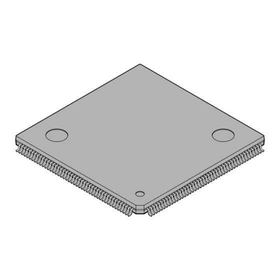
FR60 32-BIT MICROCONTROLLER
Brand:
Fujitsu
| Category:
Controller
| Size: 4.5 MB
Table of Contents
Table of Contents
11
Chapter 1 Overview
23
Features
24
Block Diagram
29
External Dimensions
30
Pin Layout
31
List of Pin Functions
32
Input-Output Circuit Forms
39
Chapter 2 Handling the Device
45
Precautions on Handling the Device
46
Chapter 3 Cpu and Control Units
51
Memory Space
52
Internal Architecture
53
Programming Model
58
Data Configuration
65
Word Alignment
66
Memory Map
67
Branch Instructions
68
EIT (Exception, Interrupt, and Trap)
71
EIT Interrupt Levels
72
Interrupt Control Unit (ICR)
74
System Stack Pointer (SSP)
75
Table Base Register (TBR)
76
Multiple EIT Processing
80
EIT Operations
82
Operating Modes
86
Reset (Device Initialization)
89
Reset Levels
90
Reset Sources
91
Reset Sequence
93
Oscillation Stabilization Wait Time
94
Reset Operation Modes
96
Clock Generation Control
97
PLL Controls
98
Oscillation Stabilization Wait Time and PLL Lock Wait Time
100
Clock Distribution
102
Clock Division
104
Block Diagram of Clock Generation Controller
105
Register of Clock Generation Controller
106
Peripheral Circuits of Clock Controller
122
Device State Control
126
Device States and State Transitions
127
Low-Power Modes
132
Watch Timer
136
Main Clock Oscillation Stabilization Wait Timer
142
Chapter 4 I/O Port
149
Overview of the I/O Port
150
I/O Port Registers
152
Chapter 5 16-Bit Reload Timer
159
Overview of the 16-Bit Reload Timer
160
16-Bit Reload Timer Registers
161
Control Status Register (TMCSR)
162
16-Bit Timer Register (TMR)
165
16-Bit Reload Register (TMRLR)
166
16-Bit Reload Timer Operation
167
Chapter 6 Programmable Pulse Generator (Ppg) Timer
173
Outline
174
Block Diagram of the PPG Timer
175
Registers of the PPG Timer
177
Control Status Register (PCNH, PCNL)
178
PPG Cycle Setting Register (PCSR)
181
PPG Duty Setting Register (PDUT)
182
PPG Timer Register (PTMR)
183
PWM Mode
184
One-Shot Mode
186
Interrupts
188
PPG Output of ALL-L and ALL-H
189
Precautions on Using the PPG Timer
190
Chapter 7 Multifunction Timer
191
Overview of the Multifunction Timer
192
Registers of the Multifunction Timer
194
Low-Pass Filter Control Register (Txlpcr)
195
Capture Control Register (Txccr)
196
Timer Setting Register (Txtcr)
198
Entire Timer Control Register (Txr)
200
Timer Compare Data Register (Txdrr)
201
Capture Data Register (Txcrr)
202
Test Mode Register (TMODE)
203
Used Bit Description for each Mode
204
Multifunction Timer Operation
206
Chapter 8 16-Bit Pulse Width Counter
211
Overview of the 16-Bit Pulse Width Counter
212
Registers of the 16-Bit Pulse Width Counter
213
PWC Control Register (PWCCL)
214
PWC Control Register (PWCCH)
216
PWC Data Register (PWCD)
218
PWC Control Register 2 (PWCC2)
219
Upper Value Setting Register (PWCUD)
220
Operation of the 16-Bit Pulse Width Counter
221
Chapter 9 Interrupt Controller
225
Overview of the Interrupt Controller
226
Interrupt Controller Registers
228
Interrupt Control Register (ICR)
230
Hold Request Cancellation Request Level Setting Register (HRCL)
232
Interrupt Controller Operation
233
Example of Using the Hold Request Cancellation Request Function (HRCR)
236
Chapter 10 External Interrupt and Nmi Controller
239
Overview of the External Interrupt and NMI Controller
240
External Interrupt and NMI Controller Registers
241
Interrupt Enable Register (ENIR)
242
External Interrupt Source Register (EIRR)
243
External Interrupt Request Level Setting Register (ELVR)
244
Operation of the External Interrupt and NMI Controller
245
Chapter 11 Realos-Related Hardware
249
Delayed Interrupt Module
250
Delayed Interrupt Module Registers
251
Operation of the Delayed Interrupt Module
252
Bit Search Module
253
Bit Search Module Registers
254
Bit Search Module Operation
257
Chapter 12 10-Bit A/D Converter
262
Overview of the 10-Bit A/D Converter
262
Registers of the 10-Bit A/D Converter
263
A/DC Control Register (ADCTH, ADCTL)
264
Software Conversion Analog Input Select Register
266
A/D Conversion Result Register (Channels 0 to 9)
267
A/D Converter Test Register
268
Operation of the 10-Bit A/D Converter
269
Chapter 13 U-Timer
271
Overview
272
U-TIMER Registers
273
U-TIMER Operation
276
Chapter 14 Uart
277
Overview of the UART
278
UART Registers
280
Serial Mode Register (SMR)
281
Serial Control Register (SCR)
283
Serial Input Data Register (Sidr)/Serial Output Data Register (SODR)
286
Serial Status Register (SSR)
287
UART Operation
291
Asynchronous (Start-Stop Synchronization) Mode
293
Clock Synchronous Mode
294
Occurrence of Interrupts and Timing for Setting Flags
296
Example of Using the UART
299
Example of Setting U-TIMER Baud Rates and Reload Values
301
Chapter 15 I 2 C Interface
303
Overview of the I 2 C Interface
304
I 2 C Interface Registers
309
Bus Status Register (IBSR)
311
Bus Control Register (IBCR)
314
Clock Control Register (ICCR)
320
10-Bit Slave Address Register (ITBA)
322
10-Bit Slave Address Mask Register (ITMK)
323
7-Bit Slave Address Register (ISBA)
325
7-Bit Slave Address Mask Register (ISMK)
326
Data Register (IDAR)
327
Clock Disable Register (IDBL)
328
I 2 C Interface Operation
332
Operation Flowcharts
337
Chapter 16 Dma Controller (Dmac)
341
Overview of the DMA Controller (DMAC)
342
DMA Controller (DMAC) Registers
344
Control/Status Registers a (DMACA0 to DMACA4)
346
Control/Status Registers B (DMACB0 to DMACB4)
351
Transfer Source/Transfer Destination Address Setting Registers (DMASA0 to 4/DMADA0 to 4)
358
All-Channel Control Register (DMACR)
360
Other Functions
362
DMA Controller Operation
363
Setting a Transfer Request
366
Transfer Sequence
368
General Aspects of DMA Transfer
373
Addressing Mode
375
Data Types
376
Transfer Count Control
377
CPU Control
378
Hold Arbitration
379
Operation from Starting to End/Stopping
380
16.3.10 DMAC Interrupt Control
384
16.3.11 Channel Selection and Control
385
Supplement on External Pin and Internal Operation Timing
387
Operation Flowcharts
392
Data Bus
395
Chapter 17 Usb Function
399
Overview of the USB Function
400
USB Interface Registers
403
Data Transmission Registers (for End Points)
406
Status Registers
409
Control Registers
416
Operation of the USB Function
431
Flow of Data Transfer
432
CPU Access Operation
438
Interrupt Sources
445
Setting of End Point Buffer
446
Examples of Software Control
448
Supplementary Notes on the USB Function
457
Double Buffer
458
Controlling the D+ Terminating Resistor on the Board
463
Automatic Response of Macro Program to USB Standard Request Commands
464
USB Function Macro Program Operation in the Default Status
466
USB Clock Control in the Suspended Status
467
Detection of USB Connector Connection and Disconnection
468
Accuracy of UCLK48
469
Setting of Transfer Enable Bit (BFOK) During Control Transfer
470
Precautions for Control Transfer
471
17.4.10 Macro Program Status after USB Bus Reset
473
Chapter 18 Osdc
475
On-Screen Display Controller (Osdc)
476
Features
477
Block Diagram
479
Display Functions
480
Screen Configuration
481
Screen Display Modes
484
Screen Output Control
486
Screen Display Position Control
487
Display Memory (VRAM) Configuration
498
Writing to Display Memory (VRAM)
499
Palette Configuration
502
Character Display
503
18.2.10 Character Background Display
537
18.2.11 Line Background Display
546
18.2.12 Screen Background Display
555
18.2.13 Sprite Character Display
560
Control Functions
564
Dot Clock Control
565
Sync Signal Input
570
Display Signal Output
578
Display Period Control
581
Synchronization Control
583
Interrupt Control
586
OSDC Operation Control
589
Display Control Commands
591
List of Display Control Commands
592
VRAM Write Address Set (Command 0)
594
Character Data Set (Commands 1 and 2)
595
Line Control Data Set (Commands 3 and 4)
597
Screen Output Control (Commands 5-00 and 5-1)
599
Display Position Control (Commands 5-2 and 5-3)
601
Character Vertical Size Control (Command 6-0)
602
Shaded Background Frame Color Control (Command 6-1)
603
Transparent/Translucent Color Control (Command 6-2)
604
Graphic Color Control (Command 6-3)
605
Screen Background Character Control (Commands 7-1 and 7-3)
607
Sprite Character Control (Commands 8-1, 8-2, 9-0 and 9-1)
609
Synchronization Control (Command 11-0)
612
I/O Pin Control (Commands 13-0 and 13-1)
613
Display Period Control (Commands 14-0 to 14-3)
615
Interrupt Control (Command 15-0)
618
Palette Control (Commands 16-0 to 16-15)
619
OSDC Operation Control (Commands 17-0 and 17-1)
621
PLLA Clock Control (Commands 18-0 to 18-3)
623
PLLB Clock Control (Commands 18-4 to 18-7)
625
PLLC Clock Control (Commands 18-8 to 18-11)
627
Clock Selection Control (Commands 18-12 to 18-13)
629
Display Control Command (CC)
631
CC Screen and Display Control Command List
632
VRAM Write Address Setting (Command 0)
633
Character Data Setting (Command 1, Command 2)
634
Line Control Data Setting (Command 3, Command 4)
636
Display Output Control (Command 5-00, Command 5-1)
638
Display Position Control (Command 5-2, Command 5-3)
640
Character Vertical Size Control (Command 6-0)
641
Transparent Color Control (Command 6-2)
642
Display Period Control (Command 14-0, 14-1, 14-2, 14-3)
643
Interrupt Control (Command 15-0)
645
Palette Control (Command 16-0 to Command 16-15)
646
FONT RAM Interface
647
Chapter 19 Flash Memory
651
Outline of Flash Memory
652
Flash Memory Registers
659
Flash Control/Status Register (FLCR)
660
Flash Memory Wait Register (FLWC)
662
Flash Memory Access Modes
664
Automatic Algorithm of Flash Memory
666
Execution Status of the Automatic Algorithm
670
Writing to and Erasing from Flash Memory
675
Read/Reset Status
676
Data Writing
677
Data Erasure (Chip Erasure)
679
Data Erasure (Sector Erasure)
680
Temporary Sector Erase Stop
682
Sector Erase Restart
683
Chapter 20 Serial Programming Connection
685
Serial Programming Connection
686
Appendix
691
APPENDIX A I/O Map
692
APPENDIX B Interrupt Vector
707
APPENDIX C Dot Clock Generation PLL
710
APPENDIX D USB Clock
712
APPENDIX E Macro Reset
713
APPENDIX F USB Low-Power Consumption Mode
714
APPENDIX G External Bus Interface Setting
715
APPENDIX H Pin State List
717
APPENDIX I Instruction Lists
721
How to Read the Instruction Lists
722
FR Family Instruction Lists
726
Index
743
Advertisement
Advertisement
Related Products
Fujitsu MB90390 Series
Fujitsu MB86617A
Fujitsu MB3788
Fujitsu MB86292 Orchid
Fujitsu MB86291 Scarlet
Fujitsu MB2146-410-01-E
Fujitsu MB91360 SERIES
Fujitsu MB91350A Series
Fujitsu MB91F467C
Fujitsu MB91V360
Fujitsu Categories
Air Conditioner
Laptop
Server
Scanner
Storage
More Fujitsu Manuals
Login
Sign In
OR
Sign in with Facebook
Sign in with Google
Upload manual
Upload from disk
Upload from URL