
Related Manuals for Mitsubishi Electric Q64AD2DA


Summary of Contents for Mitsubishi Electric Q64AD2DA
- Page 1 Analog Input/Output Module User's Manual -Q64AD2DA -GX Configurator-AD (SW2D5C-QADU-E) -GX Configurator-DA (SW2D5C-QDAU-E)
-
Page 3: Safety Precautions
SAFETY PRECAUTIONS (Read these precautions before using this product.) Before using this product, please read this manual and the relevant manuals carefully and pay full attention to safety to handle the product correctly. The precautions given in this manual are concerned with this product only. For the safety precautions of the programmable controller system, refer to the user’s manual for the CPU module used. - Page 4 [Installation Precautions] CAUTION Use the programmable controller in an environment that meets the general specifications in the user’s manual for the CPU module used. Failure to do so may result in electric shock, fire, malfunction, or damage to or deterioration of the product.
- Page 5 [Wiring Precautions] CAUTION Ground the FG terminal to the protective ground conductor dedicated to the programmable controller. Failure to do so may result in electric shock or malfunction. After wiring, attach the included terminal cover to the module before turning it on for operation. Failure to do so may result in electric shock.
- Page 6 [Wiring Precautions] CAUTION A protective film is attached to the top of the module to prevent foreign matter, such as wire chips, from entering the module during wiring. Do not remove the film during wiring. Remove it for heat dissipation before system operation. [Startup and Maintenance Precautions] CAUTION Do not disassemble or modify the modules.
-
Page 7: Conditions Of Use For The Product
CONDITIONS OF USE FOR THE PRODUCT (1) Mitsubishi programmable controller ("the PRODUCT") shall be used in conditions; i) where any problem, fault or failure occurring in the PRODUCT, if any, shall not lead to any major or serious accident; and ii) where the backup and fail-safe function are systematically or automatically provided outside of the PRODUCT for the case of any problem, fault or failure occurring in the PRODUCT. -
Page 8: Revisions
This manual confers no industrial property rights or any rights of any other kind, nor does it confer any patent licenses. Mitsubishi Electric Corporation cannot be held responsible for any problems involving industrial property rights which may occur as a result of using the contents noted in this manual. -
Page 9: Table Of Contents
CHAPTER2 SYSTEM CONFIGURATION 2 - 1 to 2 - 7 Applicable Systems ......................... 2 - 1 Using the Q64AD2DA with Redundant CPU ................... 2 - 4 Checking Function Version, Serial Number, and Software Version ..........2 - 5 CHAPTER3 SPECIFICATIONS 3 - 1 to 3 - 11 Performance Specifications ...................... - Page 10 Function Details of D/A Conversion ....................4 - 25 4.3.1 D/A output enable/disable function ..................4 - 25 4.3.2 Analog output HOLD/CLEAR function ..................4 - 25 4.3.3 Analog output test during a CPU module STOP..............4 - 27 4.3.4 Scaling function (D/A conversion)...................
- Page 11 6.23 CH1 Input Signal Error Detection Flag (Un\G114)................. 6 - 25 6.24 CH1 Oldest Pointer (Un\G120) ...................... 6 - 26 6.25 CH1 Latest Pointer (Un\G121)....................... 6 - 27 6.26 CH1 Logging Data Points (Un\G122) .................... 6 - 28 6.27 CH1 Trigger Pointer (Un\G123) ..................... 6 - 28 6.28 CH1 Latest Error Code (Un\G190), CH1 Error Time (Un\G191 to Un\G194), Latest Error Code (Un\G1790), and Error Time (Un\G1791 to Un\G1794)..............
- Page 12 When A/D conversion completed flag does not turn on during use in normal mode ....11 - 7 11.2.6 When an analog output value is not output ................11 - 7 11.2.7 When External power off flag (X6) turns on................11 - 8 11.2.8 Checking the Q64AD2DA status .................... 11 - 9 - 10...
-
Page 13: Index - 1 To Index
APPENDIX App - 1 to App - 2 Appendix 1 External Dimensions......................App - 1 INDEX Index - 1 to Index - 2 - 11... -
Page 14: About Manuals
ABOUT MANUALS The following manuals are also related to this product. Order each manual as needed, referring to the following list. Relevant Manuals Manual number Manual name (model code) GX Developer Version 8 Operating Manual Describes the methods for creating, printing, monitoring, and debugging programs with GX SH-080373E Developer. -
Page 15: Generic Terms And Abbreviations
Generic term/ Description abbreviation Q64AD2DA Abbreviation for the Q64AD2DA analog input/output module GX Developer Product name of the software package for the MELSEC programmable controllers GX Works2 Abbreviation for analog-digital converter module setting and monitor tool, GX Configurator- GX Configurator-AD... -
Page 16: Packing List
7 (64-bit version)" indicates the 64-bit version only. PACKING LIST The following is included in the package. Model Product name Quantity Q64AD2DA analog input/output module Q64AD2DA External power supply connector SW2D5C-QADU-E GX Configurator-AD Version 2 (Single license product) (CD-ROM) SW2D5C-QADU-EA... -
Page 17: Chapter1 Overview
CHAPTER1 OVERVIEW This user's manual provides the specifications, handling instructions, programming procedures, and other information of the Q64AD2DA analog input/output module (hereinafter the "Q64AD2DA"), which is designed to use with the MELSEC-Q series CPU module. Features (1) Analog input and output using a module The Q64AD2DA can perform both A/D conversion using four channels and D/A conversion using two channels. - Page 18 * 1 Either GX Configurator-AD or GX Configurator-DA checks the intelligent function module parameter setting and the setting status or operation status of the Q64AD2DA. In addition, the setting and status can be checked by installing both GX Configurator-AD and GX Configurator-DA.
-
Page 19: Chapter2 System Configuration
Q64AD2DA, refer to the Q Corresponding MELSECNET/H Network System Reference Manual (Remote I/O network). (2) Support of multiple CPU system When using the Q64AD2DA in a multiple CPU system, refer to the following manual first. • QCPU User's Manual (Multiple CPU System) (3) Support of online module change The function version of the Q64AD2DA has been "C"... - Page 20 SYSTEM CONFIGURATION (4) Supported software packages Operating the Q64AD2DA requires GX developer or GX Works2 with a software version that is compatible with the CPU system used. The software packages, GX Configurator-AD and GX Configurator-DA , are not required. The intelligent function module parameter setting, setting status, and operating status can be checked easily by using the packages.
- Page 21 (1) Depending on the version of GX Configurator-AD or GX Configurator-DA, supported systems and CPU modules, and available functions of the Q64AD2DA vary. (2) When using GX Works2, refer to the following: • GX Works2 Version 1 Operating Manual (Common) •...
-
Page 22: Using The Q64Ad2Da With Redundant Cpu
Connecting to a programmable controller CPU via an intelligent function module (Ethernet module, MELSECNET/H module, or CC-Link module) on the main base unit Figure 2.1 Communication path for GX Configurator-AD and GX Configurator-DA 2.2 Using the Q64AD2DA with Redundant CPU... -
Page 23: Checking Function Version, Serial Number, And Software Version
Checking Function Version, Serial Number, and Software Version This section describes how to check the function version of the Q64AD2DA and the software version of GX Configurator-AD or GX Configurator-DA. (1) Checking the function version and serial number of the Q64AD2DA... - Page 24 SYSTEM CONFIGURATION (c) Checking on the System monitor dialog box (Product Information List) To display the system monitor, select [Diagnostics] [System monitor] and click Product Information List button of GX Developer. Function version Serial No. Product No. Figure 2.4 Checking the serial number and function version POINT The serial number displayed on the Product information list dialog box of GX Developer may differ from that on the rating plate and on the front of the module.
- Page 25 SYSTEM CONFIGURATION (2) Checking the software version of GX Configurator-AD and GX Configurator-DA To check the software version of GX Configurator-AD and GX Configurator-DA, select [Help] [Product information] of GX Developer. Software version ("Product information" dialog box of GX Developer Version 8) Figure 2.5 Product information dialog box 2.3 Checking Function Version, Serial Number, and Software Version...
-
Page 26: Chapter3 Specifications
SPECIFICATIONS CHAPTER3 SPECIFICATIONS Performance Specifications The following table shows the performance specifications of the Q64AD2DA. Table 3.1 Performance specifications of the Q64AD2DA (1/2) Item Specifications Number of analog input 4 channels points Analog Voltage -10 to 10VDC (Input resistance: 1M ) - Page 27 SPECIFICATIONS Table 3.1 Performance specifications of the Q64AD2DA (2/2) Item Specifications Number of analog output 2 channels points Normal resolution mode: -96 to 4095, -4096 to 4095 Digital input High resolution mode: -288 to 12287, -16384 to 16383 Analog Voltage...
- Page 28 Screw tightening torque 0.5 to 0.6N m External power supply connector (accessory) Figure 3.1 When inserting two cables into one terminal Remark For general specifications of the Q64AD2DA, refer to the user's manual for the CPU module used. 3.1 Performance Specifications...
-
Page 29: I/O Conversion Characteristic
SPECIFICATIONS I/O Conversion Characteristic 3.2.1 I/O conversion characteristic of A/D conversion The I/O conversion characteristic of A/D conversion represents the angle formed by a straight line connecting the "offset value" and "gain value" when the analog signals (voltage or current input) from outside the programmable controller are converted to digital values. - Page 30 SPECIFICATIONS (1) Voltage input characteristic Figure 3.2 shows voltage input characteristics. 2) 0 to 5V 1) 1 to 5V Practical analog input range Practical analog input range High resolution High resolution mode mode 12287 12287 12000 12000 Normal resolution Normal resolution mode mode 4095...
- Page 31 SPECIFICATIONS POINT (1) Set each input range within the practical analog input range and digital output range. If these ranges are exceeded, the maximum resolution and accuracy may not fall within the performance specifications. (Avoid using the dotted line area shown in Figure 3.2.) (2) Do not input an analog input voltage of 15 V or more.
- Page 32 SPECIFICATIONS (2) Current input characteristic Figure 3.3 shows current input characteristics. 1) 4 to 20mA Practical analog input range 2) 0 to 20mA Practical analog input range High resolution High resolution mode mode 12287 12287 12000 12000 Normal resolution Normal resolution mode mode 4095...
- Page 33 SPECIFICATIONS POINT (1) Set each input range within the practical analog input range and digital output range. If these ranges are exceeded, the maximum resolution and accuracy may not fall within the performance specifications. (Avoid using the dotted line area shown in Figure 3.3.) (2) Do not input an analog input current of 30 mA or more.
-
Page 34: I/O Conversion Characteristic Of D/A Conversion
SPECIFICATIONS 3.2.2 I/O conversion characteristic of D/A conversion The I/O conversion characteristic of D/A conversion represents the angle formed by a straight line connecting the "offset value" and "gain value" when converting the digital input value written from the CPU module to an analog output value (voltage or current output). [Offset value] The offset value refers to the analog output value (voltage or current) when the digital input value set from the CPU module is 0. - Page 35 SPECIFICATIONS (1) Voltage output characteristic Figure 3.4 shows voltage output characteristics. 1) 1 to 5V 2) 0 to 5V Normal resolution Normal resolution mode mode High resolution High resolution mode mode -288 -96 4000 4095 12000 12287 -288 -96 4000 4095 12000 12287 Digital input value Digital input value 3) -10 to 10V...
- Page 36 SPECIFICATIONS (2) Current output characteristic Figure 3.5 shows current output characteristics. 2) 0 to 20mA 1) 4 to 20mA Normal resolution Normal resolution mode mode High resolution High resolution mode mode -288 -96 4000 4095 12000 12287 -288 -96 4000 4095 12000 12287 Digital input value Digital input value...
-
Page 37: Chapter4 Function
CH5.) For the device numbers and buffer memory addresses used for other channels, refer to Section 5.1 and Section 6.1. Function List Table 4.1 lists the functions of the Q64AD2DA. Table 4.1 Function list Reference Item... - Page 38 FUNCTION Table 4.1 Function list Reference Item Function section This function sets whether D/A conversion values are output or offset values are output for each channel. D/A output enable/disable Section function 4.3.1 The conversion speed does not change regardless of whether CH5 Output enable/disable flag (Y5) is enabled (ON) or disabled (OFF).
-
Page 39: Function Details Of A/D Conversion
(1) Sampling period of the Q64AD2DA A/D conversion is performed from CH1 to CH4 and D/A conversion is performed from CH5 to CH6 in series in 500 s per channel for the Q64AD2DA. Sampling period is the period of renewing digital output values. - Page 40 FUNCTION POINT Set the setting time that meets the following condition for time averaging processing. If the setting time does not meet the following condition, an error (error code: 202) occurs and the digital output value changes to 0. • Setting time Minimum processing times 4 (times) 0.5(ms) Number...
- Page 41 FUNCTION (c) Moving average The digital output values imported per sampling period are averaged to find a value, which is then stored into the buffer memory. Since average processing is made with data shifted per sampling, the most recent digital output value is obtainable. Sampling period A/D conversion value 16000...
-
Page 42: Maximum And Minimum Values Hold Function
FUNCTION 4.2.2 Maximum and minimum values hold function The maximum and minimum digital output value and scaling value are held in the buffer memory for each channel. (1) Setting methods (a) The maximum and minimum values are stored into the following buffer memory when conversions start. - Page 43 FUNCTION (2) Setting methods 1) Set the buffer memory as follows: • Setting CH1 A/D conversion scaling enable/disable setting (Un\G10) to be enabled (0). • Setting a value corresponding to the upper limit of digital output as the scaling upper limit value set with CH1 A/D conversion scaling upper limit value (Un\G12).
- Page 44 FUNCTION (3) How to calculate a scaling value Input range: 0 to 10V, 0 to 5V, 1 to 5V, 0 to 20mA, and 4 to 20mA Scaling value = Input range: -10 to 10V Scaling value = Max - : CH1 Digital output value (Un/G100) : The maximum digital output value in the input range being used : The minimum digital output value in the input range being used : CH1 A/D conversion scaling upper limit value (Un\G12)
-
Page 45: Shifting Function (A/D Conversion)
FUNCTION 4.2.4 Shifting function (A/D conversion) The shifting function adds a setting quantity to a digital output value (shifting a digital output value) and stores the value into buffer memory. (1) Overview (a) The shifted output values are stored into CH1 Scaling value (Un\G102). (b) The shifting amount to conversion value can be set within the range from -32768 to 32767. - Page 46 FUNCTION (3) Setting example For the channel in setting the input range to 0 to 5V and the high resolution mode (to 0 to 12000), I/O characteristic is adjusted as shown below. 1) CH1 Digital output value 12000 2) Scaling value (Un\G100) 11990 (After adjustment)
-
Page 47: Input Signal Error Detection Function
FUNCTION 4.2.5 Input signal error detection function Input signal error detection function is the function that detects voltage or current input exceeding a setting range. (1) Overview (a) If the input voltage or current rises to or above the input signal error detection upper limit value or falls to or below the lower limit value, an error occurs under the following operations. - Page 48 FUNCTION (e) The input signal error detection is executed at every sampling processing. (f) The condition of the input signal error detection can be set with CH1 Input signal error detection setting (Un\G20). The conditions of the input signal error detection are described in the table below. Table 4.2 Condition of input signal error detection and operation CH1 Input signal error Condition of input signal error detection...
- Page 49 FUNCTION (2) Setting methods 1) Set the value for CH1 Input signal error detection setting value (Un\G21) of corresponding channels in 0.1% increments. 2) Set the value for CH1 A/D conversion enable/disable setting (Un\G0) of corresponding channels to A/D conversion enable (0). 3) Select the condition of input signal error detection to be used from 1 to 3 in the Table 4.2 for CH1 Input signal error detection setting (Un\G20) of corresponding channels.
- Page 50 FUNCTION The following table shows lower limit values, offset values, and gain values calculated in setting input ranges. Table 4.3 Lower limit values, offset values, and gain values calculated by setting input ranges Input Analog input range Lower limit value Offset value Gain value 0 to 10V...
- Page 51 FUNCTION (b) Set CH1 Input signal error detection setting (Un\G20) in the lower detection (2). In this case, the value for CH1 Input signal error detection operates as below. (An error is detected while Upper Input signal error detection and lower detection (1) is set.) upper limit value 21.6mA 1.6mA...
-
Page 52: Input Range Extended Mode Function
FUNCTION 4.2.6 Input range extended mode function The input range extended mode function is the function increasing the input range of 4 to 20mA and 1 to 5V. Table 4.4 Input range and digital output value for extended mode Normal mode Extended mode CH1 Digital output value Increased... - Page 53 FUNCTION (3) Disconnection detection Combining the input range extended mode function and input signal error detection function detects a disconnection. If the input analog current value changes to 2mA or less, or the input analog voltage value changes 0.5V or less, an external wiring is disconnected, and CH1 Input signal error detection flag (Un\G114) is set to on (1).
-
Page 54: Logging Function
Logging data can be stored up to 10000th data point area for a channel. The stored data are retained until when the CPU module is powered off or Operating condition setting request (Y9) is set to on. Q64AD2DA Logging data storage area Specified device data... - Page 55 FUNCTION (3) Logging start To use a logging facility, the following items are required for the initial setting. Start Initial setting performed by users Set the following items. Logging enable/disable setting Logging data setting Logging cycle setting value Logging cycle unit setting Logging points after trigger Logging hold request signal...
- Page 56 Hold trigger is the trigger that occurs for the case of preset trigger conditions to be met when a logging facility is used. When the Q64AD2DA detects a hold trigger, the logging facility stops (hold) collecting logging data after logging the number of preset points.
- Page 57 FUNCTION CH1 Logging hold request (Y1) Trigger condition enable/disable Disable Enable (waiting for trigger condition) Satisfied Trigger condition satisfied/not satisfied*1 Not satisfied Hold trigger occurred Logging hold CH1 Logging data storage area Data stored before latest (Un\G5000 to Un\G14999) 10000 are discarded. Logging points after trigger (Un\G34) Logging data points (Un\G122)
- Page 58 FUNCTION POINT (1) If logging does not start, check the following: • Is CH1 Logging enable/disable setting (Un\G30) set to be disabled (1)? If CH1 Logging enable/disable setting (Un\G30) has been set to be disabled (1), set CH1 Logging enable/disable setting (Un\G30) to be enabled (0), •...
- Page 59 FUNCTION (4) Reference of logging data If CH1 Logging hold flag (X1) is set to on, refer to the buffer memory shown in Figure 4.13 and Figure 4.14. The logging datad point determines how to refer to the logging data storage area. [Example] The held logging data point is 10000.
- Page 60 (2) From when CH1 Logging hold request (Y1) is set to on until when a hold trigger occurs in the Q64AD2DA, the delay is up to the time calculated as shown below. • Trigger occurrence delay...
-
Page 61: Function Details Of D/A Conversion
* 1 This occurs when program operations are not completed within the scheduled time due to a hardware problem of the Q64AD2DA. When a watchdog timer error occurs, Module ready (X0) is set to off and the Q64AD2DA RUN LED is turned off. - Page 62 • Validate the station unit block guarantee of the send side cyclic data. • The setting for holding the Q64AD2DA output in the case of a link error must be made in the "Error time output mode in the I/O assignment setting".
-
Page 63: Analog Output Test During A Cpu Module Stop
FUNCTION 4.3.3 Analog output test during a CPU module STOP While the CPU module is in stop status, an analog output test as shown can be performed. (Refer to Table 4.13.) (1) Operating method To conduct an analog output test, perform the following on Device test of GX Developer, on the relevant test screens of Configurator-AD, or Configurator-DA. -
Page 64: Scaling Function (D/A Conversion)
FUNCTION 4.3.4 Scaling function (D/A conversion) This function changes an input range of digital input values to a given range between - 32000 and 32000. (1) Overview (a) Whether using the scaling function (D/A conversion) for each channel or not can be specified with CH5 D/A conversion scaling enable/disable setting (Un\G810). - Page 65 FUNCTION [Setting example] Using the scaling function (D/A conversion) in input range from -10 to 10V and high resolution mode (from -16000 to 16000) (a) Setting value • CH5 D/A conversion scaling upper limit value (Un\G812) S : 14000 • CH5 D/A conversion scaling lower limit value (Un\G811) S : 2000 (b) Input value Digital input value Dx: 7000...
- Page 66 FUNCTION As indicated in the formula of (4) in this section or Figure 4.16, the value exceeding the D/A conversion scaling upper limit or the value that falls below the D/A conversion lower limit can be set for a digital input value. However, the analog output value corresponding to the real conversion digital value, exceeding the range cannot be ensured.
-
Page 67: Shifting Function (D/A Conversion)
FUNCTION 4.3.5 Shifting function (D/A conversion) The shifting function adds a setting quantity to a digital input value (shifting a analog output value). (1) Overview • The shifting amount to input value can be set within the range from -32768 to 32767. - Page 68 FUNCTION (3) Setting example For the channel in setting the output range to 0 to 20mA and the high resolution mode (to 0 to 4000), I/O characteristic is adjusted as shown below. Analog output value Input value shift amount 20.1mA 20.0mA Before adjustment...
-
Page 69: Details Of Common Function
The Q64AD2DA conversion speed is calculated with the formula, 500 s Number of conversion enabled channels. The Q64AD2DA converts according to the two types of the conversion sequence, group 1 and group 2. Table 4.18 Conversion sequence of A/D conversion channels and D/A conversion channels... -
Page 70: Chapter5 I/O Signals For The Cpu Module
Table 5.1 lists the I/O signals of the Q64AD2DA. Note that I/O numbers (X/Y) shown in this chapter and thereafter are the values when the start I/O number for the Q64AD2DA is set to 0. Table 5.1 List of I/O signal... -
Page 71: Details Of I/O Signals
I/O SIGNALS FOR THE CPU MODULE Details of I/O Signals I/O signals for the Q64AD2DA are explained in detail below. Device numbers (X/Y) and buffer memory address shown in this chapter are for CH1 (the device number and buffer memory address used only for the D/A conversion are CH5.). - Page 72 (a) If the logging is held, CH1 Logging hold flag (X1) will be set to on. The following shows the timing for the logging to be held. 1) A hold trigger detection with Logging hold request signal Executed with the Q64AD2DA CH1 Logging hold request (Y1) Hold trigger...
- Page 73 If not, External power off flag (X6) may be set to on. (f) When the external power supply is turned on after the CPU module is powered on, the timing diagram is as follows: Executed with the Q64AD2DA Executed with sequence program Programmable controller...
- Page 74 (d) After the first updating, the value 1 (first A/D conversion completed) will be stored into CH1 A/D conversion completed flag (Un\G113) again. The averaging processing will start from the first time after resumption of A/D conversion. Executed with the Q64AD2DA Executed with sequence program CH1 Input signal error Input signal error detection...
- Page 75 (c) Under the following conditions, Operating condition setting completed flag (X9) will be set to off. • When Operating condition setting request (Y9) is set to on Executed with the Q64AD2DA Executed with sequence program Module ready (X0) Operating condition setting...
- Page 76 * 1 Not relevant to the channels that D/A conversion is enabled (b) If the external power supply for the Q64AD2DA turns off, A/D conversion completed flag (XE) will flow as shown in the section of External power off flag (X6).
- Page 77 (a) If a write error occurs, Error flag (XF) will be set to on. (b) To clear the error code, set Error clear request (YF) to on. Executed with the Q64AD2DA Executed with sequence program CH1 Latest error code (Un\G190)
-
Page 78: Output Signals
I/O SIGNALS FOR THE CPU MODULE 5.2.2 Output signals (1) CH1 Logging hold request (Y1) For information on the output signals for CH2 or later channels, refer to Section 5.1. (a) If the level trigger condition setting using CH1 Level trigger condition setting (Un\G35) is "Disable"... - Page 79 I/O SIGNALS FOR THE CPU MODULE (3) Operating condition setting request (Y9) (a) Set this signal to on when making any of the following buffer memory valid. • CH1 A/D conversion enable/disable setting (Un\G0) • CH5 D/A conversion enable/disable setting (Un\G800) •...
-
Page 80: Chapter6 Buffer Memory
BUFFER MEMORY Buffer Memory Assignment This section explains the buffer memory assignments of the Q64AD2DA. Device numbers (X/Y) and buffer memory address shown in the Section 6.2 and later sections are for CH1 (the device number and buffer memory address used only for the D/ A conversion are CH5.). - Page 81 BUFFER MEMORY Table 6.1 A/D conversion area (Un\G0 to Un\G799) Address (decimal) Data Item Description Default Read/write type System area Digital output value System area Scaling value System area Maximum digital output value System area Minimum digital output value System area Maximum scaling value System area Minimum scaling value...
- Page 82 BUFFER MEMORY (2) D/A conversion area (Un\G800 to Un\G1199) Table 6.2 D/A conversion area (Un\G800 to Un\G1199) Address (decimal) Data Item Description Default Read/write type 1000 D/A conversion enable/disable setting 1001 System area 1002 Digital input value 1003 System area 1009 1010 D/A conversion scaling enable/disable setting...
- Page 83 BUFFER MEMORY (3) Common area (Un\G1200 to Un\G1799) Table 6.3 Common area (Un\G1200 to Un\G1799) Data Item Address (decimal) Description Default Read/write type 1200 System area 1599 1600 Level data 0 1601 Level data 1 1602 Level data 2 1603 Level data 3 1604 Level data 4...
- Page 84 BUFFER MEMORY Table 6.3 Common area (Un\G1200 to Un\G1799) Data Item Address (decimal) Description Default Read/write type 1764 CH5 Set value check code 1765 CH6 Set value check code 1766 System area 1773 1774 CH5 Real conversion digital value 1775 CH6 Real conversion digital value 1776 System area...
- Page 85 BUFFER MEMORY (4) Error history (Un\G1800 to Un\G1964) Table 6.4 Error history (Un\G1800 to Un\G1964) Data Item Address (decimal) History number Description Default Read/write type 1800 Latest address of error history 1801 System area 1809 1810 Error code First two digits Last two digits of 1811 of the year...
- Page 86 BUFFER MEMORY Table 6.4 Error history (Un\G1800 to Un\G1964) Data Item Address (decimal) History number Description Default Read/write type 1860 Error code First two digits Last two digits of 1861 of the year the year History 6 1862 Month Error time 1863 Hour Minute...
- Page 87 BUFFER MEMORY Table 6.4 Error history (Un\G1800 to Un\G1964) Data Item Address (decimal) History number Description Default Read/write type 1915 System area 1919 1920 Error code First two digits Last two digits of 1921 of the year the year History 12 1922 Month Error time...
- Page 88 BUFFER MEMORY (5) Logging area (Un\G5000 to Un\G49999) Table 6.5 Logging area (Un\G5000 to Un\G49999) Data Item Address (decimal) Description Default Read/write type 5000 CH1 Logging data 14999 15000 CH2 Logging data 24999 25000 Logging CH3 Logging data area 34999 35000 CH4 Logging data 44999...
-
Page 89: Ch1 A/D Conversion Enable/Disable Setting (Un\G0)
BUFFER MEMORY CH1 A/D Conversion Enable/Disable Setting (Un\G0) Whether to enable or disable A/D conversion is set. For information on the buffer memory for CH2 or later channels, refer to Section 6.1 (1). (1) Setting method (a) Set A/D conversion enable/disable setting by using the buffer memory. Table 6.6 Setting range of CH1 A/D conversion enable/disable setting (Un\G0) Setting value Description... -
Page 90: Ch1 Averaging Process (Time/Number Of Times) Setting (Un\G2)
BUFFER MEMORY CH1 Averaging Process (Time/Number of Times) Setting (Un\G2) If the averaging processing (1 to 3) is set, set an amount of time or number of times by using CH1 Averaging process method setting (Un\G1). (Refer to Section 4.2.1.) For information on the buffer memory for CH2 or later, refer to Section 6.1 (1). -
Page 91: Ch1 A/D Conversion Scaling Lower Limit Value (Un\G11) And Ch1 A/D Conversion Scaling Upper Limit Value (Un\G12)
BUFFER MEMORY CH1 A/D Conversion Scaling Lower Limit Value (Un\G11) and CH1 A/D Conversion Scaling Upper Limit Value (Un\G12) A scaling range of converted digital output values is set. (Refer to Section 4.2.3.) For information on the buffer memory for CH2 or later, refer to Section 6.1 (1). (1) Setting method (a) Set an A/D scaling conversion range by using the buffer memory. -
Page 92: Ch1 Shifting Amount To Conversion Value (Un\G13)
BUFFER MEMORY CH1 Shifting Amount to Conversion Value (Un\G13) A quantity to be shifted using the shifting function (A/D conversion) is set. (Refer to Section 4.2.4.) For information on the buffer memory for CH2 or later, refer to Section 6.1 (1). (1) Setting method (a) Set a quantity to be shifted by using the buffer memory. -
Page 93: Ch1 Input Signal Error Detection Setting Value (Un\G21)
BUFFER MEMORY CH1 Input Signal Error Detection Setting Value (Un\G21) The value detecting an error of input analog values is set. (Refer to Section 4.2.5.) For information on the buffer memory for CH2 or later, refer to Section 6.1 (1). (1) Setting method (a) Set a value within the setting range by using the buffer memory. -
Page 94: Ch1 Logging Cycle Setting Value (Un\G31) And Ch1 Logging Cycle Unit Setting (Un\G32)
BUFFER MEMORY 6.11 CH1 Logging Cycle Setting Value (Un\G31) and CH1 Logging Cycle Unit Setting (Un\G32) A storing cycle of data for logging is set. (Refer to Section 4.2.7 (3).) For information on the buffer memory for CH2 or later, refer to Section 6.1 (1). (1) Setting method (a) Set a storing cycle of data by using the buffer memory. -
Page 95: Ch1 Logging Data Setting (Un\G33)
BUFFER MEMORY 6.12 CH1 Logging Data Setting (Un\G33) Data to be logged is set during the logging facility use. (Refer to Section 4.2.7 (3).) For information on the buffer memory for CH2 or later, refer to Section 6.1 (1). (1) Setting method (a) Set data to be logged by using the buffer memory. -
Page 96: Ch1 Level Trigger Condition Setting (Un\G35)
BUFFER MEMORY 6.14 CH1 Level Trigger Condition Setting (Un\G35) Conditions for using level triggers is set during the logging facility use. (Refer to Section 4.2.7 (3).) For information on the buffer memory for CH2 or later, refer to Section 6.1 (1). (1) Setting method (a) Set a condition for using a level trigger by using the buffer memory. - Page 97 BUFFER MEMORY (2) Default The level trigger condition setting is set to be made invalid (0) for all the channels (CH1 to CH4) in default configuration. POINT (1) When using the level trigger, set the level trigger condition using CH1 Level trigger condition setting (Un\G35) to meet the following variations.
-
Page 98: Ch1 Trigger Data (Un\G36)
Scaling value POINT Set adequate monitoring data such as digital output values, scaling values, and level data for trigger data. The other data settings do not guarantee the normal operation of the Q64AD2DA. [Example] Setting area ( System area 6.16 CH1 Trigger Setting Value (Un\G37) A value that makes level triggers work is set during the logging facility use. -
Page 99: Ch1 Digital Output Value (Un\G100, Un\G1700)
BUFFER MEMORY 6.17 CH1 Digital Output Value (Un\G100, Un\G1700) The A/D converted digital output value is set to store. For information on the buffer memory for CH2 or later, refer to Section 6.1 (1) and Section 6.1 (3). (1) Stored data (a) Storage form Digital values are stored into the buffer memory in 16-bit signed binary form. -
Page 100: Ch1 Scaling Value (Un\G102, Un\G1710)
BUFFER MEMORY 6.18 CH1 Scaling Value (Un\G102, Un\G1710) Scaled (for A/D conversion) and shifted (for A/D conversion) values (scaling value) using CH1 Digital output value (Un\G100) are stored. For information on the buffer memory for CH2 or later, refer to Section 6.1 (1) and Section 6.1 (3). -
Page 101: Ch1 Maximum Digital Output Value (Un\G104, Un\G1720) And Ch1 Minimum Digital Output Value (Un\G106, Un\G1721)
BUFFER MEMORY 6.19 CH1 Maximum Digital Output Value (Un\G104, Un\G1720) and CH1 Minimum Digital Output Value (Un\G106, Un\G1721) The maximum and minimum digital output values converted are stored. For information on the buffer memory for CH2 or later, refer to Section 6.1 (1) and Section 6.1 (3). -
Page 102: Ch1 Maximum Scaling Value (Un\G108, Un\G1740) And Ch1 Minimum Scaling Value
BUFFER MEMORY 6.20 CH1 Maximum Scaling Value (Un\G108, Un\G1740) and CH1 Minimum Scaling Value (Un\G110, Un\G1741) Maximum and minimum scaling values converted are stored. For information on the buffer memory for CH2 or later, refer to Section 6.1 (1) and Section 6.1 (3). -
Page 103: Ch1 Setting Range (Un\G112)
BUFFER MEMORY 6.21 CH1 Setting Range (Un\G112) Analog input range settings (in "Switch 1" of Switch setting for I/O and intelligent function module dialog box) for each analog input channel can be checked. For information on the buffer memory for CH2 or later, refer to Section 6.1 (1). (1) Stored data Table 6.18 Stored data of CH1 Setting range (Un\G112) Setting... -
Page 104: Ch1 Input Signal Error Detection Flag (Un\G114)
(a) An input signal error (1) will occur for CH1 Input signal error detection flag (Un\G114) in the following case. • The Q64AD2DA detects an analog input value being out of the range set with CH1 Input signal error detection setting value (Un\G21). -
Page 105: Ch1 Oldest Pointer (Un\G120)
BUFFER MEMORY 6.24 CH1 Oldest Pointer (Un\G120) In the logging data storage area, an address of buffer memory storing the oldest data can be checked. (Refer to Section 4.2.7 (4).) For information on the buffer memory for CH2 or later, refer to Section 6.1 (1). (1) Stored data The difference between the numeric value of the address storing the oldest data and the numeric value of the start address in the logging data storage area is stored. -
Page 106: Ch1 Latest Pointer (Un\G121)
BUFFER MEMORY 6.25 CH1 Latest Pointer (Un\G121) In the logging data storage area, an address of buffer memory storing the latest data can be checked. (Refer to Section 4.2.7 (4).) For information on the buffer memory for CH2 or later, refer to Section 6.1 (1). (1) Stored data The difference between the numeric value of the address storing the latest data and the numeric value of the start address in the logging data storage area is stored. -
Page 107: Ch1 Logging Data Points (Un\G122)
BUFFER MEMORY 6.26 CH1 Logging Data Points (Un\G122) An amount of data stored in the logging data storage area can be checked during the logging facility use. (Refer to Section 4.2.7 (4).) For information on the buffer memory for CH2 or later, refer to Section 6.1 (1). (1) Stored data (a) After data logging starts, the value of the buffer memory increases by 1 whenever new data are stored into CH1 Logging data storage area (Un\G5000 to... -
Page 108: Ch1 Latest Error Code (Un\G190), Ch1 Error Time (Un\G191 To Un\G194), Latest Error Code (Un\G1790), And Error Time (Un\G1791 To Un\G1794)
Un\G194), Latest Error Code (Un\G1790), and Error Time (Un\G1791 to Un\G1794) Latest error codes and error time detected by the Q64AD2DA can be checked. (Refer to Section 11.1.) For information on the buffer memory for CH2 or later, refer to Section 6.1 (1), Section 6.1 (2), and Section 6.1 (3). -
Page 109: Ch5 D/A Conversion Enable/Disable Setting (Un\G800)
(2) When using network modules, the error time may not be stored as follows: When using the Q64AD2DA in the MELSECNET/H remote I/O network, the time information is transferred as shown below. Therefore, the sequence of power supply for the system and the error timing may result in storing wrong information at the point of error occurrence. -
Page 110: Ch5 Digital Input Value (Un\G802)
BUFFER MEMORY 6.30 CH5 Digital Input Value (Un\G802) Digital input values are written from the CPU module as 16-bit signed binary code to perform D/A conversion. For information on the buffer memory for CH6, refer to Section 6.1 (2). (1) Setting method Set digital input values to be D/A converted to the buffer memory. -
Page 111: Ch5 D/A Conversion Scaling Enable/Disable Setting (Un\G810)
BUFFER MEMORY 6.31 CH5 D/A Conversion Scaling Enable/Disable Setting (Un\G810) Whether to enable or disable a scaling conversion of digital input values is set. (Refer to Section 4.3.4.) For information on the buffer memory for CH6, refer to Section 6.1 (2). (1) Setting method (a) Set whether to enable or disable the D/A conversion scaling by using the buffer memory. -
Page 112: Ch5 D/A Conversion Scaling Lower Limit Value (Un\G811) And Ch5 D/A Conversion Scaling Upper Limit Value (Un\G812)
BUFFER MEMORY 6.32 CH5 D/A Conversion Scaling Lower Limit Value (Un\G811) and CH5 D/A Conversion Scaling Upper Limit Value (Un\G812) A scaling range of converted digital input values is set. (Refer to Section 4.3.4.) For information on the buffer memory for CH6, refer to Section 6.1 (2). (1) Setting method (a) Set an D/A scaling conversion range by using the buffer memory. -
Page 113: Ch5 Set Value Check Code (Un\G900, Un\G1764)
BUFFER MEMORY 6.34 CH5 Set Value Check Code (Un\G900, Un\G1764) Whether digital values outside the settable range are set by using CH5 Digital input value (Un\G802) can be checked. For information on the buffer memory for CH6, refer to Section 6.1 (2) and Section 6.1 (3). (1) Stored data (a) When a digital input value outside the settable range (Refer to Section 6.30.) is set by using CH5 Digital input value (Un\G802), one of the check codes listed in... -
Page 114: Ch5 Real Conversion Digital Value (Un\G902, Un\G1774)
BUFFER MEMORY 6.35 CH5 Real Conversion Digital Value (Un\G902, Un\G1774) Digital values equivalent to output analog values can be checked. For information on the buffer memory for CH6, refer to Section 6.1 (2) and Section 6.1 (3). (1) Stored data Shifted and scaled setting values of CH5 Digital input value (Un\G802) are stored into the buffer memory in 16-bit signed binary form. -
Page 115: Level Data (Un\G1600 To Un\G1609)
Level data are used as monitoring data making level triggers work when using level triggers of logging facility. The level data monitor devices specified for CPU modules or the like, excluding the buffer memory area of the Q64AD2DA, to cause occurrence of triggers. (Refer to Section 6.15.) Table 6.28 Buffer memory address where level data are stored... -
Page 116: Latest Address Of Error History (Un\G1800)
6.40 Error History (Un\G1810 to Un\G1964) Up to 16 error logs that occurred in the Q64AD2DA are registered. (Refer to Section 11.1.) An error history is registered to 10 words of buffer memory area as shown in Table 6.30. Table 6.30 Error history (Un\G1810 to Un\G1964) -
Page 117: Ch1 Logging Data Storage Area (Un\G5000 To Un\G14999)
BUFFER MEMORY 6.41 CH1 Logging Data Storage Area (Un\G5000 to Un\G14999) Logged data can be checked by using the logging facility. (Refer to Section 4.2.7 (4).) For information on the buffer memory for CH2 or later, refer to Section 6.1 (5). (a) Even if CH1 Logging data storage area (Un\G5000 to Un\G14999) becomes full, the data will be written over from the start area for logging data. -
Page 118: Chapter7 Preparatory Procedures And Setting
PREPARATORY PROCEDURES AND SETTING CHAPTER7 PREPARATORY PROCEDURES AND SETTING Handling Precautions (1) Do not drop or apply strong shock to the module case. (2) Do not remove the printed-circuit board of the module from the case. Doing so may cause failure. (3) Prevent foreign matter such as dust or wire chips from entering the module. - Page 119 PREPARATORY PROCEDURES AND SETTING Preparatory Procedures and Setting Start Module mounting Mount the Q64AD2DA in the specified slot. Wiring Connect the external device to the Q64AD2DA. Intelligent function module switch setting Make switch settings using GX Developer. Section 7.5 (Refer to...
-
Page 120: Part Names
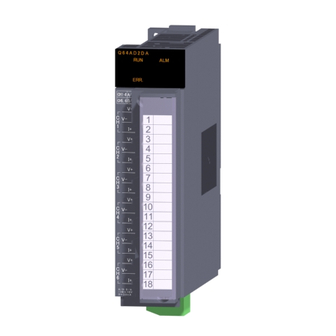
PREPARATORY PROCEDURES AND SETTING Part Names The following explains the part names of the Q64AD2DA. View A Module front surface side Base unit side View A Figure 7.2 Module appearance 7.3 Part Names... - Page 121 : Normal operation RUN LED : 5V power supply is shut off, watchdog timer error occurred, or online module change is enabled. Indicates the error and status of the Q64AD2DA. : Error Flashing : Switch setting error ERR. LED Other than 0 is set to the switch 5 of the intelligent function module.
-
Page 122: Wiring
The following explains the wiring precautions and module wiring examples. 7.4.1 Wiring precautions To achieve a reliable system and fully utilize the functionality of the Q64AD2DA, external wiring resistant to noise is required. This section provides wiring precautions. (1) Use separate cables for the AC control circuit and the external input signals of the Q64AD2DA to avoid the influence of the AC side surges and inductions. - Page 123 PREPARATORY PROCEDURES AND SETTING (5) The following actions are required for the module to comply with the EMC and Low Voltage Directives. (a) Always use a shielded twisted pair cable and ground it from the control panel through the AD75CK cable clamp (manufactured by Mitsubishi). In a control panel 20 to 30cm AD75CK...
- Page 124 PREPARATORY PROCEDURES AND SETTING (b) Install a ferrite core to an external power supply connection cable with keeping it 4cm away from the module. Ferrite core: ZCAT3035-1330 (manufactured by TDK Corporation.) External power supply connector External power supply connection cable Ferritie core External power supply 24VDC...
-
Page 125: External Wiring
Figure 7.5 External wiring example * 1 Use shielded twisted pair cables. * 2 The input resistance of the Q64AD2DA is shown. * 3 For current input, always connect the V+ terminal and I+ terminal. * 4 If noise or a ripple is generated in the external wiring, connect a capacitor of 0.1 to 0.47 F25V between the V+ terminal and COM terminal. -
Page 126: Wiring Of External Power Supply Connector
PREPARATORY PROCEDURES AND SETTING 7.4.3 Wiring of external power supply connector The Q64AD2DA requires a power supply (24VDC 15%) to run an analog circuit. Install an external power supply connector with referring to (2) in this section and (3) in this section. - Page 127 PREPARATORY PROCEDURES AND SETTING (2) Wiring method 1) Insert a cable to the terminal of external power supply connector. Check the terminal layout before wiring. Next, tighten the external power supply connector screw to secure the cable. Bottom surface of a module External power supply connector (accessory) Figure 7.7 Module bottom...
- Page 128 PREPARATORY PROCEDURES AND SETTING 2) Insert the connector to the terminal until the connector clicks into place. Anterior surface of a module Insert the connector into the terminal until Bottom surface the connector clicks of a module into place. Figure 7.8 Module side (3) Wiring example The following figure shows a wiring example of shielded twisted pair cables (example of CH1 analog voltage input).
-
Page 129: Setting From Gx Developer
Select "16points". Start XY Input the start I/O number of the Q64AD2DA. * 1 The above dialog box shows an example when the Q64AD2DA is mounted on a slot 0. 7.5 Setting from GX Developer - 12 7.5.1 Intelligent function module detailed setting... - Page 130 PREPARATORY PROCEDURES AND SETTING 4) Clicking the Detailed setting button opens the "Intelligent function module detailed setting" dialog box. Configure the setting with referring to the following. Setting for a programmable controller CPU stop error Figure 7.11 "Intelligent function module detailed setting" dialog box Table 7.7 Setting item in the "Intelligent function module detailed setting"...
-
Page 131: Intelligent Function Module Switch Setting
PREPARATORY PROCEDURES AND SETTING 7.5.2 Intelligent function module switch setting Configure input range setting, output range setting, analog output HOLD/CLEAR function setting, and resolution mode setting in this setting. The intelligent function module switch setting has switches 1 to 5 and is configured with 16-bit data. - Page 132 PREPARATORY PROCEDURES AND SETTING Switch setting 2) Clicking the button opens the "Switch setting for I/O and intelligent function module" dialog box. Configure the setting with referring to Table 7.8. Select HEX. Figure 7.13 "Switch setting for I/O and intelligent function module" dialog box Table 7.8 Intelligent function module switch setting Reference Switch...
-
Page 133: Offset/Gain Correction
PREPARATORY PROCEDURES AND SETTING Offset/Gain Correction The offset/gain can be corrected using the scaling function and shift function. The offset/gain correction examples are shown on the following pages. 7.6 Offset/Gain Correction - 16... - Page 134 PREPARATORY PROCEDURES AND SETTING (1) A/D conversion Example) When executing offset/gain correction under the following condition Analog input Analog input Scaling value Scaling value value value A/D conversion A/D conversion example before example after correction correction 20mA +4008 20mA +4000 conversion [Setting range: 0 to 20mA] Offset/gain correction...
- Page 135 PREPARATORY PROCEDURES AND SETTING POINT (1) When offset/gain are corrected using the scaling function and shift function, resolution may be reduced. In the example of Figure 7.14, the resolution is reduced at 0.125%. (2) When offset/gain are corrected using the scaling function and shift function, the functions cannot be used for other applications.
- Page 136 PREPARATORY PROCEDURES AND SETTING (2) D/A conversion Example: When executing offset/gain correction under the following condition Digital input Analog output Digital input Analog output value value value value D/A conversion D/A conversion 0.2mA example before example after 0.0mA correction correction 4000 20.3mA 20.0mA...
- Page 137 PREPARATORY PROCEDURES AND SETTING POINT (1) When offset/gain are corrected using the scaling function and shift function, resolution may be reduced. In the example of Figure 7.15, the resolution is reduced at 0.5%. (2) When offset/gain are corrected using the scaling function and shift function, the functions cannot be used for other applications.
-
Page 138: Chapter8 Utility Package (Gx Configurator-Ad/Gx Configurator-Da)
(1) Buffer memory of the Q64AD2DA to be auto-refreshed is set. Auto refresh setting (2) Buffer memory of the Q64AD2DA with the auto refresh setting is automatically read and written Section 8.5 to the specified device when the END instruction for the CPU module is executed. -
Page 139: Installing And Uninstalling The Utility Package
UTILITY PACKAGE (GX Configurator-AD/GX Configurator-DA) Installing and Uninstalling the Utility Package For how to install or uninstall the utility package, refer to "Method of installing the MELSOFT Series" included in the utility package. 8.2.1 Precautions for use This section provides precautions for using GX Configurator-AD and GX Configurator- * 1 Using either of the utilities can check the parameter settings of intelligent function module, setting status, and operating status of A/D and D/A conversions. - Page 140 GX Configurator-DA are as shown below. Table 8.3 The number of parameters that can be set for one module Module Initial setting Auto refresh setting GX Configurator-AD Q64AD2DA 8 (Fixed) 61 (Max.) GX Configurator-DA 8.2 Installing and Uninstalling the Utility Package 8.2.1 Precautions for use...
- Page 141 UTILITY PACKAGE (GX Configurator-AD/GX Configurator-DA) Example) Counting the number of set parameters in the auto refresh setting This one row is counted as one setting. Blank rows are not counted. Count up all the setting items on this window, and add the total to the number of settings for other intelligent function modules to get a grand total.
-
Page 142: Operating Environment
UTILITY PACKAGE (GX Configurator-AD/GX Configurator-DA) 8.2.2 Operating environment This section explains the operating environment of the personal computer that runs GX Configurator-AD and GX Configurator-DA. Table 8.4 Operating environment Item Description Installation (add-in) location GX Developer Version 4 (English version) or later Personal computer Windows -based personal computer... - Page 143 UTILITY PACKAGE (GX Configurator-AD/GX Configurator-DA) Table 8.5 Operating system and performance required for personal computer Performance required for personal computer Operating system Memory 32MB or more Windows Pentium 133MHz or more 32MB or more Windows Pentium 133MHz or more 32MB or more Windows Pentium 150MHz or more...
-
Page 144: Operating The Utility Package
UTILITY PACKAGE (GX Configurator-AD/GX Configurator-DA) Operating the Utility Package 8.3.1 Common operations (1) Control keys The following table shows control keys that can be used for utility operation and their applications. Table 8.6 Control keys that can be used Application Cancels a newly input value in a cell or exits the screen. - Page 145 UTILITY PACKAGE (GX Configurator-AD/GX Configurator-DA) (b) Text file A text file is created by clicking the Make text file button in the Initial setting window, Auto refresh setting window, and Monitor/Test window. The file can be utilized to create user documents. Figure 8.4 shows when GX Configurator-AD is used.
-
Page 146: Operation Overview
UTILITY PACKAGE (GX Configurator-AD/GX Configurator-DA) 8.3.2 Operation overview Figure 8.5 shows operations using the GX Configurator-AD window. The same operations apply to GX Configurator-DA. Window for selecting a target intelligent GX Developer window function module [Tools] - [Intelligent function module] - [Start] Section 8.3.3. - Page 147 UTILITY PACKAGE (GX Configurator-AD/GX Configurator-DA) FB Support Parameter tab [Online] - [Monitor/Test] - FB conversion Select monitor/test module dialog box FB conversion dialog box Section 8.7. Refer to Select a module to be monitored/tested. Monitor/Test window Section 8.6. Refer to Figure 8.5 Operation overview (continued) 8.3 Operating the Utility Package - 10...
-
Page 148: Starting Intelligent Function Module Utility
UTILITY PACKAGE (GX Configurator-AD/GX Configurator-DA) 8.3.3 Starting Intelligent function module utility [Operating procedure] Start Intelligent function module utility from GX Developer. Select [Tools] [Intelligent function utility] [Start]. [Setting window] The following shows a window when the "FB Support Parameter" tab is activated. Figure 8.6 Window for selecting a target intelligent function module [Description] (1) Display of other screens... - Page 149 UTILITY PACKAGE (GX Configurator-AD/GX Configurator-DA) When the "FB Support Parameter" tab is activated (d) Display of the FB conversion dialog box FB conversion "FB Support Parameter" tab Click the button. For details, refer to Section 8.7. POINT The "FB Support Parameter" tab opens when a project being edited is a label project.
- Page 150 • Select [Online] [Transfer setup] in GX Developer and set the target CPU module. • When mounting the Q64AD2DA on a remote I/O station, use "Read from PLC" and "Write to PLC" of GX Developer. (3) Checking required utility While the start I/O number is displayed in the Intelligent function module utility window, "...
-
Page 151: Initial Setting
UTILITY PACKAGE (GX Configurator-AD/GX Configurator-DA) Initial Setting [Purpose] Configure initial setting to operate the Q64AD2DA for each channel. For the types of initial setting parameters, refer to Section 8.1. Setting parameters in the Initial setting window can omit parameter settings with sequence program. - Page 152 UTILITY PACKAGE (GX Configurator-AD/GX Configurator-DA) [Description] (1) Setting items Set A/D conversion, D/A conversion enable/disable, and averaging process method for each channel. (2) Command buttons Writes data displayed in the window to a file in text file Make test file format.
-
Page 153: Auto Refresh Setting
UTILITY PACKAGE (GX Configurator-AD/GX Configurator-DA) Auto Refresh Setting [Purpose] Set buffer memory of the Q64AD2DA to be auto-refreshed. [Operating procedure] Input "Start I/O No." Select "Module type". Select "Module model name". Click the button. Auto refresh * 1 Input a start I/O number in hexadecimal. - Page 154 UTILITY PACKAGE (GX Configurator-AD/GX Configurator-DA) (2) Command buttons Writes data displayed in the window to a file in text file Make text file format. Saves settings and exits the window. End setup Cancels settings and exits the window. Cancel POINT The auto refresh setting is stored to an intelligent function module parameter.
-
Page 155: Monitor/Test
UTILITY PACKAGE (GX Configurator-AD/GX Configurator-DA) Monitor/Test 8.6.1 Monitor/Test window [Purpose] Start monitoring/testing the buffer memory and I/O signals, and "Operating condition setting" from this window. [Operating procedure] Select monitor/test module dialog box Input "Start I/O No." Select "Module Monitor/Test type". Select "Module model name". - Page 156 UTILITY PACKAGE (GX Configurator-AD/GX Configurator-DA) CH1 to CH4 Operating CH5, CH6 Operating condition setting condition setting Figure 8.9 "Monitor/Test" window (continued) - 19 8.6 Monitor/Test 8.6.1 Monitor/Test window...
- Page 157 (4) Input "10" as the average number of processing times and press the Enter key. At this point, the setting data have not been written to the Q64AD2DA. (5) Select the "Setting value" fields input in the operations (2) to (4) while pressing the key.
-
Page 158: Fb Conversion Of Initial Setting/Auto Refresh
UTILITY PACKAGE (GX Configurator-AD/GX Configurator-DA) FB Conversion of Initial Setting/Auto Refresh [Purpose] Convert automatically an intelligent function module parameter (initial setting/auto refresh setting) into an FB. [Operating procedure] Window for selecting a target intelligent function module Select the "FB Support FB conversion Parameter"... - Page 159 UTILITY PACKAGE (GX Configurator-AD/GX Configurator-DA) (2) Command button Converts a selected parameter (initial setting/auto refresh setting) Conversion into an FB. 8.7 FB Conversion of Initial Setting/Auto Refresh - 22...
-
Page 160: Usage Of Fb
UTILITY PACKAGE (GX Configurator-AD/GX Configurator-DA) Usage of FB This section explains procedures for using an FB with GX Developer. For details, refer to the "GX Developer Version 8 Operating Manual (Function Block)". 8.8.1 Overview The following shows procedures for creating an FB. 1) Set an intelligent function module parameter (initial setting/auto refresh setting). - Page 161 UTILITY PACKAGE (GX Configurator-AD/GX Configurator-DA) POINT The initial setting/auto refresh setting of the intelligent function module can be configured by either of the following methods. (1) Set an intelligent function module parameter (initial setting/auto refresh setting) and write it to the CPU module. (2) Create an FB of the intelligent function module parameter (initial setting/auto refresh setting) and paste it to the sequence program.
-
Page 162: Pasting An Fb To A Sequence Program
UTILITY PACKAGE (GX Configurator-AD/GX Configurator-DA) 8.8.2 Pasting an FB to a sequence program [Purpose] Paste an FB to use it in a sequence program. [Operating procedure] Switch the "Project" tab to the "FB" tab in GX Developer, and drag and drop an FB on the sequence program. -
Page 163: Converting (Compiling) A Sequence Program
UTILITY PACKAGE (GX Configurator-AD/GX Configurator-DA) 8.8.3 Converting (compiling) a sequence program [Purpose] Convert (compile) a sequence program to which an FB was pasted so that the program can be executed. Figure 8.13 Conversion (compilation) [Operating procedure] Select [Convert] [Convert/Compile] of GX Developer. 8.8 Usage of FB - 26 8.8.3 Converting (compiling) a sequence program... -
Page 164: Chapter9 Programming
PROGRAMMING CHAPTER9 PROGRAMMING This chapter explains programs of the Q64AD2DA. When applying the programs introduced in this chapter to an actual system, fully verify that the system control has no problems. Create a program in which A/D conversion or D/A conversion is performed with following the procedures shown in Figure 9.1. -
Page 165: Programming Procedures
PROGRAMMING Programming Procedures Create a program in which A/D conversion or D/A conversion is performed with following the procedures shown below. Start programming (1) Initial setting program Set up the initial setting with a sequence program. (Refer to CHAPTER 6 and Section 9.2.3.) (Refer to Use the utility package? Initial setting for... - Page 166 PROGRAMMING (1) Overview of the program examples The following processing is separately explained in the program examples. (a) Initial setting program of the Q64AD2DA (b) A/D conversion program 1) CH1 to CH3 Reading of a scaling value 2) CH3 Processing when an input signal detects an error...
-
Page 167: Programming For Normal System Configuration
(1) System configuration QCPU QY10 (Y20 to Y2F) QX10 (X10 to X1F) Q64AD2DA (X/Y0 to X/YF) Figure 9.2 System configuration example (2) Conditions of the intelligent function module switch setting (a) A/D conversion Table 9.1 Conditions of the intelligent function module switch setting... - Page 168 PROGRAMMING (3) Programming conditions (a) Used channels A/D conversion: CH1 to CH3 D/A conversion: CH5 and CH6 (CH4 is not used in the program examples.) (b) Use the following A/D conversion methods for each channel. • CH1: Sampling processing • CH2: Count average (50 times) •...
-
Page 169: Before Program Creation
This section explains works required before program creation. (1) Wiring of external devices (Refer to Section 7.4.2.) Mount the Q64AD2DA on a base unit and wire external devices to the following channels. Table 9.3 Channels to which external devices are wired... - Page 170 PROGRAMMING (2) Intelligent function module switch setting (Refer to Section 7.5.2.) Based on the setting conditions given in Section 9.2 (2), configure the intelligent function module switch setting. (a) Switch settings 1) Switch 1: Input range setting (CH1 to CH4) <Switch 1>...
- Page 171 PROGRAMMING (b) Switch setting for function module Switch setting Click on button in the "I/O assignment" tab of the parameter setting dialog box of GX Developer to display the dialog box shown below, then set switches 1 to 5. Figure 9.9 Intelligent function module switch setting with GX Developer 9.2 Programming for Normal System Configuration 9.2.1 Before program creation...
-
Page 172: 9.2.2 Program Example Using The Utility Package
CH6 Initial digital input value Module ready Input signal error detection signal Error flag CH5 Output enable/disable flag Q64AD2DA (X/Y0 to X/YF) CH6 Output enable/disable flag Operating condition setting request Error clear request Device turned on by user to start reading... - Page 173 PROGRAMMING (2) Utility package operation (a) Initial setting (Refer to Section 8.4.) Set the items shaded in the table below to the initial settings of CH1 to CH3, CH5, and CH6. Setting for the items with "-" is not required when "Disable" has been set. (The default value, which will be displayed in the "Setting value"...
- Page 174 PROGRAMMING Table 9.6 List of initial setting items (D/A conversion area) Setting item Default D/A conversion enable/disable Disable Enable Enable setting D/A conversion scaling enable/ Disable Disable Enable disable setting D/A conversion scaling lower 1000 limit value Setting is not required since "Disable"...
- Page 175 PROGRAMMING 2) Clicking the Initial setting button of each channel opens a window as shown below. Set the initial setting items listed in Table 9.5 and Table 9.6 in the window. The following is the example windows of "CH1 Initial setting" and "CH5 Initial setting".
- Page 176 PROGRAMMING For operations of the utility package, refer to Section 8.5. For setting of "PLC side Device" in the "Auto refresh setting" window, refer to the assignment shown in (1) in this section Device list. Figure 9.13 "Auto refresh setting" screen (c) Writing intelligent function module parameters (Refer to Section 8.3.3.) Write the intelligent function module parameters to the CPU module.
- Page 177 PROGRAMMING (3) Program example 1. Reading scaling values Reads scaling values of CH1 to CH3 2. Detecting an input signal error and processing the error detection Processing CH3 input signal error detection Resets Input signal error detection signal (X7) 3. Setting default digital input values 4.
-
Page 178: Program Example Without Using The Utility Package
Module ready Input signal error detection signal Operating condition setting completion flag Error flag Q64AD2DA (X/Y0 to X/YF) CH5 Output enable/disable flag CH6 Output enable/disable flag Operating condition setting request Error clear request Device turned on by user to start reading... - Page 179 PROGRAMMING (2) List of used buffer memory addresses Table 9.8 List of used buffer memory addresses Setting Address Description Remarks value Un\G0 CH1 A/D conversion enable/disable setting Enable CH1. Measured CH1 Scaling value Un\G102 CH1 Scaling value is stored. Completion status of the first A/D Un\G113 CH1 A/D conversion completed flag conversion of CH1 is stored.
- Page 180 PROGRAMMING (3) Program example Programming the Q64AD2DA initial setting Enables A/D conversion of CH1 and Sets average processing of CH2 Sets A/D conversion scaling function of CH2 Enables A/D conversion of CH3 Sets average processing of CH3 Defaults input signal error detection...
- Page 181 PROGRAMMING Detecting an input signal error and processing the error detection Processing CH3 input signal error detection Resets Input signal error detection signal (X7) Setting default digital input values Writing digital input values Sets digital input values of CH5 and Setting enabling analog output Enables analog output of CH5 and Displaying error codes and resetting...
-
Page 182: Programming For Remote I/O Network
(Station No.0) (Station No.1) QJ71LP21-25 (X/Y0 to XY1F) QX10 (X20 to X2F) QY10 (Y30 to Y3F) Q64AD2DA (X/Y1000 to X/Y100F) QJ72LP25-25 Network No.1 Figure 9.16 System configuration example (2) Conditions of the intelligent function module switch setting (a) A/D conversion Table 9.9 Conditions of the intelligent function module switch setting... - Page 183 PROGRAMMING (3) Programming conditions (a) Used channels A/D conversion: CH1 to CH3 D/A conversion: CH5 and CH6 (CH4 is not used in the program examples.) (b) Use the following A/D conversion methods for each channel. • CH1: Sampling processing • CH2: Count average (50 times) •...
-
Page 184: Before Program Creation
Before program creation This section explains works required before program creation. (1) Wiring of external devices Mount the Q64AD2DA on a base unit and wire external devices to CH1 to CH3, CH5, and CH6. For wiring method, refer to Section 9.2.1 (1). -
Page 185: 9.3.2 Program Example Using The Utility Package
Module ready X1007 Input signal error detection signal X100F Error flag Y1005 CH5 Output enable/disable flag Q64AD2DA (X/Y1000 to X/Y100F) Y1006 CH6 Output enable/disable flag Y1009 Operating condition setting request Y100F Error clear request 9.3 Programming for Remote I/O Network - 22 9.3.2 Program example using the utility package... - Page 186 PROGRAMMING (2) GX Developer operation (setting of the network parameter) • Network type : MNET/H (Remote master) • Starting I/O No. : 0000 • Network No. • Total stations • Mode : On line • Network range assignment : Figure 9.18 "Network range assignment" screen •...
- Page 187 PROGRAMMING (3) Utility package operation Operate on the remote I/O station side. (a) Initial setting (For operations of the utility package, refer to Section 8.4.) Configure the initial settings of CH1 to CH3, CH5, and CH6. For details, refer to Section 9.2.2 (2). (b) Auto refresh setting (For operations of the utility package, refer to Section 8.5.) Set devices storing the following buffer memory data to each item.
- Page 188 PROGRAMMING Figure 9.20 "Auto refresh setting" window (c) Writing intelligent function module parameters (Refer to Section 8.3.3.) Write the intelligent function module parameters to the remote I/O station. Configure the setting in the window for selecting a target intelligent function module.
- Page 189 PROGRAMMING (4) Program example 1. Reading scaling values Reads scaling values of CH1 to CH3 2. Detecting an input signal error and processing the error detection Processing CH3 input signal error detection Resets Input signal error detection signal (X1007) 3. Setting default digital input values 4.
- Page 190 Module ready X1007 Input signal error detection signal Operating condition setting completion X1009 flag X100F Error flag Q64AD2DA (X/Y1000 to X/Y100F) Y1005 CH5 Output enable/disable flag Y1006 CH6 Output enable/disable flag Y1009 Operating condition setting request Y100F Error clear request...
- Page 191 CH2 Initial setting #2 transfer check flag M222 CH2 Initial setting #2 completion flag Device for write operation of the initial settings for the Q64AD2DA M230, M231 CH3 Initial setting #1 transfer check flag M232 CH3 Initial setting #1 completion flag...
- Page 192 (2) List of used buffer memory addresses The Z(P).REMFR or Z(P).REMTO instruction is used to access the buffer memory of the Q64AD2DA. Check the access device in the "Address (device)" column in Table 9.13. Table 9.13 List of used buffer memory addresses...
- Page 193 PROGRAMMING Table 9.13 List of used buffer memory addresses Setting Address (device) Description Remarks value Measured CH5 Digital input Un\G802 (D31) CH5 Digital input value value is stored. CH6 D/A conversion enable/disable Un\G1000 (D1050) Enable CH6. setting Measured CH6 Digital input Un\G1002 (D32) CH6 Digital input value value is stored.
- Page 194 PROGRAMMING (4) Program example 1. Checking remote I/O station operation status Checks master station baton pass status Checks master station data link status Checks remote I/O station baton pass status Checks remote I/O station data link status Checks remote I/O station parameter communication status Checks master module...
- Page 195 PROGRAMMING 2.2 Initial setting of CH2 #1 (A/D conversion enable setting, count average setting) Enables A/D conversion of CH2 Sets averaging processing of CH2 2.3 Initial setting of CH2 #2 (scaling setting) Sets A/D conversion scaling function of CH2 2.4 Initial setting of CH3 #1 (A/D conversion enable setting, moving average setting) Enables A/D conversion of CH3 Sets averaging...
- Page 196 PROGRAMMING 2.8 Initial setting of CH6 #2 (scaling setting) Sets D/A conversion scaling function of CH6 2.9 Turning on Y1009 after all initial setting data (2.1 to 2.8) are written normally. Turns on Operating condition setting request (Y1009) Turns off Operating condition setting request (Y1009) 3.
- Page 197 PROGRAMMING 4. Detecting an input signal error and processing the error detection Processing CH3 input signal error detection Resets Input signal error detection signal (X1007) 5. Setting default digital input values 6. Writing digital input values Sets digital input values of CH5 and CH6 7.
-
Page 198: Chapter10 Online Module Change
ONLINE MODULE CHANGE CHAPTER10 ONLINE MODULE CHANGE When changing a module online, carefully read the "Online module change" section in the QCPU User's Manual (Hardware Design, Maintenance and Inspection). This chapter explains the specifications of the online module change. [Precautions] This chapter explains using device numbers (X/Y) and buffer memory addresses for CH1 and CH5. -
Page 199: Execution Condition Of Online Module Change
Remark The online module change is supported by the Q64AD2DA of the first product to the function version C. 10.1 Execution Condition of Online Module Change... -
Page 200: Operations During Online Module Change
ONLINE MODULE CHANGE 10.2 Operations During Online Module Change The following table shows operations during online module change. Table 10.1 Operations during online module change CPU operation : Performed : Not performed GX Configurator (Operation of intelligent function FROM/TO (User operation) Dedicated Device Initial... -
Page 201: Procedures Of Online Module Change
ONLINE MODULE CHANGE 10.3 Procedures of Online Module Change This section explains the procedures of online module change when an initial setting of GX Configurator-AD or GX Configurator-DA is configured and when the initial setting is not configured. Table 10.2 Procedures of online module change Initial setting Reference GX Configurator-AD or GX Configurator-DA... - Page 202 ONLINE MODULE CHANGE (2) Removing a module (a) After choosing "Online module change" Mode in the dialog box opened by selecting [Diagnostics] [Online module change] of GX Developer, double-click a module to be changed online to display the "Online module change" dialog box. Figure 10.2 "System Monitor"...
- Page 203 ONLINE MODULE CHANGE (c) After checking that the RUN LED of the module turned off, remove the terminal block, external power supply connector, and then the module. POINT Always remove the module. If mounting status is checked without the module removed, the module will not properly start and the RUN LED will not turn on.
- Page 204 ONLINE MODULE CHANGE (b) Click the button to suspend the online module change mode. Figure 10.7 Dialog box informing the suspension of online module change mode (c) Click the Close button to close the "System Monitor" dialog box. Figure 10.8 "System Monitor" dialog box 10.3 Procedures of Online Module Change 10.3.1 When the initial setting has been configured with GX Configurator-AD or GX Configurator-DA...
- Page 205 ONLINE MODULE CHANGE (d) Set CH1 A/D conversion enable/disable setting (Un\G0) or CH5 D/A conversion enable/disable setting (Un\G800) to "Enable" (0) and turn off and then on Operating condition setting request (Y9). 1) A/D conversion (CH1 to CH4) Monitor CH1 Digital output value (Un\G100) to check if A/D conversion is properly performed.
- Page 206 ONLINE MODULE CHANGE (b) Dialog box informing the completion of online module change appears. Figure 10.11 Dialog box informing the completion of online module change 10.3 Procedures of Online Module Change 10.3.1 When the initial setting has been configured with GX Configurator-AD or GX Configurator-DA...
-
Page 207: When The Initial Setting Has Been Configured With Sequence Program
ONLINE MODULE CHANGE 10.3.2 When the initial setting has been configured with sequence program (1) Disabling conversion (a) Take the following steps to disable the conversion: 1) Set CH1 A/D conversion enable/disable (Un\G0) and CH5 D/A conversion enable/disable (Un\G800) to Disable (1). 2) Turn Operating condition setting request (Y9) from off to on to stop the conversion. - Page 208 ONLINE MODULE CHANGE (2) Removing a module (a) After choosing "Online module change" Mode in the dialog box opened by selecting [Diagnostics] [Online module change] of GX Developer, double-click a module to be changed online to display the "Online module change" dialog box. Figure 10.13 "System Monitor"...
- Page 209 ONLINE MODULE CHANGE (c) After checking that the RUN LED of the module turned off, remove the terminal block, external power supply connector, and then the module. POINT Always remove the module. If mounting status is checked without the module being removed, the module will not properly start and the RUN LED will not turn (3) Mounting a new module (a) Mount a new module on the same slot, and install a terminal block and external...
- Page 210 ONLINE MODULE CHANGE (4) Operation check (a) To check operations, click the Cancel button and see if the restart of control is canceled. Figure 10.17 "Online module change" (restart of module control) dialog box (b) Click the button to suspend the online module change mode. Figure 10.18 Dialog box informing the suspension of online module change mode Close (c) Click the...
- Page 211 1) Normal system configuration The sequence program should perform initialization on the leading edge of Module ready (X0) of the Q64AD2DA. When control resumption is executed, Module ready (X0) turns on and initialization is performed. (If the sequence program performs initialization only for one scan after RUN, initialization is not performed.)
- Page 212 ONLINE MODULE CHANGE (5) Restarting control (a) After choosing [Diagnostics] [Online module change] in GX Developer to display the "Online module change" screen again, click the Execution button to resume controls such as I/O, FROM/TO instruction executions, and automatic refresh for the module. Figure 10.20 "Online module change"...
-
Page 213: Chapter11 Troubleshooting
TROUBLESHOOTING CHAPTER11 TROUBLESHOOTING This chapter describes the errors which may occur during the use of the Q64AD2DA and troubleshooting. The device numbers (X or Y) and buffer memory addresses described in this chapter are used for the channel 1. (The device numbers and buffer memory addresses specified in D/A conversion are used for CH5.) -
Page 214: Troubleshooting
TROUBLESHOOTING (3) Error code list Errors are classified into two levels: moderate (module error) and minor (module warning). When a moderate error occurs, conversion processing is not performed. When a minor error occurs, conversion processing is performed with the settings that the system operated normally last time. - Page 215 TROUBLESHOOTING Table 11.3 Errors related to channels (continued) Error code Corresponding Error Reference Description Corrective action channel level section (decimal) A value other than the range from 4 to 20000 times is set to CH1 Reset the averaging count setting to within 4 to Section 6.4 Averaging process (time / number 20000 times.
- Page 216 TROUBLESHOOTING Table 11.3 Errors related to channels (continued) Error code Corresponding Error Reference Description Corrective action channel level section (decimal) • A value less than -32000 is set to CH1 A/D conversion scaling lower limit value (Un\G11) or CH5 D/A conversion scaling lower limit Section 6.6 value (Un\G811).
-
Page 217: When "Run" Led Turns Off
TROUBLESHOOTING 11.2 Troubleshooting 11.2.1 When "RUN" LED turns off Table 11.4 When "RUN" LED turns off Reference Check item Corrective action section Check that the supply voltage of the power supply module Section Is power supplied? is within the rated range. Calculate the current consumption of the CPU, I/O, intelligent function and other modules mounted on the Is the capacity of the power supply module sufficient? -
Page 218: When Digital Output Values Cannot Be Read
TROUBLESHOOTING 11.2.4 When digital output values cannot be read Table 11.8 When digital output values cannot be read Reference Check item Corrective action section Section Check that External power off flag (X6) is set to on and 5.2.1 Is 24VDC external supply power being supplied? supply 24VDC external supply power to the external Section power supply connector terminal. -
Page 219: 11.2.5 When A/D Conversion Completed Flag Does Not Turn On During Use In Normal Mode
TROUBLESHOOTING 11.2.5 When A/D conversion completed flag does not turn on during use in normal mode Table 11.9 When A/D conversion completed flag does not turn on during use in normal mode Reference Check item Corrective action section Section Is an input signal error being generated? Check CH1 Input signal error detection flag (Un\G114). -
Page 220: When External Power Off Flag (X6) Turns On
(2) Supply 24VDC within the range of the performance Section specified range? specifications. 7.4.2 The possible cause is a failure of the Q64AD2DA. Please The case other than the above consult your local Mitsubishi representative. 11.2 Troubleshooting 11.2.7 When External power off flag (X6) turns on... -
Page 221: Checking The Q64Ad2Da Status
* 1 The latest error code among the error codes in the list shown in Section 11.1 (3) and Section 11.1 (3) is displayed in the Present Error field. * 2 The error history can be checked in the buffer memory. (Refer to Section 11.1.) 11.2 Troubleshooting 11.2.8 Checking the Q64AD2DA status... - Page 222 Switch 2: Output range setting (CH5 and CH6) Switch 3: Analog output HOLD/CLEAR function setting (CH5 and Section CH6) 7.5.2 Switch 4: Mode setting Switch 5: - Figure 11.2 H/W Information dialog box - 10 11.2 Troubleshooting 11.2.8 Checking the Q64AD2DA status...
- Page 223 Un\G1191 0000 Un\G1194 Error codes Un\G1790 unrelated to Un\G1791 channels. 0000 Un\G1960 Un\G1794 Error history 16 Un\G1961 0000 Un\G1964 Figure 11.3 Buffer memory in the case of more than one error 11.2 Troubleshooting - 11 11.2.8 Checking the Q64AD2DA status...
- Page 224 Up to last eight error history can be checked in the Module's Detailed Information dialog box. Newer error codes are displayed in the bottom of the error history field. Figure 11.4 System monitor error history in the case of more than one error - 12 11.2 Troubleshooting 11.2.8 Checking the Q64AD2DA status...
-
Page 225: Appendix 1 External Dimensions
APPENDIX APPENDIX Appendix 1 External Dimensions 27.4 Unit: mm Appendix 1 External Dimensions... - Page 226 APPENDIX Memo Appendix 1 External Dimensions...
- Page 227 INDEX FB conversion............8-21 Function version ............ 2-5 ALM LED ............... 7-4 Analog conversion enable/disable setting ... 4-33 Analog output HOLD/CLEAR function....4-25 Analog output HOLD/CLEAR function setting ..7-15 Gain value............3-4,3-9 Analog output test during a CPU module STOP ................
- Page 228 Minimum digital output value (Un\G106, Un\G1721) ................6-22 Minimum scaling value (Un\G110, Un\G1741) ..6-23 Mode setting ............7-15 Module ready (X0) ..........5-2 Monitor/Test............8-18 Moving average ............. 4-5 Offset value ............. 3-4,3-9 Offset/gain correction .......... 7-16 Oldest pointer (Un\G120) ........6-26 Online module change.........
- Page 229 Warranty Please confirm the following product warranty details before using this product. 1. Gratis Warranty Term and Gratis Warranty Range If any faults or defects (hereinafter "Failure") found to be the responsibility of Mitsubishi occurs during use of the product within the gratis warranty term, the product shall be repaired at no cost via the sales representative or Mitsubishi Service Company.
- Page 230 Microsoft and Windows are either registered trademarks or trademarks of Microsoft Corporation in the United States and/or other countries. Intel, Pentium, and Celeron are either registered trademarks or trademarks of Intel Corporation in the United States and/or other countries. Ethernet is a registered trademark of Fuji Xerox Corporation in Japan. The company names, system names and product names mentioned in this manual are either registered trademarks or trademarks of their respective companies.
- Page 232 SH(NA)-080793ENG-E(1611)MEE MODEL: Q64AD2DA-U-SY-E MODEL CODE: 13JZ25 HEAD OFFICE : TOKYO BUILDING, 2-7-3 MARUNOUCHI, CHIYODA-KU, TOKYO 100-8310, JAPAN NAGOYA WORKS : 1-14 , YADA-MINAMI 5-CHOME , HIGASHI-KU, NAGOYA , JAPAN When exported from Japan, this manual does not require application to the Ministry of Economy, Trade and Industry for service transaction permission.