Table of Contents
Advertisement
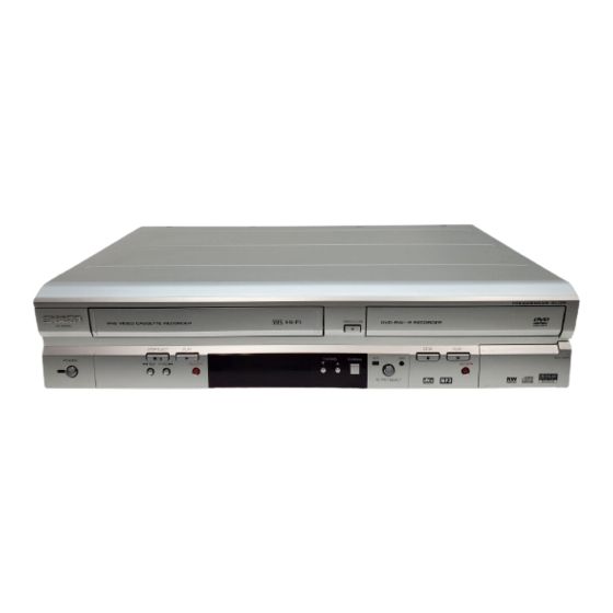
VCR/DVD RECORDER COMBINATION
The region number for
1
this unit is 1.
1. SPECIFICATIONS ................................................................................................................................................ 1-1-1
2. LASER BEAM SAFETY PRECAUTIONS ............................................................................................................. 1-2-1
3. IMPORTANT SAFEGUARDS AND PRECAUTIONS ............................................................................................ 1-3-1
4. STANDARD NOTES FOR SERVICING ................................................................................................................ 1-4-1
5. PREPARATION FOR SERVICING ....................................................................................................................... 1-5-1
6. OPERATING CONTROLS AND FUNCTIONS ...................................................................................................... 1-6-1
7. CABINET DISASSEMBLY INSTRUCTIONS ........................................................................................................ 1-7-1
8. HOW TO INITIALIZE THE DVD RECORDER & VCR .......................................................................................... 1-8-1
9. ELECTRICAL ADJUSTMENT INSTRUCTIONS ................................................................................................... 1-9-1
10. FIRMWARE RENEWAL MODE (FIRMWARE VERSION UP) ............................................................................ 1-10-1
11. TROUBLESHOOTING ........................................................................................................................................ 1-11-1
12. FUNCTION INDICATOR SYMBOLS ................................................................................................................... 1-12-1
13. BLOCK DIAGRAMS ............................................................................................................................................ 1-13-1
14. SCHEMATIC DIAGRAMS/ CBA'S AND TEST POINTS ..................................................................................... 1-14-1
15. WAVEFORMS & VOLTAGE CHART .................................................................................................................. 1-15-1
16. WIRING DIAGRAM ............................................................................................................................................. 1-16-1
17. SYSTEM CONTROL TIMING CHARTS .............................................................................................................. 1-17-1
18. IC PIN FUNCTION DESCRIPTIONS .................................................................................................................. 1-18-1
19. LEAD IDENTIFICATIONS ................................................................................................................................... 1-19-1
20. EXPLODED VIEWS ............................................................................................................................................ 1-20-1
21. MECHANICAL PARTS LIST ............................................................................................................................... 1-21-1
22. ELECTRICAL PARTS LIST ................................................................................................................................ 1-22-1
1. STANDARD MAINTENANCE ............................................................................................................................... 2-1-1
2. SERVICE FIXTURE AND TOOLS ........................................................................................................................ 2-2-1
3. MECHANICAL ALIGNMENT PROCEDURES ...................................................................................................... 2-3-1
4. DISASSEMBLY / ASSEMBLY PROCEDURES OF DECK MECHANISM ............................................................ 2-4-1
5. ALIGNMENT PROCEDURES OF MECHANISM .................................................................................................. 2-5-1
6. DECK EXPLODED VIEWS ................................................................................................................................... 2-6-1
7. DECK PARTS LIST ............................................................................................................................................... 2-7-1
SHARP CORPORATION
SERVICE MANUAL
MODEL
CONTENTS
1
DV-RW550U
In the interests of user-safety (Required by safety
regulations in some countries) the set should be
restored to its original condition and only parts
identical to those specified be used.
This document has been published to be used for
after sales service only.
The contents are subject to change without notice.
DV-RW550U
S35F2DV-RW550
Advertisement
Table of Contents

Related Manuals for Sharp DV-RW550U


Summary of Contents for Sharp DV-RW550U
-
Page 1: Table Of Contents
DV-RW550U SERVICE MANUAL S35F2DV-RW550 VCR/DVD RECORDER COMBINATION MODEL DV-RW550U The region number for this unit is 1. In the interests of user-safety (Required by safety regulations in some countries) the set should be restored to its original condition and only parts identical to those specified be used. -
Page 2: Main Section
MAIN SECTION VCR/DVD RECORDER COMBINATION DV-RW550U TABLE OF CONTENTS 1. SPECIFICATIONS ..................1-1-1 2. LASER BEAM SAFETY PRECAUTIONS ............1-2-1 3. IMPORTANT SAFEGUARDS AND PRECAUTIONS ........1-3-1 4. STANDARD NOTES FOR SERVICING ............1-4-1 5. PREPARATION FOR SERVICING ..............1-5-1 6. -
Page 3: Specifications
SPECIFICATIONS < VCR Section > Description Unit Minimum Nominal Maximum Remark 1. Video 1-1. Video Output ( PB ) Vp-p SP Mode 1-2. Video Output ( R/P ) Vp-p SP Mode, 1-3. Video S/N Y ( R/P ) W/O Burst 1-4. - Page 4 < DVD Section > ITEM CONDITIONS UNIT NOMINAL LIMIT 1. VIDEO 1-1. Video Output 75 ohm load Vp-p 1-2. S-Video Output Y (Luminance) 75 ohm load Vp-p C (Chrominance) 75 ohm load Vp-p 0.286 1-3. Component Output Y (Luminance) 75 ohm load Vp-p Cb (Chrominance) 75 ohm load...
-
Page 5: Laser Beam Safety Precautions
LASER BEAM SAFETY PRECAUTIONS This DVD player uses a pickup that emits a laser beam. Do not look directly at the laser beam coming from the pickup or allow it to strike against your skin. The laser beam is emitted from the location shown in the figure. When checking the laser diode, be sure to keep your eyes at least 30cm away from the pickup lens when the diode is turned on. -
Page 6: Important Safeguards And Precautions
IMPORTANT SAFEGUARDS AND PRECAUTIONS 1. IMPORTANT SERVICE NOTES BEFORE RETURNING THE DVD VIDEO PLAYER Reverse the AC plug on the set and repeat AC voltage measurements for each exposed part. Any reading of Before returning the DVD video player to the user, 0.45V rms (this corresponds to 0.3mA rms AC.) or more is excessive and indicates a potential shock perform the following safety checks. - Page 7 WARNING :TO REDUCE THE RISK OF FIRE OR ELECTRIC SHOCK, DO NOT EXPOSE THIS APPLIANCE TO WET LOCATIONS. CAUTION CAUTION RISK OF ELECTRIC SHOCK DO NOT OPEN This symbol mark means following. For continued protection against fire CAUTION: TO REDUCE THE RISK OF ELECTRIC hazard, replace only with same type SHOCK.
-
Page 8: Standard Notes For Servicing
STANDARD NOTES FOR SERVICING NOTE: CBA AND PWB MEANS PRINTED WIRING Using lead-free wire solder BOARD. When fixing the PWB soldered with the lead-free solder, Circuit Board Indications apply lead-free wire solder. Repairing with conventional lead wire solder may cause damage or accident due to a. - Page 9 Soldering Iron Fig. S-1-3 (2) Lift each lead of the flat pack-IC upward one by one, using a sharp pin or wire to which solder will not adhere (iron wire). When heating the pins, use a fine Fig. S-1-1 tip soldering iron or a hot air desoldering machine.
- Page 10 (4) Bottom of the flat pack-IC is fixed with glue to the 2. Installation CBA; when removing entire flat pack-IC, first apply (1) Using desoldering braid, remove the solder from the soldering iron to center of the flat pack-IC and heat foil of each pin of the flat pack-IC on the CBA so you up.
- Page 11 Instructions for Handling Semi-conductors Electrostatic breakdown of the semi-conductors may occur due to a potential difference caused by electrostatic charge during unpacking or repair work. 1. Ground for Human Body Be sure to wear a grounding band (1MΩ) that is properly grounded to remove any static electricity that may be charged on the body.
-
Page 12: Preparation For Servicing
PREPARATION FOR SERVICING How to Enter the Service Mode About Optical Sensors Caution: An optical sensor system is used for the Tape Start and End Sensors on this equipment. Carefully read and follow the instructions below. Otherwise the unit may operate erratically. -
Page 13: Operating Controls And Functions
OPERATING CONTROLS AND FUNCTIONS E9656IB 1-6-1... - Page 14 E9656IB 1-6-2...
- Page 15 E9656IB 1-6-3...
-
Page 16: Cabinet Disassembly Instructions
CABINET DISASSEMBLY INSTRUCTIONS NOTE: CBA AND PWB MEANS PRINTED WIRING REMOVAL BOARD. REMOVE/*UNHOOK/ LOC. PART Fig. UNLOCK/RELEASE/ Note 1. Disassembly Flowchart UNPLUG/DESOLDER This flowchart indicates the disassembly steps to gain Rear Panel 5(S-6), 3(S-7), (S-8), access to item(s) to be serviced. When reassembling, Unit *CN101, *CN102 follow the steps in reverse order. - Page 17 Reference Notes [5] Jack Bracket (S-4) CAUTION 1: Locking Tabs (L-1) and (L-2) are fragile. Be careful not to break them. 1-1. Release five Locking Tabs (L-1). 1-2. Release three Locking Tabs (L-2). 1-3. Disconnect Connector (CN1609), and remove the Front Assembly.
- Page 18 (S-14) (S-7) (S-13) (S-14) (S-8) (S-13) (S-6) (S-13) (S-14) (S-15) [8] Rear (S-7) Panel Unit (S-14) (S-16) (S-7) (S-12) [14] VCR (S-14) Chassis Unit CN102 CN101 [13] Bracket R Fig. D5 Fig. D7 [12] Rear Panel (S-11) (S-10) (S-11) [10] DC Fan Motor AC Cord Hook [9] Power...
- Page 19 Cylinder Assembly FE Head ACE Head Assembly SW512 LD-SW [15] Deck Assembly [16] Power SW CBA [17] Function [18] Main CBA [15] Deck Assembly (S-17) Cam Gear [18] Main Hole Lead Shaft with (S-18) blue Desolder stripe Hole LD-SW [18] Main CBA Desolder Lead with blue stripe...
- Page 20 (S-19) (S-19) [19] Deck Pedestal [20] Front Bracket R (S-20) Fig. D9 E9656DC 1-7-5...
- Page 21 3. How to Eject Manually < Method 1 > Note: When servicing, do not touch white resin part as shown below. When rotating the gear, be careful not to damage the gear. 1. Remove the Top Cover. 2. Rotate the gear in the direction of the arrow manually as shown below. View for A Do not touch! Rotate this gear in...
- Page 22 < Method 2 > 4. Release the other side of two Locking Tabs, and Note: When servicing, do not touch white resin part remove the Clamper Assembly. as shown below. 1. Remove the Top Cover, the Front Assembly and the DVD Mechanism & DVD Main CBA Assembly. Then, remove the DVD Mechanism Unit.
-
Page 23: How To Initialize The Dvd Recorder & Vcr
HOW TO INITIALIZE THE DVD RECORDER & VCR To put the program back at the factory-default, initialize the DVD recorder & VCR as the following procedure. < DVD Recorder Section > 1. Turn the DVD recorder on. 2. Confirm that no disc is loaded or that the disc tray is open. -
Page 24: Electrical Adjustment Instructions
ELECTRICAL ADJUSTMENT INSTRUCTIONS NOTE: CBA AND PWB MEANS PRINTED WIRING BOARD. Figure 1 EXT. Syncronize Trigger Point NOTES: 1. Electrical adjustments are required after replacing circuit components and certain mechanical parts. It is important to do these adjustments only after all 1.0H 0.5H repairs and replacements have been completed. -
Page 25: Firmware Renewal Mode (Firmware Version Up)
FIRMWARE RENEWAL MODE (FIRMWARE VERSION UP) NOTES: * Firmware Version differs depending on the a. This unit can not read data which is written with models, and this indication is one example. packet write software (ex. B's Clip). b. The file system should be set to Joliet or ISO9660 Firm Update Mode ver. - Page 26 5. After updating is finished, the tray opens automatically. Fig. f appears on the screen and Fig. g appears on the VFD. * Firmware Version differs depending on the models, and this indication is one example. Firm Update Mode ver. R2F3000S1E R2F3001S1E B/E Firmware Update End...
-
Page 27: Troubleshooting
TROUBLESHOOTING Table of Contents for the Troubleshooting Flow Charts Flow Chart Description Page The power cannot be turned on. 1-11-2 The fuse blows out. 1-11-2 When the output voltage fluctuates. 1-11-2 When buzz sound can be heard in the vicinity of power circuit. 1-11-2 -FL AL-30V is not outputted. -
Page 28: Power Supply Section
1. Power Supply Section FLOW CHART NO.1 The power cannot be turned on. See FLOW CHART No.2 <The fuse blows out.> Is the fuse normal? Is normal state restored when once unplugged Check for lead or short-circuiting of primary power cord is plugged again after several seconds. circuit component and service it if defective. - Page 29 FLOW CHART NO.6 P-ON+9V is not outputted. Check D012, D014, D017, C012, and their Is 12V voltage supplied to the collector of Q055? periphery, and service it if defective. Is 10V voltage supplied to the base of Q055? Is the "L" pulse inputted to the base of Q052? Replace Q055.
- Page 30 FLOW CHART NO.11 DVD-P-ON+5V is not outputted. Is 5V voltage supplied to the collector of Q101? Check D015, D016, C017, C019, L012 and their periphery, and service it if defective. Check Q101 and their periphery, and service it if defective. FLOW CHART NO.12 P-ON+2.5V is not outputted.
- Page 31 2. DVD Section FLOW CHART NO.1 The key operation is not functioning. Are the contact point and the installation state of Re-install some key switches correctly or the key switches normal? replace some key switches. Check the key switches and their periphery, and Is the control voltage normally inputted into service it if defective.
- Page 32 FLOW CHART NO.4 The disc tray cannot be opened and closed. Replace the DVD Mechanism & DVD Main CBA Assembly. FLOW CHART NO.5 [No Disc] indicated. Replace the DVD Mechanism & DVD Main CBA Assembly. FLOW CHART NO.6 Both functions of picture and sound do not operate normally. Replace the DVD Mechanism &...
- Page 33 Replace the DVD Mechanism & DVD Main CBA Are the video signals outputted to each pin of Assembly. CN201 on the MAIN CBA? CN201 7PIN VIDEO-Y(I/P) CN201 3PIN VIDEO-Cr/Pr CN201 5PIN VIDEO-Cb/Pb CN201 1PIN VIDEO-Y(I) CN201 9PIN VIDEO-C Check the line between each pin of CN201 and Are the video signals shown above inputted into each pin of IC1404 and IC1405 on the MAIN CBA, each pin of IC1404 and each pin of IC1405?
- Page 34 FLOW CHART NO.8 Picture does not appear normally. Set the disc on the disc tray, and playback. Replace the DVD Mechanism & DVD Main CBA Are the video signals outputted to each pin of Assembly. CN201 on the MAIN CBA? CN201 7PIN VIDEO-Y(I/P)
- Page 35 FLOW CHART NO.9 Audio E-E does not appear normally. No (Rear or Check the line between audio input terminal and each pin of IC800, and service it if defective. Front input) Are the audio signals inputted to each pin of →...
- Page 36 Replace the DVD Mechanism & DVD Main CBA Are the analog audio signals outputted to each pin Assembly. of CN201 on MAIN CBA? CN201 17PIN AUDIO (L)-OUT CN201 15PIN AUDIO (R)-OUT Check each line between each pin of CN201 Are the analog audio signals inputted to each pin and each pin of IC804 on MAIN CBA, and service it of IC804? if defective.
- Page 37 FLOW CHART NO.10 Audio is not outputted during playback. Set the disc on the disc tray, and playback. Replace the DVD Mechanism & DVD Main CBA Are the analog audio signals outputted to each pin Assembly. of CN201 on MAIN CBA? CN201 17PIN AUDIO (L)-OUT CN201 15PIN AUDIO (R)-OUT Check each line between each pin of CN201...
- Page 38 3. VCR Section FLOW CHART NO.1 The key operation is not functioning. Are the contact point and the installation state of Re-install some key switches correctly or the key switches normal? replace some key switches. Check the key switches and their periphery, and Is the control voltage normally inputted into service it if defective.
- Page 39 FLOW CHART NO.3 Cassette tape can not be loaded. When loading a cassette tape, on Pin(88) of Check the line between the start sensor and IC501, does the "L" pulse switch to the "H" pulse? Pin(88) of IC501, and service it if defective. When loading a cassette tape, is the specified Replace the Capstan Motor Unit.
- Page 40 FLOW CHART NO.6 Capstan Motor does not rotate. Is 5V voltage supplied to Pin(2) of CN502? Check the P-ON+5V line and service it if defective. Is over approximately 2.6V voltage supplied to Check the line between Pin(5) of CN502 and Pin(5) of CN502? Pin(33) of IC501, and service it if defective.
- Page 41 FLOW CHART NO.10 Video E-E does not appear. Check the line between video input terminal and Are the video signals inputted to each pin of each pin of IC805, and service it if defective. IC805? → JK804 IC805 8PIN VIDEO-IN1 (REAR) IC805 8PIN VIDEO-IN1 (REAR)
- Page 42 Is approximately 5V voltage supplied to Pin(16) Check the AL+5V line and the AL-30V line of IC1406, or approximately -8V voltage supplied (R777,R778), and service it if defective. to Pin(7) of IC1406? Replace IC501. Is the "H" pulse inputted into Pin(9,10,11) of IC1406? Replace IC1406.
- Page 43 Check the line between Pin(36) of IC451 and Is the "L" pulse inputted into the Pin(36) of IC451? Pin(31) of IC501, and service it if defective. Check the line between the emitter of Q302 and Is the sub carrier signal (3.58 MHz) inputted to Pin(45) of IC451, and service it if defective.
- Page 44 FLOW CHART NO.14 Audio can not be recorded normally in the linear audio mode. (E-E mode is normal.) Check the line between Pin(61) of IC451 and Is the audio signal inputted into Pin(76,78,80) of IC301? Pin(76,78,80) of IC301, and service it if defective. Check the Bias oscillation circuit ( Q421,Q422, Does the Bias oscillation circuit operate normally? Q425,Q426) and service it if defective.
-
Page 45: Function Indicator Symbols
FUNCTION INDICATOR SYMBOLS < VCR Section > Note: If a mechanical malfunction occurs, the power is turned off. When the power comes on again after that by pressing [POWER] button, an error message is displayed on the TV screen for 5 seconds. LED MODE INDICATOR ACTIVE When reel and capstan mechanism is not... - Page 46 < DVD Section > Note: If an error occurs, a message with the error number appears on the screen. Recording Error Error message You cannot record on this disc as Power Calibration Area is full. Error No. Error Message Solution Error Description Priority An error occurs during data reading.
- Page 47 Error Message Solution Error Description Priority During the CGMS picture ( possible a record This program is not allowed Insert a ver.1.1 CPRM once ) input. ( Disc which there is not for the to be recorded on this disc. compatible DVD-RW disc.
-
Page 48: Block Diagrams
BLOCK DIAGRAMS System Control Block Diagram 1-13-1 E9656BLS... - Page 49 Servo Block Diagram 1-13-2 E9656BLSV...
- Page 50 Digital Signal Process Block Diagram 1-13-3 E9656BLD...
- Page 51 Video Block Diagram 1-13-4 E9656BLV...
- Page 52 Video Input Select Block Diagram 1-13-5 E9656BLVIS...
- Page 53 Video Output Select Block Diagram 1-13-6 E9656BLVOS...
- Page 54 Audio Block Diagram 1-13-7 E9656BLA...
- Page 55 Audio Input/Output Select Block Diagram 1-13-8 E9656BLAS...
- Page 56 Hi-Fi Audio Block Diagram 1-13-9 E9656BLH...
- Page 57 Power Supply Block Diagram 1-13-10 E9656BLP...
-
Page 58: Schematic Diagrams/ Cba's And Test Points
SCHEMATIC DIAGRAMS / CBA’S AND TEST POINTS NOTE: CBA AND PWB MEANS PRINTED WIRING Notes: BOARD. 1. Do not use the part number shown on these draw- ings for ordering. The correct part number is shown Standard Notes in the parts list, and may be slightly different or amended since these drawings were prepared. - Page 59 LIST OF CAUTION, NOTES, AND SYMBOLS USED IN THE SCHEMATIC DIAGRAMS ON THE FOLLOWING PAGES: 1. CAUTION: FOR CONTINUED PROTECTION AGAINST FIRE HAZARD, REPLACE ONLY WITH THE SAME TYPE FUSE. ATTENTION: POUR UNE PROTECTION CONTINUE LES RISQES D’INCELE N’UTILISER QUE DES FUSIBLE DE MÊME TYPE.
- Page 60 Main 1/7 Schematic Diagram < VCR Section > MAIN 1/7 NOTE: CBA AND PWB MEANS PRINTED WIRING BOARD. Ref No. Position IC501 TRANSISTORS Q501 Q506 Q509 Q510 CONNECTORS CN501 CN502 CN504 CN2208 VARIABLE RESISTOR VR501 TEST POINTS TP505 TP513 1-14-3 E9656SCM1...
- Page 61 Main 2/7, Power SW, Function & Sensor Schematic Diagram < VCR Section > FIP501 MATRIX CHART NOTE: CBA AND PWB MEANS PRINTED WIRING BOARD. P.SCAN VCD VCR REPEAT MAIN 2/7 Ref No. Position VCD VCR XP SP IC571 LP EP TRANSISTORS Q561 REPEAT...
- Page 62 Main 3/7 Schematic Diagram < VCR Section > MAIN 3/7 NOTE: CBA AND PWB MEANS PRINTED WIRING BOARD. Ref No. Position IC301 TRANSISTORS Q301 Q302 Q303 Q421 Q422 Q425 Q426 CONNECTOR CN253 TEST POINTS TP301 TP302 1-14-5 E9656SCM3...
- Page 63 Main 4/7 Schematic Diagram < VCR Section > MAIN 4/7 NOTE: CBA AND PWB MEANS PRINTED WIRING BOARD. Ref No. Position IC451 AO-2 TRANSISTORS Q428 AN-3 Q429 AN-2 Q430 AN-4 Q432 AN-4 TEST POINTS TP452 AQ-3 1-14-6 E9656SCM4...
- Page 64 Main 5/7 Schematic Diagram < VCR Section > MAIN 5/7 NOTE: CBA AND PWB MEANS PRINTED WIRING BOARD. Ref No. Position IC800 AA-2 IC803 BB-1 IC805 IC900 AA-3 TRANSISTORS Q1303 AA-1 Q1304 AA-1 Q1305 AA-1 CONNECTORS CN201 CC-3 CN1609 1-14-7 E9656SCM5...
- Page 65 Main 6/7 Schematic Diagram < VCR Section > MAIN 6/7 NOTE: CBA AND PWB MEANS PRINTED WIRING BOARD. Ref No. Position IC804 EE-1 IC1404 FF-4 IC1405 FF-4 IC1406 FF-2 TRANSISTORS Q391 GG-2 Q804 FF-1 Q805 FF-1 Q806 FF-1 Q1351 GG-1 TEST POINTS TP751 HH-4...
- Page 66 Main 7/7 Schematic Diagram < VCR Section > MAIN 7/7 NOTE: CBA AND PWB MEANS PRINTED WIRING BOARD. Ref No. Position IC1503 MM-4 IC1504 MM-3 TRANSISTORS Q052 LL-2 Q055 KK-2 Q056 KK-2 Q057 KK-1 Q101 NN-3 Q102 NN-2 Q103 NN-2 Q104 LL-2 Q105...
- Page 67 Power Supply & Junction Schematic Diagram < VCR Section > NOTE: CBA AND PWB MEANS PRINTED WIRING BOARD. CAUTION ! POWER SUPPLY CAUTION ! NOTE: For continued protection against fire hazard, Ref No. Position Fixed voltage (or Auto voltage selectable) power supply circuit is used in this unit. The voltage for parts in hot circuit is measured using replace only with the same type fuse.
- Page 68 Jack Schematic Diagram < VCR Section > NOTE: CBA AND PWB MEANS PRINTED WIRING BOARD. 1-14-11 E9656SCJK...
- Page 69 DVD Main 1/6 Schematic Diagram < DVD Section > DVD MAIN 1/6 NOTE: CBA AND PWB MEANS PRINTED WIRING BOARD. Ref No. Position IC101 IC102 TRANSISTORS Q402 Q403 CONNECTOR CN101 E9656SCD1 1-14-12...
- Page 70 DVD Main 2/6 Schematic Diagram < DVD Section > DVD MAIN 2/6 NOTE: CBA AND PWB MEANS PRINTED WIRING BOARD. Ref No. Position IC201 CONNECTORS CN201 CN204 CN301 1-14-13 E9656SCD2...
- Page 71 DVD Main 3/6 Schematic Diagram < DVD Section > DVD MAIN 3/6 NOTE: CBA AND PWB MEANS PRINTED WIRING BOARD. Ref No. Position IC202 IC204 IC401 IC402 IC410 CONNECTORS CN202 CN401 1-14-14 E9656SCD3...
- Page 72 DVD Main 4/6 Schematic Diagram < DVD Section > DVD MAIN 4/6 NOTE: CBA AND PWB MEANS PRINTED WIRING BOARD. NOTE: Ref No. Position 1. The order of pins shown in this diagram is different from that of actual IC601. 2.
- Page 73 DVD Main 5/6 Schematic Diagram < DVD Section > DVD MAIN 5/6 NOTE: CBA AND PWB MEANS PRINTED WIRING BOARD. NOTE: Ref No. Position 1. The order of pins shown in this diagram is different from that of actual IC601. 2.
- Page 74 DVD Main 6/6 Schematic Diagram < DVD Section > DVD MAIN 6/6 NOTE: CBA AND PWB MEANS PRINTED WIRING BOARD. Ref No. Position NOTE: 1. The order of pins shown in this diagram is different from that of actual IC601. 2.
- Page 75 Main CBA Top View < VCR Section > Sensor CBA Top View NOTE: CBA AND PWB MEANS PRINTED WIRING BOARD. TO SENSOR CBA (END-SENSOR) WF40 BHB300F01014A TP751 TO SENSOR CBA (START-SENSOR) V-OUT BHB300F01014B WF42 TP301 C-PB VR501 SW-P TP513 WF41 TP302 RF-SW TP502...
- Page 76 Main CBA Bottom View < VCR Section > NOTE: CBA AND PWB MEANS PRINTED WIRING BOARD. WF11 WF16 WF23 WF28 PIN 2 OF CN253 IC1406 CN504 WF17 WF10 WF18 PIN 18 OF CN501 CN2204 CN201 WF19 WF22 CN502 1-14-19 BE9610F01013A...
- Page 77 Power Supply CBA Top View < VCR Section > NOTE: CBA AND PWB MEANS PRINTED WIRING BOARD. CAUTION ! CAUTION ! For continued protection against fire hazard, Fixed voltage (or Auto voltage selectable) power supply circuit is used in this unit. replace only with the same type fuse.
- Page 78 Power Supply CBA Bottom View < VCR Section > NOTE: CBA AND PWB MEANS PRINTED WIRING BOARD. CAUTION ! Because a hot chassis ground is present in the power CAUTION ! For continued protection against fire hazard, supply circut, an isolation transformer must be used. Fixed voltage (or Auto voltage selectable) power supply circuit is used in this unit.
- Page 79 Jack CBA Top View Jack CBA Bottom View Function CBA Top View Function CBA Bottom View < VCR Section > < VCR Section > < VCR Section > < VCR Section > WF29 WF32 CN1605 BE9610F01013D BE9610F01013C Junction CBA Top View Junction CBA Bottom View Power SW CBA Top View Power SW CBA Bottom View...
- Page 80 PIN DESCRIPTION FOR DVD MAIN DVD MAIN CN101 PIN DESCRIPTION CN201 PIN DESCRIPTION PIN NO. Signal Name Name Function Pin No. Signal Name Name Function FCS(+) Focus Control Signal(+) NRESET System Reset FCS(-) Focus Control Signal(-) Ground TRK(+) Tracking Control Signal(+) HDD7 Data I/O TRK(-)
- Page 81 DVD MAIN CN401 PIN DESCRIPTION CN601 PIN DESCRIPTION PIN NO. Signal Name Name Function PIN NO. Signal Name Name Function Hall Sensor Bias VIDEO-Y(1) Luminance Video Signal (lnterlace) Hall Sensor Ground Hall Sensor VIDEO-Cr/Pr Component Video Signal Hall Sensor Ground Hall Sensor VIDEO-Cb/Pb Component Video Signal...
-
Page 82: Waveforms & Voltage Chart
WAVEFORMS & VOLTAGE CHART DVD MAIN MAIN POWER SW CN101 CN401 CN601 CN101 CN253 CN2204 CN2212 Voltage Voltage Voltage Voltage Voltage Voltage Voltage / WF No. / WF No. / WF No. / WF No. / WF No. / WF No. / WF No. - Page 83 NOTE: Input: COLOR BAR SIGNAL (WITH 1KHz AUDIO SIGNAL) Pin 1 of CN2204 (MAIN) Pin 1, 7 of CN201 (MAIN) Pin 23 of CN201 (MAIN) WF10 Pin 1 of CN501 (DVD MAIN) Pin 1, 7 of CN601 (DVD MAIN) Pin 23 of CN601 (DVD MAIN) SPDIF 0.1µs VIDEO-Y...
- Page 84 NOTE: Input: COLOR BAR SIGNAL (WITH 1KHz AUDIO SIGNAL) WF15 WF25 WF20 Pin 7, 9 of CN253 (MAIN) Pin 3 of CN504 (MAIN) Pin 5 of CN502 (MAIN) C-CONT 50mV 20µs A-COM 10µs Hi-Fi-AUDIO(R/L) 0.5V WF21 WF16 WF26 Pin 8 of CN502 (MAIN) Pin 8 of CN253 (MAIN) Pin 4 of CN504 (MAIN) D-CONT...
- Page 85 NOTE: Input: COLOR BAR SIGNAL (WITH 1KHz AUDIO SIGNAL) Pin 2 of CN1609 (MAIN) WF30 Pin 5, 6 of CN101(DVD MAIN) WF35 TP751 WF40 Pin 2 of CN1605 (JACK) V-OUT E-E TILT(+/-) 0.5V 0.5ms 10 µ s Y-IN2 0.2V 20µs 50mV x 10 Pin 4 of CN1609 (MAIN) WF31...
-
Page 86: Wiring Diagram
WIRING DIAGRAM < VCR SECTION > 1-16-1 E9656WI... - Page 87 WIRING DIAGRAM < DVD SECTION > 1-16-2 E9656WID...
-
Page 88: System Control Timing Charts
SYSTEM CONTROL TIMING CHARTS < VCR Section > Mode SW : LD-SW LD-SW Position detection A/D Input voltage Limit Symbol (Calculated voltage) 3.76 V ~ 4.50 V (4.12 V) 4.51 V ~ 5.00 V (5.00 V) 0.00 V ~ 0.25 V (0.00 V) 1.06 V ~ 1.50 V (1.21 V) 0.66 V ~ 1.05 V (0.91 V) 1.99 V ~ 2.60 V (2.17 V) - Page 89 Still/Slow Control Frame Advance Timing Chart 1) SP Mode 23 RF-SW The first rise of RF-SW after a rise in F-AD signal F-AD (Internal Signal) "H" "H" "Z" C-DRIVE "L" "L" Stop detection (T2) Acceleration Detection (T1) Slow Tracking Value PB CTL Reversal Limit Value 20ms...
- Page 90 2) LP/SLP Mode 23 RF-SW The first rise of RF-SW after a rise in F-AD signal F-AD (Internal Signal) "H" "H" "Z" C-DRIVE "L" "L" Stop detection (T2) Acceleration Detection (T1) Slow Tracking Value PB CTL Reversal Limit Value 20ms 32 C-F/R 99 H-A-SW 98 C-ROTA...
- Page 91 EJECT ST-S/ END-S "OFF" CASS.LOAD LD-FWD 0.2S LD-REV 0.7S LD-FWD 0.4S LD-FWD 0.2S LD-REV 0.2S LD-FWD 0.5S LD-REV STOP(A) PLAY LD-FWD PLAY LD-FWD LD-REV 0.2S LD-FWD PLAY PLAY PAUSE (SLOW) LD-FWD STILL(SLOW) PLAY LD-REV 0.2S LD-FWD PLAY STOP /EJECT LD-REV STOP(A) Fig.
- Page 92 STOP(A) STOP LD-REV 0.2S LD-FWD STOP /EJECT 1.0S LD-FWD 0.5S LD-REV STOP(A) LD-REV 0.2S LD-FWD STOP /EJECT LD-REV 1.0S LD-FWD 0.5S LD-REV STOP(A) LD-FWD PAUSE LD-FWD 2.5S Short REV LD-REV 0.2S LD-FWD REC PAUSE REC or PAUSE STOP /EJECT LD-FWD 1.5S LD-REV 0.2S...
- Page 93 < DVD Section > [ Tray Open ] Power on Push Close button is pressed. Tray insertion INNER-SW Case 3 open? [ open ] button is pressed. Is Timer Case 1 Is slit S5 ET3 passed? passed? Rezero 1 Rezero 2 Is Timer Case 4 [ open ] button is pressed.
- Page 94 Parameter S*: Encoder pulse ET*: Error V*: Voltage (HEX) T*: Event timer (HEX) detection timer V0: 2.0 V (00d) S1: 300 (12c) T1: 0.1 s ET1: 5.0 s V1: 4.5 V (022) S2: 3300 (ce4) T2: 3.0 s ET2: 5.0 s V2: 2.2 V (010) S3: 3935 (f5f) T3: 3.0 s...
- Page 95 Tray close Tray ejection direction SLED Tray insersion direction open INNER-SW close Timer Push close Push Close Encoder pulse SLED Tray insersion direction open INNER-SW close Timer E9656TI 1-17-8...
- Page 96 Case 1 SLED Tray insersion direction open INNER-SW close Timer Rezero 1 Case 2 Tray ejection direction SLED Tray insersion direction open INNER-SW close Rezero 2 Case 3 (When [OPEN] button is pressed before the S5 passage.) Encoder pulse Tray ejection direction SLED Timer Case 4 (When [OPEN] button is pressed after the S5 passage.)
- Page 97 Case 5 (Retry.) Tray ejection direction SLED Tray insersion direction open INNER-SW close Start retry. Retry frequency 1st time retry 2nd time retry 3rd time retry 4th time retry 5th time retry 6th time retry E9656TI 1-17-10...
-
Page 98: Ic Pin Function Descriptions
IC PIN FUNCTION DESCRIPTIONS IC010 (ERROR VOLTAGE DET) Signal Name Function Name Signal Function 22 CLAMP IN Main Clamp Input Name 23 Y-VCC Y-VCC ANODE Anode V SYNC OUT/QV QV/QH Insert CATHODE Cathode QH INS EMITTER Emitter 25 C.SYNC OUT C SYNC Output 26 VIDEO OUT Video-Out... - Page 99 IC451 (MTS/SAP/Hi-Fi AUDIO PROCESS/ Signal Function Name Hi-Fi HEAD AM IC) A-MUTE/ AD Mute Control/HA SW Input H-A-SW Function 59 ENV-DET ENV DET Output BS_IN (R) 60 H-A-COMP COMP Output EXT3_IN(R) 61 KILL DET APC Kil Filter BS_IN (L) 62 HEAD AMP GND Head Amp. GND EXT3_IN(L) 63 CHROMA DET Chroma Detection...
- Page 100 IC501 (SERVO/SYSTEM CONTROL/OSD) Function “H” 4.5 V, “L” 1.0 V 35 NRDET1 (Rch: Weighting) Signal Function 36 MUTE-CTL terminal Name P-DOWN - Power Voltage Down Detector 37 REC-AGC terminal Signal 38 GND1R Ready/Busy Communication READY/ 39 PE terminal Control with Main Micro BUSY Controller 40 Vcc (Vcc1 = 5V)
- Page 101 Signal Signal Function Function Name Name VIDEO- 26 OUT LM-FWD/ Loading Motor FWD/ REV 54 OUT Video Mute Control Signal MUTE Output OUTPUT- Output Select (DVD=”L”/ 27 OUT P-ON-L Power On Signal to Low 55 OUT SELECT VCR=”H”) Not Used DVD- DVD Audio Mute Control 56 OUT...
- Page 102 IC571 (FIP DRIVER) Signal Function Name Signal In/Out Name Function Name VCR Power Supply Safety POWER- Signal Clock Input SAFETY Serial Interface Strobe Tape End Position Detect END-S Signal Not Used Automatic Frequency Control IN AFC Not Used Signal Power Supply Video Envelope Comparator V-ENV...
- Page 103 IC800 (AUDIO INPUT SELECT) Signal Function Name Signal Function Cin 3 Chroma Signal input 3 Name BIAS BIAS Audio Input Vin1 Video Signal Input 1 Audio Input Y-COM Audio Output 10 Vin2 Video Signal Input 2 Audio Input 11 GND Audio Input 12 Vin3 Video Signal Input 3...
- Page 104 IC1405 (VIDEO DRIVER) Signal Function Name Signal Function Not Used Name PILOT DET PILOT DET Not Used Stereo PLL Filter BIAS BIAS Power Supply Luminance Signal(Interlace/ Y IN Progressive) Input Not Used INPUT SIF/BaseBand Input MUTE Mute Signal Input SIFREF SIFREF Component Video Signal Cb IN...
-
Page 105: Lead Identifications
LEAD IDENTIFICATIONS KRA103M KTC3203-Y-AT/P PQ070XF01SZH 2SK3563 KRC103M 2SC3266-GR(TPE2 F) KTA1267Y-AT/P 2SC1815-Y(TE2 F T) KTC3193-Y-AT/P KTC3198-Y-AT/P KTC3199-(Y,BL)-AT/P KTA1266-Y-AT/P 1 2 3 4 G D S E C B E C B MM1636XWRE KIA4558P/P CD4052BNSR PT6313-S-TP(L) PS2561A-1(W) MM1697AJBE RC4580IP CD4053BNSR AN3663FBP-TV PT204-6B-12 RN1511(TE85R.F) MM1637XVBE AN5832SA-E1... -
Page 106: Exploded Views
EXPLODED VIEWS NOTE: CBA AND PWB MEANS PRINTED WIRING BOARD. Cabinet 2L011 2L011 2L071 See Electrical Parts List 2L071 2L071 for parts with this mark. 2L071 2L081 2L011 2L082 2L062 2L044 2L100 FM1001 2L081 2L044 2L044 2L033 Sensor CBA 2L011 2L045 2L033 2B67... - Page 107 Packing Unit E9656PEX 1-20-2...
-
Page 108: Mechanical Parts List
MECHANICAL PARTS LIST PRODUCT SAFETY NOTE: Products marked with a # have special characteristics important to safety. Before replacing any of these components, read carefully the product safety notice in this service manual. Don't degrade the safety of the product through improper servicing. Ref. - Page 109 Ref. No. Description Part No. AV CORD 9HSX1E56B5-001 REMOCON BAG E9704ED 9HS1VM422101 X20# OWNERS MANUAL E9620UD 9HS1VMN20561 QUICK GUIDE E9620UD 9HS1VMN20562 REGISTRATION CARD H9608UD 9HS1VM320264 Test Tape Ref. No. Description Part No. Test Tape 9HSFL8A Test Tape 9HSFL8NW Test Tape 9HSFL8A Test Tape 9HSFL8M...
-
Page 110: Electrical Parts List
ELECTRICAL PARTS LIST NOTE: CBA AND PWB MEANS PRINTED WIRING BOARD. PRODUCT SAFETY NOTE: Products marked with a # have special characteristics important to safety. Before replacing any of these components, read carefully the product safety notice in this service manual. Don't degrade the safety of the product through improper servicing. - Page 111 Ref. No. Description Part No. C316 CHIP CERAMIC CAP.(1608) B K 1µF/10V 9HSHD1AK30B105 C317 CHIP CERAMIC CAP.(1608) B K 1µF/10V 9HSHD1AK30B105 C318 ELECTROLYTIC CAP. 22µF/6.3V M H7 9HSE0KMAVSL220 C319 CHIP CERAMIC CAP.(1608) B K 0.01µF/50V 9HSHD1JK30B103 C320 CERAMIC CAP.(AX) Y M 0.01µF/16V 9HSCA1CMT0Y103 C321 CHIP CERAMIC CAP.(1608) B K 0.01µF/50V...
- Page 112 Ref. No. Description Part No. C490 ELECTROLYTIC CAP. 2.2µF/50V M H7 9HSE1JMAVSL2R2 C491 CHIP CERAMIC CAP.(1608) B K 0.022µF/50V 9HSHD1JK30B223 C493 ELECTROLYTIC CAP. 10µF/16V M H7 9HSE1CMAVSL100 C494 ELECTROLYTIC CAP. 1µF/50V M H7 9HSE1JMAVSL1R0 C498 ELECTROLYTIC CAP. 47µF/16V M H7 9HSE1CMAVSL470 C502 ELECTROLYTIC CAP.
- Page 113 Ref. No. Description Part No. C900 ELECTROLYTIC CAP. 10µF/16V M H7 9HSE1CMAVSL100 C901 ELECTROLYTIC CAP. 0.33µF/50V M H7 9HSE1JMAVSLR33 C902 ELECTROLYTIC CAP. 3.3µF/25V M H7 9HSE1EMAVSL3R3 C903 CHIP CERAMIC CAP.(1608) B K 0.1µF/50V 9HSHD1JK30B104 C904 CHIP CERAMIC CAP.(1608) B K 0.022µF/50V 9HSHD1JK30B223 C905 ELECTROLYTIC CAP.
- Page 114 Ref. No. Description Part No. D221 SWITCHING DIODE 1N4148M 9HSDTZ01N4148M D222 PCB JUMPER D0.6-P5.0 9HSJW5.0T D223 SWITCHING DIODE 1N4148M 9HSDTZ01N4148M D451 SWITCHING DIODE 1N4148M 9HSDTZ01N4148M D501 SWITCHING DIODE 1N4148M 9HSDTZ01N4148M D555 LED MIE-534A2 9HSPZZM1E534A2 D562 LED(GREEN) 204-10GD/S957 9HSPQZ10GDS957 D563 LED(GREEN) 204-10GD/S957 9HSPQZ10GDS957 D701 ZENER DIODE DZ-33BSDT265...
- Page 115 Ref. No. Description Part No. Q205 RES. BUILT-IN TRANSISTOR KRC103M 9HSQSZ0KRC103M Q301 TRANSISTOR KTA1266-Y-AT/P 9HSQSYKTA1266P Q302 TRANSISTOR KTC3193-Y-AT/P 9HSQSYKTC3193P Q303 TRANSISTOR KTC3193-Y-AT/P 9HSQSYKTC3193P Q391 TRANSISTOR KTA1266-Y-AT/P 9HSQSYKTA1266P Q421 TRANSISTOR KTA1266-Y-AT/P 9HSQSYKTA1266P Q422 TRANSISTOR KTC3203-Y-AT/P 9HSQSYKTC3203P Q425 RES. BUILT-IN TRANSISTOR KRA103M 9HSQSZ0KRA103M Q426 CHIP TRANSISTOR RN1511(TE85R.F)
- Page 116 Ref. No. Description Part No. CHIP RES.(1608) 1/10W J 10k Ω R301 9HSRXAJR5Z0103 CHIP RES.(1608) 1/10W J 12k Ω R302 9HSRXAJR5Z0123 CHIP RES.(1608) 1/10W J 1.2k Ω R304 9HSRXAJR5Z0122 CHIP RES.(1608) 1/10W J 3.9M Ω R306 9HSRXAJR5Z0395 CHIP RES.(1608) 1/10W J 100k Ω R307 9HSRXAJR5Z0104 CHIP RES.(1608) 1/10W J 82k Ω...
- Page 117 Ref. No. Description Part No. CHIP RES.(1608) 1/10W J 1k Ω R521 9HSRXAJR5Z0102 CHIP RES.(1608) 1/10W J 2.2k Ω R523 9HSRXAJR5Z0222 CHIP RES.(1608) 1/10W J 10k Ω R524 9HSRXAJR5Z0103 CHIP RES.(1608) 1/10W J 10k Ω R525 9HSRXAJR5Z0103 CHIP RES.(1608) 1/10W J 1k Ω R526 9HSRXAJR5Z0102 CHIP RES.(1608) 1/10W J 1k Ω...
- Page 118 Ref. No. Description Part No. CHIP RES.(1608) 1/10W J 75 Ω R751 9HSRXAJR5Z0750 CARBON RES. 1/6W J 39k Ω R777 9HSCX6JATZ0393 CARBON RES. 1/6W J 10k Ω R778 9HSCX6JATZ0103 CHIP RES.(1608) 1/10W J 33k Ω R806 9HSRXAJR5Z0333 CHIP RES.(1608) 1/10W J 15k Ω R807 9HSRXAJR5Z0153 CHIP RES.(1608) 1/10W J 15k Ω...
- Page 119 Ref. No. Description Part No. CHIP RES.(1608) 1/10W J 75 Ω R1403 9HSRXAJR5Z0750 CHIP RES.(1608) 1/10W J 75 Ω R1404 9HSRXAJR5Z0750 CHIP RES.(1608) 1/10W J 75 Ω R1407 9HSRXAJR5Z0750 CHIP RES.(1608) 1/10W F 200 Ω R1409 9HSRXAFR5H0201 CHIP RES.(1608) 1/10W F 270 Ω R1421 9HSRXAFR5H0271 CHIP RES.(1608) 1/10W J 1.5k Ω...
- Page 120 JACK CBA Ref. No. Description Part No. JACK CBA ---------- Consists of the following CONNECTOR CN1605 FE CONNECTOR TOP 8P 08FE-BT-VK-N 9HSCFEJ08JG001 RESISTORS CHIP RES.(1608) 1/10W J 75 Ω R804 9HSRXAJR5Z0750 CHIP RES.(1608) 1/10W J 75 Ω R812 9HSRXAJR5Z0750 CHIP RES.(1608) 1/10W J 75 Ω R815 9HSRXAJR5Z0750 MISCELLANEOUS...
- Page 121 Ref. No. Description Part No. C018 CERAMIC CAP. B K 220pF/500V 9HSCD2JKP0B221 C019 ELECTROLYTIC CAP. 1000µF/6.3V M 9HSE0KMASDL102 C021 ELECTROLYTIC CAP. 470µF/6.3V M 9HSE0KMASDL471 C023 CERAMIC CAP. B K 470pF/500V 9HSCD2JKP0B471 C024 ELECTROLYTIC CAP. 22µF/50V M 9HSE1JMASDL220 C027 ELECTROLYTIC CAP. 3300µF/6.3V SL 9HSE0KMZADL332 C028 ELECTROLYTIC CAP.
- Page 122 Ref. No. Description Part No. CARBON RES. 1/4W J 1M Ω R1006 9HSCX4JATZ0105 CARBON RES. 1/6W G 680 Ω R1008 9HSCX6GATZ0681 CARBON RES. 1/6W J 22k Ω R1010 9HSCX6JATZ0223 METAL OXIDE FILM RES. 2W J 0.68 Ω R1011 9HSN02R68ZU001 CARBON RES. 1/6W J 150k Ω R1029 9HSCX6JATZ0154 CARBON RES.
-
Page 123: Deck Mechanism Section
DECK MECHANISM SECTION VCR/DVD RECORDER COMBINATION DV-RW550U TABLE OF CONTENTS 1. STANDARD MAINTENANCE................2-1-1 2. SERVICE FIXTURE AND TOOLS..............2-2-1 3. MECHANICAL ALIGNMENT PROCEDURES ..........2-3-1 4. DISASSEMBLY / ASSEMBLY PROCEDURES OF DECK MECHANISM ..2-4-1 5. ALIGNMENT PROCEDURES OF MECHANISM ..........2-5-1 6. -
Page 124: Standard Maintenance
STANDARD MAINTENANCE Service Schedule of Components This maintenance chart shows you the standard of replacement and cleaning time for each part. Because those may replace depending on environment and purpose for use, use the chart for reference. H: Hours : Cleaning : Replace Deck Periodic Service Schedule... - Page 125 Cleaning Cleaning of ACE Head Clean the head with a cotton swab. Video head cleaning procedure Procedure 1. Apply one drop of cleaning liquid to the cleaning 1. Remove the top case. paper with the baby oiler. 2. Dip the cotton swab in 90% ethyl alcohol and clean 2.
-
Page 126: Service Fixture And Tools
SERVICE FIXTURE AND TOOLS J-1-1, J-1-2, J-1-3, J-1-4 Ref. Name Parts No. Adjustment J-1-1 Test Tape 9HSFL8A Head Adjustment of ACE Head Azimuth and X Value Adjustment of ACE Head / J-1-2 Test Tape 9HSFL8NW Adjustment of Envelope Waveform J-1-3 Test Tape 9HSFL8HA For Measurement of Hi-Fi Output Level... -
Page 127: Mechanical Alignment Procedures
MECHANICAL ALIGNMENT PROCEDURES NOTE: CBA AND PWB MEANS PRINTED WIRING B. Method to place the Cassette Holder in the tape- BOARD. loaded position without a cassette tape 1. Disconnect the AC Plug. Explanation of alignment for the tape to correctly run 2. -
Page 128: Tape Interchangeability Alignment
1. Tape Interchangeability Alignment Note: To do these alignment procedures, make sure that the Tracking Control Circuit is set to the preset position every time a tape is loaded or unloaded. (Refer to page 2-3-4, procedure 1-C, step 2.) Equipment required: Dual Trace Oscilloscope VHS Test Tape (9HSFL8NW) (Refer to "SERVICE FIXTURE AND TOOLS"... - Page 129 1-A. Preliminary/Final Checking and 3. Check to see that the tape runs without creasing at Take-up Guide Post [4] or without snaking between Alignment of Tape Path Guide Roller [3] and ACE Head. (Fig. M3 and M5) Purpose: 4. If creasing or snaking is apparent, adjust the Tilt Adj. Screw of the ACE Head.
- Page 130 5. When Guide Rollers [2] and [3] (Refer to Fig. M3) are aligned properly, there is no envelope drop either at Good the beginning or end of track as shown in Fig. M9. FM envelope signal Center Position Dropping envelope level at the beginning of track. CTL signal FM envelope output signal is adjusted at maximum.
-
Page 131: Tape Path During Reversing
1-D. Azimuth Alignment of Audio/ Control/ Erase Head Purpose: To correct the Azimuth alignment so that the Audio/ REV Post [5] Control/Erase Head meets tape tracks properly. Symptom of Misalignment: If the position of the Audio/Control/Erase Head is not properly aligned, the Audio S/N Ratio or Frequency Response will be poor. -
Page 132: Disassembly/Assembly Procedures Of Deck Mechanism
DISASSEMBLY/ASSEMBLY PROCEDURES OF DECK MECHANISM Before following the procedures described below, be sure to remove the deck assembly from the cabinet. (Refer to CABINET DISASSEMBLY INSTRUCTIONS.) All the following procedures, including those for adjustment and replacement of parts, should be done in Eject mode; see the positions of [41] and [42] in Fig. - Page 133 REMOVAL INSTALLATION STEP START- REMOVE/*UNHOOK/ /LOC. PART ADJUSTMENT Fig. No. UNLOCK/RELEASE/ CONDITION UNPLUG/DESOLDER DM1 , DM14 [29] [25] Idler Gear DM1 , DM14 * ( L-11 ) [30] [29] Idler Arm DM2 , DM14 * ( P-6 ) [31] [25] BT Arm Loading Arm ( SP ) ( + ) Refer to Alignment...
- Page 134 Top View [41] [42] [43] [46] [14] [13] [11] [15] [36] [10] [12] [35] [34] [40] [29] [30] [16] [39] [38] Fig. DM1 Bottom View [20] [33] [32] [24] [26] [27] [25] [23] [28] [22] [21] [31] Fig. DM2 E9434DA 2-4-3...
- Page 135 (S-1) (S-1) (L-1) (L-3) (S-1A) (L-2) (P-1) Installation of [3] and [6] First, insert [6] diagonally in [3] as shown below. Then, install [6] in [3] while pushing (L-1) in a direction of arrow. After installing [6] in [3], confirm that pin A of [3] enters hole A of [6] properly.
- Page 136 [11] (S-4A) (L-4) [46] (P-3) [13] [47] Removal of [11] [12] (L-14) 1) Remove screw (S-4A). 2) Unhook spring (P-2). [10] Release (L-4) while (P-2) holding [12] with a finger. Loosen a finger holding [12] and remove [11]. (S-2) Pin of [12] Pin of [10] Groove of [28] When reassembling [10] and...
- Page 137 Installation of [13] and [12] (S-5) [14] (S-6) [16] [13] [15] Hook spring (P-3) up to [12] and [13], then install then to (P-3) the specified position so that [12] will be floated slightly while holding [12] and [13]. (Refer to Fig. A.) [12] Fig.
- Page 138 (S-8) [22] (C-2) (C-1) [23] (L-6) [21] (P-5) [20] Cap Belt (P-5) [28] Installation position of Cap Belt [21] Cap Belt When installing [23], install the spring (P-5) to [28] as shown in the left figure, and then install [23] while Pin on pressing the spring (P-5) to bottom...
- Page 139 (P-6) [25] (C-4) [31] Refer to the Alignment Section, Page 2-5-1. (S-9) [29] [33] [30] (L-11) (L-10) [32] (L-8) (C-3) [27] [28] [24] [26] (L-9) Fig. DM14 Fig. DM13-1 [36] Break belt (P-7) Installation of [25] [34] Position of Mode Lever when installed [40] Pin of [35] Pin of [31]...
- Page 140 [42] [41] [43] (L-13) [44] [45] Slide Fig. DM17 Slide Plate (S-11) Fig. DM16 E9434DA 2-4-9...
-
Page 141: Alignment Procedures Of Mechanism
ALIGNMENT PROCEDURES OF MECHANISM The following procedures describe how to align the Alignment 1 individual gears and levers that make up the tape loading/ unloading mechanism. Since information about the state Loading Arm (SP) and (TU) Assembly of the mechanism is provided to the System Control Install Loading Arm (SP) and (TU) Assembly so that their Circuit only through the Mode Switch, it is essential that triangle marks point to each other as shown in Fig. -
Page 142: Deck Exploded Views
DECK EXPLODED VIEWS Deck Mechanism View 1 B494 L1467 L1191 B553 B411 B567 L1053 B410 L1051 L1322 B501 B560 L1450 L1450 B426 L1466 B121 B126 B492 B571 Some Ref. Numbers are not in sequence. E9434DEX 2-6-1... - Page 143 Deck Mechanism View 2 B587 B521 B487 B416 B591 B520 B590 B522 L1406 B148 B499 B508 B592 B573 B574 B558 B564 B557 B414 B565 B525 L1151 B417 B568 B134 B133 B593 B491 B488 B559 B570 B516 B502 B507 B513 Some Ref. Numbers are not in sequence. E9434DEX 2-6-2...
- Page 144 Deck Mechanism View 3 L1321 B347 L1321 B355 B354 B483 L1341 B425 B482 B562 B300 B563 B313 B529 B360 B359 B361 B555 B303 Some Ref. Numbers are not in sequence. B514 E9434DEX 2-6-3...
-
Page 145: Deck Parts List
DECK PARTS LIST Ref. No. Description Part No. CYLINDER ASSEMBLY MK12.5 NTSC 6HD 9HSN226ACYL LOADING MOTOR ASSEMBLY MK12.5 9HS0VSA14636 SLIDE PLATE MK12.5 9HS0VM416429 PULLEY ASSEMBLY MK12 9HS0VSA13500 MOVING GUIDE S P.P MK12.5 9HS0VSA14717 MOVING GUIDE T P.P MK12.5 9HS0VSA14639 LOADING ARM(TU) ASSEMBLY MK12 9HS0VSA13300 LOADING ARM(SP) ASSEMBLY MK12 9HS0VSA13299... - Page 146 Ref. No. Description Part No. B568 BT ARM MK12 9HS0VM305728 B570 CAM RACK SPRING(HI) MK11 9HS0VM412923 B571 P.S.W CUT 1.6X4.0X0.5T 9HS0VM408485A B573 REEL(SP)(D2) MK12 9HS0VM203755 B574 REEL(TU)(D2) MK12 9HS0VM203756 B587 TENSION LEVER ASSEMBLY MK12 9HS0VSA13279 B590 BRAKE ARM(TU) MK12 9HS0VM203752E B591 BAND BRAKE(TU) MK12 9HS0VM305724C...
- Page 147 DV-RW550U © COPYRIGHT 2005 BY SHARP CORPORATION ALL RIGHTS RESERVED. No part of this publication may be reproduced, stored in a retrieval system, or transmitted in any form or by any means, electronic, mechanical, photocopying, recording, or otherwise, without prior written permission of the publisher.