Advertisement
Quick Links
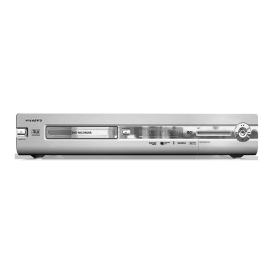
DVD-Video Recorder
Contents
1
Technical Specifications and Connection
Facilities
Diversity Matrix
PCB Locations
2
Safety Information, General Notes
3
Directions for Use
4
Mechanical Instructions
5
Diagnostic Software
6
Block Diagrams, Waveforms, Wiring Diagram
Wiring Diagram
Waveforms
Testpoints
7
Circuit Diagrams and PWB Layouts
Display Panel(Diagram 1)
Front Connector (FC)(Diagram 2)
Standby Panel (STBY)(Diagram 3)
Analog Board:Fronted Video (FV)(Diagram 1)
Analog Board: In / Out Video (IOV)(Diagram 2)
Analog Board: In / Out Audio (IOA)(Diagram 3)
Analog Board: Power Supply (PS)(Diagram 4)
Analog Board: Multi Sound Processing (MSP)
Analog Board: VPS
Analog Board: Follow Me (FOME) (Diagram 7) 92
Analog Board: Digital In/Out (DIGIO)(Diagram 8) 93
Analog Board: Audio Converter (DAC_ADC)
©
Copyright 2004 Philips Consumer Electronics B.V. Eindhoven, The Netherlands.
All rights reserved. No part of this publication may be reproduced, stored in a
retrieval system or transmitted, in any form or by any means, electronic,
mechanical, photocopying, or otherwise without the prior permission of Philips.
Published by GH 0493 Service PaCE
Page
2
2
2
5
7
38
41
43
75
76
78
51
81
82
86
87
88
89
90
(Diagram 5) 91
(Diagram 6) 92
(Diagram 9) 94
Printed in the Netherlands
Contents
UP Sub Board: Central Controler (CECO)
UP Sub Board: Fan Control(FACO)(Diagram 11) 100
In/Out Extension Board (IOE)
DB Chrysalis 2.1: IDE, UARTS, RESET, BE
DB Chrysalis 2.1: 1394
DB Chrysalis 2.1: Audio PLL
DB Chrysalis 2.1: Chrysalis
DB Chrysalis 2.1: 1.8V Power
DB Chrysalis 2.1: Prog. scan DAC(Diagram 6)
DB Chrysalis 2.1: Flash SDRAM EEPROM
DB Chrysalis 2.1: Video IO
DB Chrysalis 2.1: VIPs
8
Alignments
9
Circuit-, IC Descriptions and List
of Abbreviations
10 Spare Parts List
For repair information on the Basic Engine, refer to Service Manual
DVD+RW VAD8041, 12NC: 3122 785 14850.
Subject to modification
DVDR730/0x
Page
(Diagram 10) 99
(Diagram 12) 103
(Diagram 1)
105
(Diagram 2)
106
(Diagram 3)
107
(Diagram 4)
108
(Diagram 5)
109
110
(Diagram 7)
111
(Diagram 8)
112
(Diagram 9)
113
117
120
150
EN 3122 785 14230
Advertisement

Related Manuals for Philips DVDR730/0x


Summary of Contents for Philips DVDR730/0x
- Page 1 All rights reserved. No part of this publication may be reproduced, stored in a retrieval system or transmitted, in any form or by any means, electronic, mechanical, photocopying, or otherwise without the prior permission of Philips. Published by GH 0493 Service PaCE...
-
Page 2: Card Reader
(video unweighted ) Power consumption low power stand-by : < 3 W 1.4.5 Video Performance: RF Tuner Channel 25 / 503,25 MHz, Test pattern: PAL BG PHILIPS standard test pattern, RF Level 74 dBV Test equipment:Fluke 54200 TV Signal generator... - Page 3 (L+R) output: : 100 Hz - 12 kHz / 0± S/N according to DIN 45405, 7, 1967 : Pin Signals: and PHILIPS standard test pattern 1 - Audio R 1.8V RMS FM: ≥ 50dB; AM ≥ video signal: 2 - Audio R ...
- Page 4 EN 4 DVDR730/0x Technical Specifications and Connection Facilities Audio Performance CD 1.12 Dimensions and Weight 1.7.1 Cinch Output Rear Height of feet : 10mm Apparatus tray closed : WxDxH :435 x 324.5 x : 2Vrms ± 2dB 88cm Output voltage 2 channel mode...
- Page 5 Safety Information, General Notes DVDR730/0x EN 5 2. Safety Information, General Notes Description of the Production Number on the Safety regulations require that after a repair, you must return the unit in its original condition. Pay, in particular, attention to...
- Page 6 EN 6 DVDR730/0x Safety Information, General Notes – Wristband tester 4822 344 13999. intellectual property rights owned by Macrovision Corporation • Be careful during measurements in the live voltage section. and other rights owners. The primary side of the power supply (pos. 1005), including...
- Page 7 Directions For Use DVDR730/0x EN 7 Directions For Use...
- Page 8 EN 8 DVDR730/0x Directions For Use...
- Page 9 Directions For Use DVDR730/0x EN 9...
- Page 10 EN 10 DVDR730/0x Directions For Use...
- Page 11 Directions For Use DVDR730/0x EN 11...
- Page 12 EN 12 DVDR730/0x Directions For Use...
- Page 13 Directions For Use DVDR730/0x EN 13...
- Page 14 EN 14 DVDR730/0x Directions For Use...
- Page 15 Directions For Use DVDR730/0x EN 15...
- Page 16 EN 16 DVDR730/0x Directions For Use...
- Page 17 Directions For Use DVDR730/0x EN 17...
- Page 18 EN 18 DVDR730/0x Directions For Use...
- Page 19 Directions For Use DVDR730/0x EN 19...
- Page 20 EN 20 DVDR730/0x Directions For Use...
- Page 21 Directions For Use DVDR730/0x EN 21...
- Page 22 EN 22 DVDR730/0x Directions For Use...
- Page 23 Directions For Use DVDR730/0x EN 23...
- Page 24 EN 24 DVDR730/0x Directions For Use...
- Page 25 Directions For Use DVDR730/0x EN 25...
- Page 26 EN 26 DVDR730/0x Directions For Use...
- Page 27 Directions For Use DVDR730/0x EN 27...
- Page 28 EN 28 DVDR730/0x Directions For Use...
- Page 29 Directions For Use DVDR730/0x EN 29...
- Page 30 EN 30 DVDR730/0x Directions For Use...
- Page 31 Directions For Use DVDR730/0x EN 31...
- Page 32 EN 32 DVDR730/0x Directions For Use...
- Page 33 Directions For Use DVDR730/0x EN 33...
- Page 34 EN 34 DVDR730/0x Directions For Use...
- Page 35 Directions For Use DVDR730/0x EN 35...
- Page 36 EN 36 DVDR730/0x Directions For Use...
- Page 37 Directions For Use DVDR730/0x EN 37...
-
Page 38: See Picture
EN 38 DVDR730/0x Mechanical Instructions 4. Mechanical Instructions Dismantling and Assembly of the Set Remark: Exploded views can be found in chapter 10. 4.1.1 Manually opening the tray – In case the loader is defective or cannot be opened electrically you can open the tray manually. - Page 39 Mechanical Instructions DVDR730/0x EN 39 4.1.3 Digital Board – Unplug the IDE cable that connects to the card reader (1), see picture 4-8 – Remove the 2 screws (2) that fix the card reader – Remove the card reader PCB (3) –...
- Page 40 EN 40 DVDR730/0x Mechanical Instructions Figure 4-14 Figure 4-15...
-
Page 41: Ds_Dcb_Communicationecho_Nuc
Diagnostic Software DVDR730/0x EN 41 5. Diagnostic Software Due to the complexity of the DVD recorder, the time to find a 5.1.2 Structure defect in the recorder can become long. To reduce this time, the recorder has been equipped with Diagnostic and Service software (DS). -
Page 42: Figure
EN 42 DVDR730/0x Diagnostic Software Trade Mode 5.4.2 Error Handling Each nucleus returns an error code. This code contains six numerals, which means: TRADE MODE When the recorder is in Trade Mode, the recorder cannot be controlled by means of the front key buttons, but only by means [ XX YY ZZ ] of the remote control. -
Page 43: Figure
Diagnostic Software DVDR730/0x EN 43 Error messages startup Diversity String Input 1. Execute nucleus 1226 to enter the string. Please see adjustment instructions in chapter 8 for details Nucleus 1226 execution with string Figure 5-6 Error messages D&S program Figure 5-9 1. - Page 44 EN 44 DVDR730/0x Diagnostic Software Chrysalis (CHR) Nucleus Name DS_CHR_DevTypeGet Nucleus Number Description Sends the device ID and the module ids and revisions of the PNX7100 (Chrysalis) to the stdout port. User Input None Example DS:> 100 Device ID 7100 Codec ID PNX7100_MF2 F-BCU (0x0102) 1.0 INTC (0x011d) 1.0 PCI-XIO(0x0113) 1.0...
-
Page 45: Dvdr730/0X 5. En
Diagnostic Software DVDR730/0x EN 45 Example DS:> 102 010200: Test OK @ Nucleus Name DS_CHR_SineOn Nucleus Number Description Generate an audio sine signal on the audio output of the digital board. Note: Left channel 6kHz, right channel 12 kHz sine. Make sure to route the signal first. - Page 46 EN 46 DVDR730/0x Diagnostic Software Nucleus Name DS_CHR_MacroVisionOn Nucleus Number Description Turn on MacroVision. User Input None Example DS:> 110 011000: Test OK @ Nucleus Name DS_CHR_MacroVisionOff Nucleus Number Description Turn off MacroVision. User Input None Example DS:> 111 011100:...
- Page 47 Diagnostic Software DVDR730/0x EN 47 Example DS:> 201 020100: Test OK @ NVRAM Nucleus Name DS_NVRAM_Communication Nucleus Number Description Check the communication between the IIC controller of the Chrysalis and the EEPROM User Input None Example DS:> 300 030000: Test OK @...
- Page 48 EN 48 DVDR730/0x Diagnostic Software Description Check all data lines and address lines of the SDRAM User Input None Example DS:> 401 040100: Test OK @ Nucleus Name DS_SDRAM_Write Nucleus Number Description Write to a specific memory address User Input...
- Page 49 Diagnostic Software DVDR730/0x EN 49 Nucleus Name DS_FLASH_CalculateChecksum Nucleus Number Description Calculate the checksum over all memory addresses. Used to check entire FLASH contents User Input None Example DS:> 504 050400: The Checksum = 0xBABE30A4 Test OK @ Nucleus Name...
- Page 50 EN 50 DVDR730/0x Diagnostic Software Example DS:> 604 1 060400: Test OK @ Digital Video Input Output (DVIO) Nucleus Name DS_DVIO_LinkDevTypeGet Nucleus Number Description Get the device (revision) type information of the 1394 Link layer IC User Input None Example DS:>...
- Page 51 Diagnostic Software DVDR730/0x EN 51 Progressive Scan (PSCAN) Nucleus Name DS_PSCAN_CommunicationDenc Nucleus Number Description Check the communication between the IIC controller of the chrysalis and the progressive scan DENC-IC User Input None Example DS:> 801 080100: Test OK @ Nucleus Name...
- Page 52 EN 52 DVDR730/0x Diagnostic Software Nucleus Name DS_PSCAN_DevTypeGetDeinterlacer Nucleus Number Description Get the device (revision) type information of the progressive scan deinterlacer. User Input None Example DS:> 807 080700: Chip name : 2300 Chip version : 1 Test OK @...
- Page 53 Diagnostic Software DVDR730/0x EN 53 User Input None Example DS:> 905 090500: Test OK @ Nucleus Name DS_BE_WriteReadDvdRw Nucleus Number Description Write data to and read data from a DVD+RW disc through the basic engine for verification of the writing...
- Page 54 EN 54 DVDR730/0x Diagnostic Software Nucleus Name DS_BE_ErrorLogReset Nucleus Number Description Reset the error log in the basic engine User Input None Example DS:> 911 091100: Test OK @ Nucleus Name DS_BE_JitterOptimise Nucleus Number Description Perform jitter optimisation:A formatted DVD must be loaded into the engine before...
- Page 55 Diagnostic Software DVDR730/0x EN 55 Nucleus Name DS_BE_RadialCalibration Nucleus Number Description Calibrate the radial loop User Input A formatted DVD must be loaded into the engine before executing this nucleus Example DS:> 919 091900: Test OK @ Nucleus Name DS_BE_Tilt...
- Page 56 EN 56 DVDR730/0x Diagnostic Software Example DS:> 925 The entirely disc will be erased. Are you sure you want this?[y/n] 092500: Test OK @ Nucleus Name DS_BE_RegionCodeSet Nucleus Number Description Set the region code in the AV3. User Input Region code Example DS:>...
- Page 57 Diagnostic Software DVDR730/0x EN 57 User Input None Example DS:> 1001100100: DCB version: 13Test OK @ Nucleus Name DS_DCB_LightDisplay Nucleus Number 1002 Description Light the entire display of the DCB, and clear the display after confirmation.User confirmation is necessary. User Input...
- Page 58 EN 58 DVDR730/0x Diagnostic Software Example DS:> 1102 110200: Test OK @ Nucleus Name DS_ANAB_CommunicationIicDataSlicer Nucleus Number 1103 Description Check the communication between the digital board and the data slicer on the analogue board User Input None Example DS:> 1103...
- Page 59 Diagnostic Software DVDR730/0x EN 59 Nucleus Name DS_ANAB_SoftwareVersionDiagnosticsGet Nucleus Number 1110 Description Get the software version of the diagnostic software of the analogue board User Input None Example DS:> 1110 111000: Diagnostics application version : 11.00.13 Test OK @ Nucleus Name...
- Page 60 EN 60 DVDR730/0x Diagnostic Software Input signal is from REAR VIDEO(CVBS) IN and will be routed to the digital board. Input signal is from FRONT S-VIDEO(Y/C) IN and the signal received will be routed to the digital board. Input signal is from REAR S-VIDEO(Y/C) IN and will be routed to the digital board.
- Page 61 Diagnostic Software DVDR730/0x EN 61 Input Audio Signal is routed from FRONT Cinch In to Digital Board.(This is same as path ID Input Signal is from Rear Cinch In1 and it will be routed to Digital Board.. No routing. No routing.
- Page 62 EN 62 DVDR730/0x Diagnostic Software Nucleus Name DS_ANAB_ClockReference Nucleus Number 1117 Description Generate a 1 kHz signal on pin 7 (INT) of the clock IC User Input None Example DS:> 1117 111700: Test OK @ Nucleus Name DS_ANAB_ClockCorrection Nucleus Number...
- Page 63 Diagnostic Software DVDR730/0x EN 63 Byte containing 8 bit fields for TRUE/FALSE : BIT 0: Decoder BIT 1: Modulation BIT 2: NICAM NICAM/stereo bit for Europe SAP/stereo bit for NAFTA BIT 3: Satpreset BIT 4: Presetdefined Preset defined bit is only used for Europe. For NAFTA,...
- Page 64 EN 64 DVDR730/0x Diagnostic Software Example DS:> 1204 120400: Software Diagnostics Version = 0001 Test OK @ Nucleus Name DS_SYS_EepromUpload Nucleus Number 1205 Description Upload the contents of the NVRAM on the analogue board or the digital board to the...
- Page 65 Diagnostic Software DVDR730/0x EN 65 Example DS:> 1210 0 0xa0 1 121000: Value read =0x06T est OK @ Nucleus Name DS_SYS_UartWrite Nucleus Number 1211 Description Perform an UART write action on the digital board on a specified UART User Input The user inputs the UART to write to, the number of bytes and the bytes to be written to the UART.
- Page 66 EN 66 DVDR730/0x Diagnostic Software Example DS:> 1215 cvbs ntsc 121500: Test OK @ DS:> 1215 cvbs pal 121508: The VideoInputProcessor cannot detect a sync-signal. Error @ DS:> 1215 yuv ntsc 121511: Error in luminance signal(Y) Error in chrominance signal(U)
- Page 67 Diagnostic Software DVDR730/0x EN 67 Nucleus Name DS_SYS_DisplayFatalOn Nucleus Number 1223 Description Turn on the display-fatal functionality which displays debug-information on the display when encountering a fatal error condition from which could not be recovered automatically User Input None Example DS:>...
- Page 68 EN 68 DVDR730/0x Diagnostic Software Example DS:> 1229 122900: 6D7920626F61726400020300010101020101000020080000 Test OK @ Nucleus Name DS_SYS_AudioLoopThroughStart Nucleus Number 1230 Description Description: The audio input is routed from the an input to all outputs. Input is set with the routing nucleus 1113. All outputs are enabled.
- Page 69 Diagnostic Software DVDR730/0x EN 69 Nucleus Name DS_SYS_SettingsDoubleCheck Nucleus Number 1233 Description This nucleus sets the HW-Id in the HW-diversity string User Input <HW-ID> - The hardware ID to set -No input - The user will be asked for the ID Example DS:>...
- Page 70 EN 70 DVDR730/0x Diagnostic Software HARD DISK DRIVE (HDD) Nucleus Name DS_HDD_SpinOff Nucleus Number 2110 Description Put the HDD in parking position by sending the sleep command so it can be moved without endangering the mechanical parts User Input None...
- Page 71 Diagnostic Software DVDR730/0x EN 71 Example DS:> script Executing User/Dealer script. Busy executing NUC1100 1-28 Hello Analogue Board Busy executing NUC1000 2-28 Busy executing NUC200 3-28 Busy executing NUC1228 4-28 Settings ID: 4C4541440D00000000030300010101020101000020080000 Board name: LEAD Hardware ID: 0 Codec IC: PNX7100_MF3...
- Page 72 EN 72 DVDR730/0x Diagnostic Software Example Busy executing NUC601 16-28 Busy executing NUC700 17-28 Device type of the link layer IC: ffc00301 Busy executing NUC701 18-28 Device type of the phy layer IC: 0 Busy executing NUC702 19-28 Busy executing NUC703 20-28...
-
Page 73: Diagram
Block Diagrams, Waveforms, Wiring Diagram. DVDR730/0x EN 73 6. Block Diagrams, Waveforms, Wiring Diagram. Overall Block Diagram Digital Board 2.1 Chrysalis ANALOG BOARD INTELLIGENT CONTROL UP SUB BOARD 1942 FRONT 1922 AUDIO L Analog input AFCRI AFCRI AUDIO R AFCLI... - Page 74 Block Diagrams, Waveforms, Wiring Diagram. DVDR730/0x EN 74 Control Block Diagram Analog Board, uP Board DVIO-Board Digital Board Basic Engine DVIO Digital Board BE_FAN P-Subprint BE_FAN Sense 3V3STBY A0-A7 A0-A7 A_DATA Fan_off Reset-IC ext. Latch ext. RAM ext. Flash D_DATA...
- Page 75 Block Diagrams, Waveforms, Wiring Diagram. DVDR730/0x EN 75 Wiring Diagram 1 mm GNDD GNDA FBIN 1951 1944 1941 BE_FAN GNDA DVDR 80 EUROPE 1949 1948 N.C. GNDA D_RDY 1 mm A_RDY GNDA D_DATA A_DATA 1 mm F4709 1 mm (1005) IRESET_DIG N.C.
- Page 76 Block Diagrams, Waveforms, Wiring Diagram. DVDR730/0x EN 76 Waveforms Waveforms Analog Board Waveforms Display Board I324 VGate (no disc loaded) 7106/7108-Emitter IC7103-8 F327 VDrain (Standby) I324 VGate (Standby) IC7103-19 F327 VDrain (no disc loaded) A: DC, 1 V/Div, 10us/Div A: DC, 1 V/Div, 100ns/Div...
- Page 77 Block Diagrams, Waveforms, Wiring Diagram. DVDR730/0x EN 77 Waveforms Digital Board Chrysalis 2.1 HS_IN IC7703 pin 36 Y 1704-2 IC7703 pin 34 PB 1704-4 PR 1704-6 A: DC, 200mV/Div, 5us/Div A: DC, 2 V/Div, 10us/Div A: DC, 200mV/Div, 5us/Div A: DC, 500mV/Div...
- Page 78 Block Diagrams, Waveforms, Wiring Diagram. DVDR730/0x EN 78 Test points overview Analog Board I732 A3 F0001 A10 F301 A3 F321 C3 F343 A2 F363 A2 F4205 C6 F5102 A5 F5216 C8 I004 C10 I036 A9 I319 C3 I339 A2 I361 A2...
- Page 79 Block Diagrams, Waveforms, Wiring Diagram. DVDR730/0x EN 79 Test points overview UP Sub Board F8001 C3 F831 C1 F8610 C3 I808 A3 F8002 C3 F832 A2 F8701 A1 I809 C1 F8003 C3 F833 C1 F8702 A3 I810 B3 F8004 C3...
- Page 80 Block Diagrams, Waveforms, Wiring Diagram. DVDR730/0x EN 80 Test points overview Digital Board I504 C1 I745 A5 F0001 C1 F0238 D1 F1510 B1 I009 A1 I227 B3 I300 B3 I505 C1 I746 A2 F0003 C1 F0239 D1 F1512 A1 I010 A1...
- Page 81 Circuit Diagrams and PWB Layouts DVDR730/0x EN 81 7. Circuit Diagrams and PWB Layouts Display Panel 0005 B4 F1408 G2 0206 B4 F1409 H2 0210 C1 F1410 H2 0803 A1 F1503 H1 1110 D9 F1504 I1 1165 I6 I100 E12...
- Page 82 Circuit Diagrams and PWB Layouts DVDR730/0x EN 82 Front Connector (FC) 1920 B1 1921 E1 1922 C9 2200 A5 2201 C5 3200 2202 E3 2203 C6 3200 A5 3201 A6 CINCH 3202 B5 3203 C6 3204 C5 F1006 3205 C3...
- Page 83 Circuit Diagrams and PWB Layouts DVDR730/0x EN 83 Layouts Display Panel Part 1 TR 13005a_001 Part 2 TR 13005b_001 TR 13005_001 200803...
- Page 84 Circuit Diagrams and PWB Layouts DVDR730/0x EN 84 Layout Display Panel (Part 1 Bottom View) TR 13005a_001 200803...
- Page 85 Circuit Diagrams and PWB Layouts DVDR730/0x EN 85 Layout Display Panel (Part 2 Bottom View) TR 13005b_001 200803...
- Page 86 Circuit Diagrams and PWB Layouts DVDR730/0x EN 86 Standby Panel (STBY) Layout Standby Panel 1130 B3 1930 A2 3300 B3 F3003 A2 F3004 A2 I300 B3 1930 F3003 Tray_Led F3004 not used TR 13006_001 210803 TR 13004_001 200803...
- Page 87 Circuit Diagrams and PWB Layouts DVDR730/0x EN 87 Analog Board: Frontend Video (FV) 0005 A1 1703 D7 2713 A3 2722 B8 2727 C8 2731 C9 2735 G1 2741 F4 3703 A3 3711 A4 3717 E12 3726 C5 3732 E15 3736 F15...
- Page 88 Circuit Diagrams and PWB Layouts DVDR730/0x EN 88 Analog Board: In/Out Video (IOV) 1940-1 A8 6418 B12 1940-2 A13 6419 B10 1940-3 A14 6420 A5 1942 E1 6422 A11 1943 C1 6423 A8 1945-1 I2 6424 B10 1947 I7 6425 G13...
- Page 89 Circuit Diagrams and PWB Layouts DVDR730/0x EN 89 Analog Board: IN/Out Audio (IOA) 2501 A5 I503 B1 2502 A6 I504 D1 2503 A2 I505 B2 5VSTBY 5VSTBY 2504 A1 I506 B2 5NSTBY 5VSTBY 2505 A1 I507 C3 2506 A4 I508 E4...
- Page 90 Circuit Diagrams and PWB Layouts DVDR730/0x EN 90 Analog Board: Power Supply (PS) 1300 A2 3360 G5 F344 G14 1301 B2 3361 F12 F346 E13 1302 A3 3362 H10 F347 E13 1303 E9 3363 G8 F348 G2 1304 C9 3364 G8...
- Page 91 Circuit Diagrams and PWB Layouts DVDR730/0x EN 91 Analog Board: Multi Sound Processing (MSP) 1600 F7 1960 E1 2600 A6 2601 A6 2602 A7 I601 2603 A7 2604 A9 2605 F5 3600 2606 B8 I603 5SW1 2607 C2 I602 I624...
- Page 92 Circuit Diagrams and PWB Layouts DVDR730/0x EN 92 Analog Board: VPS Analog Board: Follow Me (FOME) 2940 A2 2944 D4 3937 C1 3941 D3 3945 E3 3950 A3 3954 C2 7934-B B4 I951 B3 I956 D2 2941 B3 2945 D2...
- Page 93 Circuit Diagrams and PWB Layouts DVDR730/0x EN 93 Analog Board: Digital In / Out (DIGIO) 1951 A4 2585 C3 2590 A3 3582 D2 5580 A2 7580-A C2 7580-D D3 F4102 A4 I488 C2 I491 D2 2580 A3 2586 D3 3580 A3...
- Page 94 Circuit Diagrams and PWB Layouts DVDR730/0x EN 94 Analog Board: Audio Converter (DAC_ADC) 1001 H10 F0011 E2 1900 C2 F0012 E2 2000 H13 F0014 D2 2001 H13 F0016 D2 2002 B7 F0021 C2 5VSTBY 2003 B7 F006 H11 2004 B7...
- Page 95 Circuit Diagrams and PWB Layouts DVDR730/0x EN 95 Layout Analog Board (Top View) 0005 A8 1702 B7 1943 A1 2313 C8 2344 B9 2461 B5 2608 B4 3019 C1 3322 A9 3447 A7 5404 B4 6003 C3 6316 C10 7317 A8...
- Page 96 Circuit Diagrams and PWB Layouts DVDR730/0x EN 96 Layout Analog Board (Overview Bottom View) 2003 B10 2023 B10 2049 A9 2337 C1 2412 A9 2437 B6 2503 A9 2523 A6 2603 B6 2723 B4 2935 A10 3008 B10 3024 B9...
- Page 97 Circuit Diagrams and PWB Layouts DVDR730/0x EN 97 Layout Analog Board (Part 1 Bottom View) TR 17025a_001 250204...
- Page 98 Circuit Diagrams and PWB Layouts DVDR730/0x EN 98 Layout Analog Board (Part 2 Bottom View) 17025b_001 230204...
- Page 99 Circuit Diagrams and PWB Layouts DVDR730/0x EN 99 UP Sub Board: Central Controller (CECO) 0606 B15 2801 B8 2810 B3 2819 A5 2828 H13 3801 A8 3810 E10 3819 G15 3828 F13 3837 B4 3846 A4 3856 F3 3866 A2...
- Page 100 Circuit Diagrams and PWB Layouts DVDR730/0x EN 100 UP Sub Board: Fan Control (FACO) 1301 B4 3915 C3 3922 C1 3929 A4 4902 D3 7902-2 D2 7907 A2 F904 B4 I903 C2 1901 A4 3916 D1 3923 E1 3930 A4...
- Page 101 Circuit Diagrams and PWB Layouts DVDR730/0x EN 101 Layout UP Sub Board (Top View) TR 06012_001 040203...
- Page 102 Circuit Diagrams and PWB Layouts DVDR730/0x EN 102 Layout UP Sub Board (Bottom View) 1301 A1 3826 C2 3918 B1 2801 C2 3827 A3 3920 B1 2802 C2 3829 C2 3923 A1 2803 B3 3833 A2 3925 B1 2806 A3...
- Page 103 Circuit Diagrams and PWB Layouts DVDR730/0x EN 103 In/Out Extension Board IOE 0006 A1 1922-C C10 2250 A1 2256 B4 2262 E4 3252 A3 3258 B2 3264 D4 3273 B9 5254 A9 6256 D8 7250-3 C2 F2004 E1 F2203 D10...
- Page 104 Circuit Diagrams and PWB Layouts DVDR730/0x EN 104 Layout In / Out Extension Board TR 06037_00 1 06020 3...
- Page 105 Circuit Diagrams and PWB Layouts DVDR730/0x EN 105 Digital Board Chrysalis 2.1: IDE, UARTS, RESET, BE 1100 A10 4117 E6 1102 B14 4118 F8 1103 H14 4119 F8 1104 G9 4121 H6 VDD_PNX_PAD 1105 B10 4122 B5 2108 1106 I5...
- Page 106 Circuit Diagrams and PWB Layouts DVDR730/0x EN 106 Digital Board Chrysalis 2.1: 1394 1201 D1 3289 H13 1203 A1 3290 I13 2200 B2 3291 I13 2201 C2 3292 I13 2202 D1 3293 I13 +3V3_IEEE_A +3V3_IEEE_PLL +3V3_IEEE_D +3V3_IEEE_D +3V3_LINK +3V3_IEEE_D +3V3_IEEE_D...
- Page 107 Circuit Diagrams and PWB Layouts DVDR730/0x EN 107 Digital Board Chrysalis 2.1: Audio PLL 2300 A3 2301 A4 2302 B2 2303 C1 4304 2304 B4 PLL_OUT 2305 C1 not used 2306 C2 FSCLK3_OUT 2307 E3 I300 5300 4314 2308 F7...
- Page 108 Circuit Diagrams and PWB Layouts DVDR730/0x EN 108 Digital Board Chrysalis 2.1: Chrysalis 1400 C14 3490 E11 1401 I5 3491 E10 2400 A9 3492 E11 PCI_AD(31:0) 2401 A9 3493 E10 PCI_CON VDD_PNX_PAD 2402 A9 3494 E11 SDRAM I418 3400 2403 A12...
- Page 109 Circuit Diagrams and PWB Layouts DVDR730/0x EN 109 Digital Board Chrysalis 2.1: 1.8V Power 12.3V 1.5V 3.8V IC7501 pin 5 IC7501 pin 6 A: DC, 2 V/Div, 1us/Div A: DC, 2 V/Div, 1us/Div TR 19006_001 250504...
- Page 110 Circuit Diagrams and PWB Layouts DVDR730/0x EN 110 Digital Board Chrysalis 2.1: Prog. scan DAC 1704 D13 I727 C9 2700 B4 I728 E8 2701 G11 I729 E9 2703 D5 I730 C2 2704 B4 I731 C2 2705 C5 I732 C2 2706 B2...
- Page 111 Circuit Diagrams and PWB Layouts DVDR730/0x EN 111 Digital Board Chrysalis 2.1: Flash SDRAM EEPROM 0605 E3 0609 F3 2806 A12 2807 A13 2808 A12 +3V3 VDD_NOR 2809 A13 I805 2810 A12 5803 7807 VDD_NOR 2811 A13 7805 PCI_AD(31:0) PCI_AD(31:0)
- Page 112 Circuit Diagrams and PWB Layouts DVDR730/0x EN 112 Digital Board Chrysalis 2.1: Video IO 1900 E14 5913 H4 1901 G13 5914 F10 1904 A14 5915 F10 2036 I5 5916 H13 2046 G12 7900 E9 2900 A4 7901 F9 2901 A4...
- Page 113 Circuit Diagrams and PWB Layouts DVDR730/0x EN 113 Digital Board Chrysalis 2.1: VIPs 1000 B2 F011 D13 1001 G9 F012 F9 2000 B3 F013 H3 2001 B3 F014 H3 I002 2002 B3 F015 H3 3023 VDDA_7118 2003 B4 F016 H3...
- Page 114 Circuit Diagrams and PWB Layouts DVDR730/0x EN 114 Layout Digital Board Chrysalis 2.1 (Top View) 2703 A2 3152 C3 3309 B1 3492 D2 4001 B3 7300 B1 0605 D1 2704 B2 3154 D3 3310 B1 3493 D1 4002 B3 7301 B1...
- Page 115 Circuit Diagrams and PWB Layouts DVDR730/0x EN 115 Layout Digital Board Chrysalis 2.1 (Bottom View) 1000 B1 2405 C3 2941 A2 3277 A2 3928 A1 6000 A1 1201 A3 2406 C2 2942 A2 3279 A2 3932 A1 6100 B2 1401 C3...
- Page 116 Circuit Diagrams and PWB Layouts DVDR730/0x EN 116...
- Page 117 Alignments DVDR730/0x EN 117 8. Alignments Alignment Instructions Analog Board Test equipment: 2 HF - AGC adjustment [3724]: 1. Dual-trace oscilloscope Service tasks after replacement of IC 7710: Voltage range : 0.001 ~ 50 V/div Frequency : DC ~ 50 MHz Purpose: Set amplifier control.
- Page 118 The slash version is stored with command 1217, followed by the slash version as parameter. The NVM, item 7808, on the Microprocessor Sub board The slash versions used in DVDR730/0x are the following: contains the following factory settings: • DVDR730/00/02: 1.
- Page 119 Alignments DVDR730/0x EN 119 – 36 = Production WEEK – 130156 = Lot and SERIAL number 2. Calculate the unique number: this number always exists out of 10 hexadecimal numbers. 3. First 5 numbers: First we calculate a decimal number...
- Page 120 EN 120 DVDR730/0x Circuit-, IC descriptions and list of abbreviations 9. Circuit-, IC descriptions and list of abbreviations Display Board 9.1.7 REC-LED The REC-LED-ring is made with 3 red LED, controlled via pin 9.1.1 Microcontroller 3 (only for flashing) and pin 12 for on/off switching, of the microcontroller.
- Page 121 Circuit-, IC descriptions and list of abbreviations DVDR730/0x EN 121 [1986]). By generating a high level on pin 16 of the CC the 9.3.2 Power Supply Unit digital PCB can be reset (inverter [7817] in between). Most of the other parts are controlled by the µP via I2C-bus Functional principle: (“SDA”- and “SCL”-signal).
- Page 122 EN 122 DVDR730/0x Circuit-, IC descriptions and list of abbreviations The feedback control for the switched-mode power supply is reception, an additional circuit for suppressing the audio carrier done by changing the conductive phase of the switching of the adjacent channel is used. This circuitry is adjusted by coil transistor so that either more or less energy is transferred from [5710] for maximum suppression at 40.4MHz.
- Page 123 Circuit-, IC descriptions and list of abbreviations DVDR730/0x EN 123 9.3.4 Audio routing TR 01055_001 170502...
- Page 124 EN 124 DVDR730/0x Circuit-, IC descriptions and list of abbreviations The processing of audio is always done in stereo (e.g. separate There are two possibilities for a digital audio input signal in case left- and right-channel) and the complete switching is realized of option “DIGITAL IN”.
- Page 125 Circuit-, IC descriptions and list of abbreviations DVDR730/0x EN 125 (clipping) the mute transistors for cinch rear out [7415], [7416] 9.3.6 Video-routing are decoupled via [7011]. Figure 9-1...
- Page 126 EN 126 DVDR730/0x Circuit-, IC descriptions and list of abbreviations The Video-I/O-switching is basically realized by the matrix 9.3.8 Analog Follow-Me switch STV6618 [7408], which is controlled via I C-bus by the CC. All used outputs excluding pin 21 (Y/CVBS-REC) have a 6 This circuit compares the video signal from the internal dB-amplification and a 75 Ohms driver-stage inside.
- Page 127 Circuit-, IC descriptions and list of abbreviations DVDR730/0x EN 127 9.4.2 Audio routing TR 01057_001 170502 Figure 9-2...
- Page 128 EN 128 DVDR730/0x Circuit-, IC descriptions and list of abbreviations The sound processing is always done in stereo (that means DAC-part and “IPFAIL” from the power-supply-unit. The circuit separate left- and right-channel). around [6430], [6431], [7430] and [7404] generates this signal.
- Page 129 Circuit-, IC descriptions and list of abbreviations DVDR730/0x EN 129 9.4.4 Video-routing Figure 9-3...
- Page 130 EN 130 DVDR730/0x Circuit-, IC descriptions and list of abbreviations Digital Board Chrysalis 2.1 The Video-I/O-switching is basically realized by the matrix switch STV6618 [7408], which is controlled via I C-bus by the 9.5.1 Introduction CC. All used outputs excluding pin 21 (Y/CVBS-REC) have a 6dB-amplification and a 75 Ohms-driver-stage inside.
- Page 131 Circuit-, IC descriptions and list of abbreviations DVDR730/0x EN 131 9.5.2 Record Mode Block diagram Chrysalis Digital Board TO/FROM BE AV3 OPTIONAL HDD, PCMCIA BE AV2 IDE CONNECTOR UART I2S EEPROM EEPROM 64Kbit 64Kbit I2C0 I2C 0 I2C 0 7004...
- Page 132 EN 132 DVDR730/0x Circuit-, IC descriptions and list of abbreviations AV3 Basic Engine (VAE8030) 9.5.5 Clock Distribution To be prepared for new developments, the Chrysalis Digital Board is equipped with two IDE busses (ATAPI). They can be Clock distribution on Chrysalis board used for connecting to the new generation Basic Engine (e.g.
- Page 133 Circuit-, IC descriptions and list of abbreviations DVDR730/0x EN 133 9.5.8 Reset Reset concept Chrysalis board Reset_IDEn 7104-3 & Reset_1394n 7400 7104-4 & 7106 NCP303 >1 PNX7100_Resetn Reset_BEn 7107-1 & Reset_PSn 7107-2 CHRYSALIS GPIO & PNX7100 Analog_Resetn 7107-3 & VIP_Resetn 7104-1 &...
- Page 134 EN 134 DVDR730/0x Circuit-, IC descriptions and list of abbreviations Service UART Interface I/O Extension Board Logic IC 74HCT14D (item 7111) is used to make a level This board feeds the internal S/PDIF signal from the Digital conversion from microprocessor (LVTTL) to +/-5V (compatible board to an optical and/or digital out connector.
- Page 135 Circuit-, IC descriptions and list of abbreviations DVDR730/0x EN 135 Figure 9-9...
- Page 136 EN 136 DVDR730/0x Circuit-, IC descriptions and list of abbreviations Figure 9-10...
- Page 137 Circuit-, IC descriptions and list of abbreviations DVDR730/0x EN 137 9.8.2 IC’s Analog Board IC7408: STV6618 Analog Board, Video Switch Matrix Pin Description Pin No. Symbol Description Y/CVBSIN_TUN Y/CVBS Input from Tuner DIGOUT3 Digital Output Pin 3 GND1 Ground Supply 1 for Video Inputs...
-
Page 138: Diagram
EN 138 DVDR730/0x Circuit-, IC descriptions and list of abbreviations Pin No. Symbol Description +5 V Digital Power Supply I²C Bus Clock I²C Bus Data GNDD Digital Ground Supply CIN_TV Chroma Input from TV (SCART1 or external Cinch) Y/CVBSIN_TV Y/CVBS Input from TV (SCART1 or external Cinch) - Page 139 Circuit-, IC descriptions and list of abbreviations DVDR730/0x EN 139 Figure 3: STV6618 Block Diagram DIGOUT6 DIGOUT5 DIGOUT4 DIGOUT3 DIGOUT2 DIGOUT1 C_GATE...
- Page 140 EN 140 DVDR730/0x Circuit-, IC descriptions and list of abbreviations IC7411: NJM2285 Analog Board, Video Switch...
- Page 141 Circuit-, IC descriptions and list of abbreviations DVDR730/0x EN 141 IC7313 TEA 1507 Analog Board, Power Supply Control BLOCK DIAGRAM andbook, full pagewidth...
- Page 142 EN 142 DVDR730/0x Circuit-, IC descriptions and list of abbreviations IC7404: AD1582 Analog Board, Digital/Analogue Converter FUNCTIONAL BLOCK DIAGRAM DIGITAL CLOCK CONTROL DATA SUPPLY INPUT VOLUME MUTE VOLTAGE AUTO-CLOCK SERIAL CONTROL AD1852 REFERENCE DIVIDE CIRCUIT INTERFACE 16-/18-/20-/24-BIT MULTIBIT SIGMA- ATTEN/...
- Page 143 Circuit-, IC descriptions and list of abbreviations DVDR730/0x EN 143 AD1852 PIN FUNCTION DESCRIPTIONS Input/Output Pin Name Description DGND Digital Ground. MCLK Master Clock Input. Connect to an external clock source at either 256 F , 384 F 512 F...
- Page 144 EN 144 DVDR730/0x Circuit-, IC descriptions and list of abbreviations 9.8.3 ICs Digital Board Chrysalis IC7106 NCP303LSN29, Digital Board 2.1 Chrysalis, Reset Circuit NCP303LSNxxT1 Open Drain Output Configuration Input Reset Output...
- Page 145 Circuit-, IC descriptions and list of abbreviations DVDR730/0x EN 145 IC7501 NCP1570D, Digital Board 2.1 Chrysalis, DC/DC Converter Control NCP1570 Fault Latch UVLO COMP – – 8.5 V/7.5 V – Set Dominant 0.25 V – Error Amp – PWM Latch...
- Page 146 EN 146 DVDR730/0x Circuit-, IC descriptions and list of abbreviations IC7703: ADV7302 Digital Board, Multi Format Progressive Scan Video Encoder Block diagram of the ADV7302A/03A HD PIXEL SHARPNESS & Y COLOR INPUT TEST- ADAPTIVE CR COLOR INTER- PATTERN PS 4X...
- Page 147 Circuit-, IC descriptions and list of abbreviations DVDR730/0x EN 147 PIN FUNCTION DESCRIPTIONS Pin Mnemonic Input/Output Function D G N D Digital Ground AGND Analog Ground C L K I N _ B Pixel Clock Input. Requires a 27MHz reference clock for Progressive Scan Mode or a 74.25MHz (74.1758MHz) reference clock in HDTV mode.
- Page 148 EN 148 DVDR730/0x Circuit-, IC descriptions and list of abbreviations 760 Ohms resistor must be connected from this pin to AGND and is used to SET1,2 control the amplitudes of the DAC outputs. S C L Multifunctional input: MPU Port Serial Interface Clock Input.
- Page 149 Circuit-, IC descriptions and list of abbreviations DVDR730/0x EN 149 RY/BY_ Ready/Busy – input line (from Flash- ALRCLK Audio Word Select ROM) AMCLK44 11.2896MHz (=256 * 44.1 kHz) audio SIF1 Sound intermediate frequency master clock signal for 44.1 kHz audio...
- Page 150 EN 150 DVDR730/0x Spare Parts List 10. Spare Parts List 10.1 Exploded View of the Set TR 13012_001 220803 Figure 10-1...
- Page 151 Spare Parts List DVDR730/0x EN 151 10.2 Exploded View of the Front Panel Complete TR 13013_001 220803 Figure 10-2...
- Page 152 EN 152 DVDR730/0x Spare Parts List 10.3 Exploded View of the Front without PWBs Figure 10-3...
- Page 153 Spare Parts List DVDR730/0x EN 153 2202 2238 586 59812 100nF 20-80% 50V 0603 7107 9322 185 95667 TSOP4836 Mechanical 7108 4822 130 41246 BC327-25 7109 3198 010 42310 BC847BW 7112 4822 130 60854 DTA124EU-W Various 3100 4822 051 30223 22kΩ 5% 0.062W 3101 4822 051 30223 22kΩ...
- Page 154 Spare Parts List DVDR730/0x EN 154 2306 2020 021 91528 560µF 6V3 20% 2509 2238 586 59812 100nF 20-80% 50V 0603 3012 4822 051 30103 10kΩ 5% 0.062W 2307 4822 122 31175 1nF 10% 500V 2510 4822 124 42234 100µF 20% 6,3V 3013 5322 117 13053 6.8kΩ...
- Page 155 Spare Parts List DVDR730/0x EN 155 3357 4822 051 30472 4.7kΩ 5% 0.062W 3477 4822 051 30101 100Ω 5% 0.062W 3939 4822 051 30472 4.7kΩ 5% 0.062W 3358 4822 051 30109 10Ω 5% 0.062W 3478 4822 051 30101 100Ω 5% 0.062W 3940 3198 021 31060 10MΩ...
- Page 156 EN 156 DVDR730/0x Spare Parts List 5931 4822 157 11706 10µH 5% 7319 5322 130 60159 BC846B 2823 5322 126 11578 1nF 10% 50V 0603 5932 2422 549 43062 Bead 600Ω at 100MHz 7320 9322 163 75685 SI2306DS 2824 3198 017 41050 1µF 10V 0603...
- Page 157 Spare Parts List DVDR730/0x EN 157 3887 4822 051 30472 4.7kΩ 5% 0.062W 1901 2422 025 16987 CON V 6P F 2308 2238 586 59812 100nF 20-80% 50V 0603 3888 4822 051 30471 470Ω 5% 0.062W 1904 2422 025 16389 CON V 22P F...
- Page 158 EN 158 DVDR730/0x Spare Parts List 2909 2238 586 59812 100nF 20-80% 50V 0603 3149 4822 117 12139 22Ω 5% 0.062W 3278 4822 051 30221 220Ω 5% 0.062W 2910 3198 016 31510 150pF 10% 50V 0603 3154 2322 702 60829 82Ω 5% 0603 3279 4822 051 30221 220Ω...
- Page 159 Spare Parts List DVDR730/0x EN 159 3470 4822 117 12139 22Ω 5% 0.062W 3868 4822 117 11817 1.2kΩ 1% 1/16W 5502 4822 157 11499 BLM11P600SPT 3471 4822 117 12139 22Ω 5% 0.062W 3869 4822 051 30472 4.7kΩ 5% 0.062W 5503 2422 535 94995 10µH 1014520%...
- Page 160 EN 160 DVDR730/0x Spare Parts List 2250 3198 017 41050 1µF 10V 0603 2254 4822 122 33753 150pF 5% 50V 2255 2238 586 59812 100nF 20-80% 50V 0603 2256 2238 586 59812 100nF 20-80% 50V 0603 2257 5322 126 11578 1nF 10% 50V 0603...