Table of Contents
Advertisement
Notes: Please use this manual together with service manual
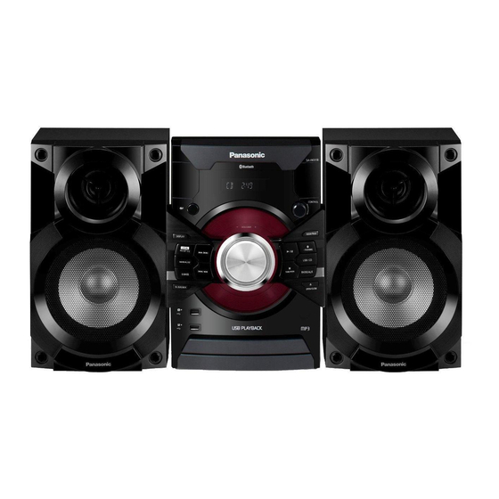
Model No.[SA-AKX18PN-K], Order no. (PSG1401007CE).
Speaker system SB-AKX18P-K, Order No. PSG1406006AE
TABLE OF CONTENTS
1 Safety Precautions----------------------------------------------- 3
1.1. General Guidelines---------------------------------------- 3
1.2. Before Repair and Adjustment ------------------------- 3
1.3. Protection Circuitry ---------------------------------------- 4
1.4. Power Supply using SMPS ----------------------------- 4
1.5. Safety Parts Information --------------------------------- 5
2 Warning -------------------------------------------------------------- 6
Model No.
Product Color: (K)...Black Type
PAGE
to Electrostatically Sensitive (ES) Devices ----------6
2.2. Precaution of Laser Diode -------------------------------6
(PbF) ---------------------------------------------------------- 7
2.4. Handling Precautions for Traverse Unit --------------7
prevention----------------------------------------------------8
© Panasonic Corporation 2014. All rights reserved.
Unauthorized copying and distribution is a violation of
law.
CD Stereo System
SA-AKX18P
PSG1405011AE
A6
PAGE
Advertisement
Table of Contents

Related Manuals for Panasonic SA-AKX18P


Summary of Contents for Panasonic SA-AKX18P
-
Page 1: Table Of Contents
(PbF) ---------------------------------------------------------- 7 1.5. Safety Parts Information --------------------------------- 5 2.4. Handling Precautions for Traverse Unit --------------7 2 Warning -------------------------------------------------------------- 6 2.5. Grounding electrostatic breakdown prevention----------------------------------------------------8 © Panasonic Corporation 2014. All rights reserved. Unauthorized copying and distribution is a violation of law. - Page 2 3 Service Navigation------------------------------------------------9 3.1. Service Information ----------------------------------------9 3.2. Notes ----------------------------------------------------------9 3.3. Different Points ------------------------------------------- 10 4 Specifications ---------------------------------------------------- 11 5 Block Diagram --------------------------------------------------- 13 5.1. Audio -------------------------------------------------------- 13 6 Schematic Diagram--------------------------------------------- 14 6.1. Main (Damp) Circuit ------------------------------------- 14 6.2. Main (Tuner / AUX) Circuit----------------------------- 15 6.3.
-
Page 3: Safety Precautions
1 Safety Precautions 1.1. General Guidelines 1. IMPORTANT SAFETY NOTICE There are special components used in this equipment which are important for safety. These parts are marked by in the Schematic Diagrams, Circuit Board Layout, Exploded Views and Replacement Parts List. It is essential that these critical parts should be replaced with manufacturer’s specified parts to prevent X-RADIATION, shock, fire, or other hazards. -
Page 4: Protection Circuitry
Figure 1-2 Caution: DO NOT SHORT-CIRCUIT DIRECTLY (with a screwdriver blade, for instance), as this may destroy solid state devices. After repairs are completed, restore power gradually using a variac to avoid overcurrent. Current consumption at AC 120 V, 60 Hz in Power ON, FM Tuner at volume minimal mode should be ~ 250 mA. 1.3. -
Page 5: Safety Parts Information
Figure 1-3 1.5. Safety Parts Information Safety Parts List: There are special components used in this equipment which are important for safety. These parts are marked by in the Schematic Diagrams, Exploded View & Replacement Parts List. It is essential that these critical parts should be replaced with manufacturer’s specified parts to prevent shock, fire or other hazards. -
Page 6: Warning
2 Warning 2.1. Prevention of Electrostatic Discharge (ESD) to Electrostatically Sensi- tive (ES) Devices Some semiconductor (solid state) devices can be damaged easily by static electricity. Such components commonly are called Elec- trostatically Sensitive (ES) Devices. The following techniques should be used to help reduce the incidence of component damage caused by electrostatic discharge (ESD). -
Page 7: General Description About Lead Free Solder (Pbf)
Figure 2-1 2.3. General description about Lead Free Solder (PbF) The lead free solder has been used in the mounting process of all electrical components on the printed circuit boards used for this equipment in considering the globally environmental conservation. The normal solder is the alloy of tin (Sn) and lead (Pb). -
Page 8: Grounding For Electrostatic Breakdown Prevention
ble cable, cut off the antistatic FPC. Figure 2-2 2.5. Grounding for electrostatic breakdown prevention • As for parts that use optical pick-up (laser diode), the optical pick-up is destroyed by the static electricity of the working environ- ment. Repair in the working environment that is grounded. 2.5.1. -
Page 9: Service Navigation
3 Service Navigation 3.1. Service Information This service manual contains technical information which will allow service personnel’s to understand and service this model. Please place orders using the parts list and not the drawing reference numbers. If the circuit is changed or modified, this information will be followed by supplement service manual to be filed with original service manual. -
Page 10: Different Points
3.3. Different Points Ref. No. Parts No. Parts name & Description Remarks SA-AKX18PN-K SA-AKX18P-K RFKGAKX18LK RFKGAKX18PK FRONT PANEL RGR0443M-A1A RGR0443T-AA REAR PANEL RFKNAKX18PNL RFKNAKX18PKL LEFT BUTTON ORNAMENT ASS'Y RPG0K57 RPG0M70 PACKING CASE RQT9894-1M RQT9899-P O/I BOOK N1DYYYY00011 PCB1 REP5061A REP5061N MAIN P.C.B. -
Page 11: Specifications
4 Specifications System: SC-AKX18P-K Main Unit: SA-AKX18P-K Amplifier section Front Speakers: SB-AKX18P-K RMS output power stereo mode 175 W per channel (4 Ω), Front Ch (both ch driven) 1 kHz, 30% THD Total RMS stereo mode power 350 W (30% THD) FTC output power stereo mode 80 W per channel (4 Ω),... -
Page 13: Block Diagram
DOUT TUN SDO DAMP VALID 24 VALID SDIO 8 82 DSP SDA SCLK 7 75 DSP SCL 4 /RESET RST 5 TUN RST DAMP OTW 17 DAMP OTW GCGPIO2 18 TUN INT DC DET AMP FAN SA-AKX18P AUDIO BLOCK DIAGRAM... -
Page 14: Schematic Diagram
US: MAIN (USB) SCHEMATIC DIAGRAM - 3 DS: MAIN (DSP) SCHEMATIC DIAGRAM - 4 VO: MAIN (VOLTAGE REGULATOR) SCHEMATIC DIAGRAM - 5 MI: MAIN (MICON) SCHEMATIC DIAGRAM - 6 ~ 8 NOTE: “ * ” REF IS FOR INDICATION ONLY SA-AKX18P MAIN (DAMP) CIRCUIT... -
Page 15: Main (Tuner / Aux) Circuit
LB53 J0JBC0000118 PW_3R3V 4.7K 4.7K DSP_SDA DSP_SCL DGND TUN_RST DS: MAIN (DSP) SCHEMATIC DIAGRAM - 4 MI: MAIN (MICON) SCHEMATIC DIAGRAM - 6 ~ 8 NOTE: “ * ” REF IS FOR INDICATION ONLY SA-AKX18P MAIN (TUNER / AUX) CIRCUIT... -
Page 16: Main (Usb) Circuit
VO: MAIN (VOLTAGE REGULATOR) SCHEMATIC DIAGRAM - 5 USB CIRCUIT (ZJ9301*) USB_B_D+ MI: MAIN (MICON) SCHEMATIC DIAGRAM - 6 ~ 8 DGND IN SCHEMATIC C2511 PW_USBA_5V DIAGRAM - 10 C2510 PW_USBB_5V C2509 PW_D5V NOTE: “ * ” REF IS FOR INDICATION ONLY SA-AKX18P MAIN (USB) CIRCUIT... -
Page 17: Main (Dsp) & Main (Bluetooth) Circuit
TU: MAIN (TUNER/AUX) SCHEMATIC DIAGRAM - 2 VO: MAIN (VOLTAGE REGULATOR) SCHEMATIC DIAGRAM - 5 MI: MAIN (MICON) SCHEMATIC DIAGRAM - 6 ~ 8 NOTE: “ * ” REF IS FOR INDICATION ONLY SA-AKX18P MAIN (DSP) / MAIN (BLUETOOTH) CIRCUIT... -
Page 18: Main (Voltage Regulator) Circuit
DA: MAIN (DAMP) SCHEMATIC DIAGRAM - 1 US: MAIN (USB) SCHEMATIC DIAGRAM - 3 BT: MAIN (BLUETOOTH) SCHEMATIC DIAGRAM - 4 MI: MAIN (MICON) SCHEMATIC DIAGRAM - 6 ~ 8 SA-AKX18P MAIN (VOLTAGE REGULATOR) CIRCUIT NOTE: “ * ” REF IS FOR INDICATION ONLY... -
Page 19: Main (Micon) Circuit (1/3)
I2S_WCK I2S_WCK J0JCC0000309 LCD_DATA R2071 R2498 R2070 J0JCC0000309 LCD_WR PW_SYS_3R3V R2069 J0JCC0000309 LED_DIMMER R2068 J0JCC0000309 LCD_CE PCONT2 PCONT2 C2141 PCONT1 PCONT1 PROTECT LB2024 PROTECT J0JCC0000309 DC_DET_PWR PCONT2 DC_DET_PWR SMPS_ID SMPS_ID TEMP_DET TEMP_DET DC_DET_AMP_FAN DC_DET_AMP_FAN SYNC SYNC SA-AKX18P MAIN (MICON) CIRCUIT... -
Page 20: Main (Micon) Circuit (2/3)
TU: MAIN (TUNER/AUX) SCHEMATIC DIAGRAM - 2 R2171 C2179 DVD-LD 0.01 US: MAIN (USB) SCHEMATIC DIAGRAM - 3 GND-LD BT: MAIN (BLUETOOTH) SCHEMATIC DIAGRAM - 4 C2165 D2002 LB2011 VO: MAIN (VOLTAGE REGULATOR) SCHEMATIC DIAGRAM - 5 G1C100KA0101 DA2J10100L SA-AKX18P MAIN (MICON) CIRCUIT... -
Page 21: Main (Micon) Circuit (3/3)
PW_3R3V TO MAIN (MICON) R2417 CIRCUIT (2/3) DA: MAIN (DAMP) SCHEMATIC DIAGRAM - 1 TU: MAIN (TUNER/AUX) SCHEMATIC DIAGRAM - 2 DS: MAIN (DSP) SCHEMATIC DIAGRAM - 4 VO: MAIN (VOLTAGE REGULATOR) SCHEMATIC DIAGRAM - 5 SA-AKX18P MAIN (MICON) CIRCUIT... -
Page 22: Panel Circuit
PW_SYS_3R3V LCD_CE PW_SYS_3R3V LCD_CE LCD_WR LED_DIMMER LED_DIMMER LCD_WR LCD CIRCUIT PW_3R3V LCD_DATA PW_3R3V FL_DAT (ZJ6000*) PW_5V PW_3V3 IN SCHEMATIC PW_5V PW_3V3 LED_DIMMER DIAGRAM - 10 LED_DIMMER PW_5V PW_5V NOTE: “ * ” REF IS FOR INDICATION ONLY SA-AKX18P PANEL CIRCUIT... -
Page 23: Lcd, Usb & Cd Interface Circuit
SPM- CLOSE_SW REST_SW MAIN (MICON) DGND CIRCUIT (P2004) OPEN_SW IN SCHEMATIC LDM- DIAGRAM - 7 S7201 LDM+ RESET TRV- TRV+ M7301* TRAVERSE MOTOR SA-AKX18P LCD / USB / CD INTERFACE CIRCUIT NOTE: “ * ” REF IS FOR INDICATION ONLY... -
Page 24: Printed Circuit Board
L6002 R6521 C6592 C6500 Q6001 R6512 ZJ1002* R1070 (TO SMPS MODULE P.C.B.) R6511 C6068 Q6007 R6055 Q6002 R6061 C6063 R6057 Q6300 L6006 C6027 R6056 L6005 C6047 3760A 3760A NOTE: " * " REF IS FOR INDICATION ONLY SA-AKX18P-K MAIN P.C.B. -
Page 25: Panel, Lcd & Usb P.c.b
3761BC 3761BC D9301 (TUNE MODE/ S9009 STOP) (REW) S9014 S9007 (RADIO/AUX) (D.BASS) W101 S9008 S9002 (USB REC/ (OPEN/CLOSE) PAUSE) CN9000 W100 3761BA 3761BA VOLUME NOTE: " * " REF IS FOR INDICATION ONLY SA-AKX18P-K PANEL / LCD / USB P.C.B. -
Page 26: Exploded View And Replacement Parts List
8 Exploded View and Replacement Parts List 8.1. Cabinet Parts Location 1 IR9000 (PANEL P.C.B.) DP900 VR9001 *ZJ9001 (LCD P.C.B.) *ZJ6000 CN9000 VR9000 (USB P.C.B.) JK9300 JK9301 *ZJ9301 SA-AKX18P-K NOTE: " * " PART IS NOT SUPPLIED / REF IS FOR INDICATION ONLY. CABINET DRAWING... -
Page 27: Cabinet Parts Location
*D-AMP HEATSINK UNIT JK51 P2005 P2004 P2002 (CD MECHANISM UNIT) (MAIN P.C.B.) CN2500 CN2502 *ZJ1002 (SMPS MODULE) CN7002 (CD INTERFACE P.C.B.) CN7001 S7201 SA-AKX18P-K CABINET DRAWING NOTE: " * " PART IS NOT SUPPLIED / REF IS FOR INDICATION ONLY. -
Page 28: Packaging
8.3. Packaging ACCESSORIES BAG A1-1 AC CORD SA-AKX18P OI BOOK FM INDOOR ANTENNA SB-AKX18P F R O N T POLYFOAM (TOP) SC-AKX18P-K POLYFOAM (BOTTOM) PACKAGING DRAWING... -
Page 29: Mechanical Replacement Part List
8.4. Mechanical Replacement Part List Safety Ref. Part No. Part Name & Qty Remarks Description Safety Ref. Part No. Part Name & Qty Remarks RHD30119-S SCREW Description RHDX031008 SCREW RKAX0042-K LEG CUSHION CABINET RKM0713-K1 TOP CABINET CHASSIS RKW1027-Q CENTER ORNAMENT RKW1063-Q FL WINDOW REE1730... - Page 30 Safety Ref. Part No. Part Name & Qty Remarks Description RPN2641-1 POLYFOAM RPFX0198-1 (MIRAMAT SHEET) ACCESSORIES N2QAYB000944 REMOTE CONTROL A1-1 RKK-AKX18PHK BATTERY COVER K2CB2CB00022 AC CORD RQT9899-P O/I BOOK (En) RSAX0002 INDOOR ANTENNA...
-
Page 31: Electrical Replacement Parts List
8.5. Electrical Replacement Parts List Safety Ref. Part No. Part Name & Qty Remarks Description Safety Ref. Part No. Part Name & Qty Remarks R2102 J0JCC0000309 INDUCTOR Description R2222 J0JCC0000309 INDUCTOR R2496 J0JCC0000309 INDUCTOR PRINTED CIRCUIT BOARDS CHIP JUMPERS PCB1 REP5061N MAIN P.C.B. - Page 32 Safety Ref. Part No. Part Name & Qty Remarks Description R2129 D0GB333JA065 1/10W R2135 D0GB102JA065 1/10W R2321 D0GBR00J0004 1/10W R9001 D0GB222JA065 2.2K 1/10W CAPACITORS D0GB103JA065 1/10W C904 F1H1H221B047 220pF C905 F1H1H221B047 220pF MMH1405...