Kenwood NXR-5700 Service Manual
Vhf digital base-repeater
Hide thumbs
Also See for NXR-5700:
- Instruction manual (17 pages) ,
- Instruction manual (8 pages) ,
- Instruction manual (4 pages)
Advertisement
Quick Links
SERVICE MANUAL
B5B-7216-00
12
2015
RA033<Rev.001>
RX
COPYRIGHT © 2015 JVC KENWOOD Corporation
1
PRECAUTION. . . . . . . . . . . . . . . . . . . . . . . . . . . . . . . . . . . . . . . . . . . . . . . . . . . . . . . . . . . . . . . . . . . . . . . . . 1-4
2
SPECIFIC SERVICE INSTRUCTIONS . . . . . . . . . . . . . . . . . . . . . . . . . . . . . . . . . . . . . . . . . . . . . . . . . . . . . . 1-4
3
DISASSEMBLY . . . . . . . . . . . . . . . . . . . . . . . . . . . . . . . . . . . . . . . . . . . . . . . . . . . . . . . . . . . . . . . . . . . . . . 1-41
4
ADJUSTMENT . . . . . . . . . . . . . . . . . . . . . . . . . . . . . . . . . . . . . . . . . . . . . . . . . . . . . . . . . . . . . . . . . . . . . . . 1-42
5
TROUBLESHOOTING . . . . . . . . . . . . . . . . . . . . . . . . . . . . . . . . . . . . . . . . . . . . . . . . . . . . . . . . . . . . . . . . . 1-61
This product complies with the RoHS directive for the European market.
B5B-7216-00
SERVICE MANUAL
VHF DIGITAL BASE-REPEATER
NXR-5700
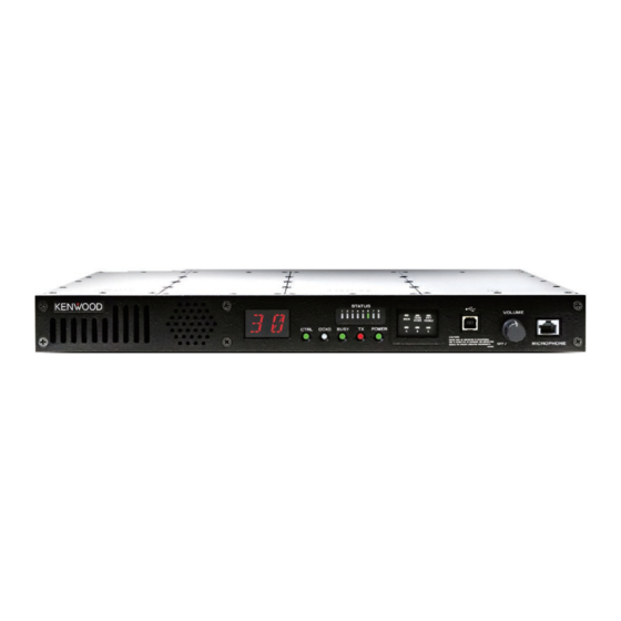
TEST/SPKR
CONTROL I/O
COPYRIGHT © 2015 JVC KENWOOD Corporation
1 2
CTRL
OCXO BUSY
REF OUT
SYNC
LAN
1
2
TABLE OF CONTENTS
STATUS
3 4 5 6 7 8
MON TAKE
RPT
OVER
DISABLE
TX
POWER
A
B
C
FUSE
DC 13.6V
REF IN
This product uses Lead Free solder.
VOLUME
MICROPHONE
OFF/
TX
No.RA033<Rev.001>
2015/12
Advertisement

Related Manuals for Kenwood NXR-5700


Summary of Contents for Kenwood NXR-5700
-
Page 1: Table Of Contents
CONTROL I/O SYNC COPYRIGHT © 2015 JVC KENWOOD Corporation TABLE OF CONTENTS PRECAUTION............... . . 1-4 SPECIFIC SERVICE INSTRUCTIONS . - Page 2 Neither is any liability assumed for damages resulting from the use of the information contained herein. JVC KENWOOD Corporation reserves the right to make changes to any products herein at any time for improvement purposes. Firmware Copyrights The title to and ownership of copyrights for firmware embedded in KENWOOD product memories are reserved for JVC KENWOOD Corporation.
- Page 3 *25 and 30 kHz are not included in the models sold in the USA or US territories. Measurements made per CAI measurement procedures (digital) and TIA-603 (analog); specification are typical. JVC KENWOOD Corporation reserves the right to change specifications without prior notice or obligation. (No.RA033<Rev.001>)1-3...
-
Page 4: Precaution
• The data stored in the personal computer must match the This feature is included in the FPU. model type, when it is written into the flash memory. • Change the NXR-5700 to PC mode, then attach the USB (A- Firmware program- Use when changing the firmware B Type) cable. - Page 5 (KFL.exe). • While "--" is displayed on the LED, the PC and NXR-5700 The data can be input to or read from NXR-5700 and edited on can't communicate. the screen. The programmed or edited data can be printed out.
- Page 6 • “E5” is displayed when IP address configuration is error. • All segments ON • “E6” is displayed when a Frame pulse error is detected. • “E7” is displayed when a transmission is stopped by high tem- perature. • “E8” is displayed when the Failure channel input is activated. •...
- Page 7 Crimp termial Fig.1 2.4.2 External Speaker (KES-5) Barbs The NXR-5700 has a internal built-in speaker, and the external speaker output from the TEST/SPKR connector (15-pin) on the Crimp termial rear of the radio is 3W/4Ω. Use external speaker KES-5. 2.4.2.1 Connection for the KES-5 With the NXR-5700 Fig.2-2...
- Page 8 2.4.3 How to Attach the Supplied Accessories (1) Attach the front glass to the front panel with the supplied screw. <1> (2) To attach the handles on the both sides of the chassis, re- fer to illustration. <2> <2> Handle Front glass <1>...
- Page 9 2.5.2 Adding the RSSI or Reset Terminal on the D-sub 25-pin Connector The configuration for pin 1 of the D-Sub 25-pin connector can be changed to allow it to supply the power source for RSSI. Follow the procedure shown below to change the configuration. Case 1: Add the RSSI.
- Page 10 CIRCUIT DESCRIPTION 2.6.1 Outline The NXR-5700 is a VHF repeater operating in the 136~174MHz frequency range. Transmit RF power range is 0.5W to 25W adjust- able. Receiver's frontend BPFs are electrically adjusted in the factory. 2.6.2 Transmitter unit The transmitter unit (XC1-065 A/3) consists of the following circuit.
- Page 11 REF_IN Q514 Q508 Q504 Q503 IC505 BUFF PLL IC Q507 D501,D502, IC601 IC402 D601,D602 REF_OUT D608,D609, Q609 Q606 Q605 D610,D611 OCXO D603,D604, D605,D606 Q602 1/ 2 IC608 IC607 IC605 X601 IC604 IC602 Fig.2 Internal/external reference circuit 2.6.2.3 Internal frequency reference 19.2MHz PLL circuit The internal frequency reference 19.2MHz PLL circuit produces a reference frequency signal for the transmitter modulation 16.8MHz PLL circuit, the Receiver unit (XC1-066) Receiver PLL circuit and the Control Unit (XC1-064) PLL circuit for ASIC and DSP clock.
- Page 12 2.6.2.4 Transmitter modulation 16.8MHz PLL circuit The transmitter modulation 16.8MHz PLL circuit produces the reference frequency signal for the Transmitter main PLL. The circuit consists of Q301, Q302, Q303, Q304, Q305, X301, IC301, IC302 and IC303. 19.2MHz reference signal is amplified by Q402 and is fed to IC301 as a PLL reference signal. VCXO of X301 generates 16.8MHz signal.
- Page 13 2.6.2.6 Driver circuit The driver circuit amplifies the transmitter frequency signal to the level required for input to the Final Unit (XC3-015 A/5). This circuit consists of RF amplifiers Q201, Q202 and Q204, switches Q203, Q207 and Q208, and operating amplifier IC201. DC switches Q207 and Q208 turn the power supply voltage of RF amplifiers Q201, Q202, and Q204 on and off.
- Page 14 2.6.2.9 Other circuits IC810 is an EEPROM. IC810 keeps TX unit adjustment data. IC811 is a temperature sensor. This temperature sensor is placed near 20MHz VCTCXO (X601), and measures the temperature of VCTCXO. IC801 is an electronic volume control IC for TX and Final unit control. IC802 is an I/O expander for TX and Final unit control.
- Page 15 2.6.3.6 FAN action control circuit MPU controls start and the stop of FAN using the control terminal of the 10V regulator IC. The rotary speed of FAN is controlled with PWM generated in IC802 of the TX unit. To detect a rotary trouble of FAN, MPU watches the output of the circuit detecting a pulse output with the turn of the rotor. MPU controls on/off/speed of FAN according to the temperature information by IC501.
- Page 16 2.6.4.2 1st-Mixer circuit The filtered signal from the front-end circuit is heterodyned with the first local oscillator signal from the PLL frequency synthesizer cir- cuit at the first mixer (IC403) to become a 58.05 MHz first intermediate frequency (IF) signal. Mixer IC403 136~174MHz...
- Page 17 2.6.4.4 2nd-IF circuits Filtered first IF signal is amplified by the IF amplifier (Q605) and then applied to the IF system IC (IC601). IF system IC provides a second mixer, AGC amplifier, and RSSI (Received Signal Strength Indicator). The second mixer mixes the first IF signal with the 57.6 MHz of second local oscillator output and produces the second IF signal of 450 kHz.
- Page 18 2.6.4.5 Receiver PLL circuits The receiver unit (XC1-066) has the PLL circuit for controlling the VCO that generates the hetero signal to the first local oscillator. The first local circuit consists of the VCO (Q205, Q206 and Q207) the Buffer amplifier (Q201 and Q202),the RF amplifiers (Q215), the PLL-IC (IC203), the Passive loop filters (C307, C298, R279, R277and C290) and the Band switches (Q203, Q204, Q209 ,Q210 and Q211).
- Page 19 When the power supply is off, it is backed up by an internal secondary lithium battery. Therefore, the saved data is not lost. 2.6.5.3 LAN interface NXR-5700 is equipped with a 100Base-TX or 10BaseT LAN interface. This circuit consists of IC860 and J860. IC860 is a control IC and J860 is LAN Connector.
- Page 20 2.6.5.4 The DSP circuit consists of a DSP (IC150) and processes the base band signal. The DSP operates on an external clock of 18.432MHz (the same as the IC50), the I/O section operates at 3.3V and the core section operates at 1.6V. The DSP carries out the following processes: Digital Processing •...
- Page 21 2.6.5.6 USB interface NXR-5700 is equipped with a USB device function and supported USB2.0 at full speed. This circuit consists of IC901 and J800. IC901 is a MPU IC that contains the USB controller function. J800 is a USB-B connector on the front panel.
- Page 22 2.6.5.7 Power Supply and Reset Circuit +B voltage is connected DC/DC converter IC (IC1), DC/DC converter IC (IC704), Voltage regulator IC (IC700), AMP switch (Q906) through the fuse (F530). IC1 regulates +B voltage to 5V (50M). PWRGD output of IC1 turns on the IC3, IC4, IC5, IC6 and IC10. And, 50M provides the power to the panel unit LEDs and IC3, IC4, IC5, IC6 and IC10.
- Page 23 Q906 F530 Audio_Amp Q530 IC1 5V PWRGD DC/DC converter AMP_SW IC530 IC10 3.3V Voltage regulator IC906 /OVRB Voltage detector IC3 3.3V Q908 Voltage regulator /OVRB2 /BINT Voltage detector IC4 3.3V Voltage regulator IC6 1.6V /RST Voltage regulator /RST Voltage detector IC5 1.5V Voltage regulator Q706...
- Page 24 2.6.5.9 Temperature sensor The temperature sensor (IC9) monitors temperature around CONTROL-UNIT. The temperature is recorded for the NOR-FLASH memory (IC790). 2.6.5.10 Squelch circuit The squelch circuit amplifies the demodulated noise signal from IC150 after filtering through the BPF circuit. The processed digital noise signal is applied to CODEC IC452, and is converted from digital to analog. The amplified signal is then converted to a DC signal by the detection circuit.
- Page 25 • Modulation circuit (Analog/Digital signal processing) In the case of the Analog Signal Processing mode, the transmitting audio signal is amplified by IC252, input to the TX_MIC terminal of the MPU (IC200), and audio processed by DSP (IC150). The processed audio signal from the MOD terminal of IC200 is passed through an anti-aliasing filter at IC250, and is then amplified to a sufficient level by IC250, and amplified by the summing (TD) amplifier.
- Page 26 Ref. No. Part Name Description Ref. No. Part Name Description Q550, 551 Switching IC532 Analog switch Schottky diode Detector IC533 Power amplifier Zener diode Voltage limiting IC700, 701 Voltage regulator Zener diode Voltage limiting IC702, 703 AND gate D9, 10 Schottky diode Detector IC704 DC/DC converter...
- Page 27 Ref. No. Part Name Description Ref. No. Part Name Description D352 Diode Surge protector IC807~809 D353 Zener Diode Surge protector IC810 E2PROM D354 Diode Surge protector IC811 Temperature sensor D355 Zener Diode Surge protector IC812, 813 D356 Varistor Curennt protector IC901~903 BUS buffer D450, 451...
- Page 28 Ref. No. Part Name Description Ref. No. Part Name Description Q810 Switching IC12 D/A Converter Q811 Transistor Switching IC13 BUS buffer Q901 Switching IC14 I/O expander Q902 Transistor Switching IC15 BUS buffer Q903 Switching IC201, 202 DC amplifier Q904, 905 Transistor Switching IC203...
- Page 29 Ref. No. Part Name Description Name Function D605~612 Diode Limit the RF input power I2CCK I2C clock D613~616 Diode Switching 3.3V power supply D701, 702 Diode Limit the IF power I2CDA I/O I2C data TERMINAL FUNCTION /EWP EEPROM write control signal 2.8.1 Final Unit (XC3-0150-10) (A/5) Ground Name...
- Page 30 2.8.3 Final Unit (XC3-0150-10) (D/5) Name Function Name Function I2CDA I/O I2C data CN800 (To Control Unit XC1-064 CN830) Ground VBUS USB VBUS(5V) output I2CCK2 O I2C clock2 I/O USB Data plus Ground I/O USB Data minus I2CDA2 I/O I2C data2 USB Ground /EWP O EEPROM write control signal...
- Page 31 Name Function Name Function I2CCK2 O I2C clock2 Ground /EWP O EEPROM write control signal Hook detection input O 3.3V power supply Ground ASTSW_TX O TX PLL assist control signal /PTT PTT input O 8V power supply control 33MPU O 3.3V power supply TX_CV TX VCO lock voltage VoLUME_iN...
- Page 32 Name Function Name Function EXT_MOND External monitor signal CN601 (To "REF OUT" BNC Receptacle) REF OUT O 10.0MHz reference signal output TXD0_D25 O UART TX data CN602 (To OCXO Unit X42-328 CN2) /EPTT_D25 External PTT OCXO Optional OCXO reference signal input AI1_D25 Programmable function input 1 CN722 (To Control unit XC1-064 CN101)
- Page 33 Name Function Name Function /RF_B_ON O RF +B switch control signal OCXO_VR_E O /OC_VR_EN, Serial data enable sig- nal to potentiometer of OCXO unit - Ground OCXO_ON O Power supply switch for OCXO unit I2CCK2 O I2C clock2 OX_SCLK2 O SPSCLK1, SPI1 clock - Ground OCXO_CUR OC_CURR, Monitor of the voltage...
- Page 34 2.8.8 TX Unit (XC1-0650-10) (C/3) Name Function Name Function VOLUME_IN Volume control for AF signal CN951 (To TX Unit XC1-065 C/3 CN901) 33MPU 3.3V power supply 50MPU 5.0V power supply /PTT PTT signal Ground Ground 33MPU 3.3V power supply Hook detection output /LED_LAT2 Buffered serial port data latch signal Ground...
- Page 35 Name Function Name Function Ground CN405 (To Final Unit XC3-015 A/5 CN19: OPTIONAL) I2CCK I2C clock SWED_RX Switched RX signal from final unit (For simplex operation with single /EVRXCS2 RX EVOL2 chip select signal antenna) /EVRXCS1 RX EVOL chip select signal CN406 (To RX ANT BNC Receptacle) Ground RX_SIGNAL...
- Page 36 2.8.11 USB Connector (USB-Type B) Signal Modifica- Description/ Spec and Condition Unit Note Name Type tion port Type VBUS I Analog USB VBUS(5V) USB peripheral 4.40 5.25 *Note1 input operation *Note2 Analog USB Data *Note1 minus Data Rate (Full-Speed) Mb/s Analog USB Data plus VIH *Note1...
- Page 37 Signal Modifica- Description/ Spec and Condition Unit Note Name Type tion port Type Digital default Auxiliary Output External voltage value 2 Open collec- Allowable current value Auxiliary Output PU resistor 4.7k Vcc=5+/-2% 2 Open collec- VOL(IO=0mA) tor with PU Analog External Speak- Output level Less...
- Page 38 Signal Modifi- Description/ Spec and Condi- Max Unit Note Name Type cation port Type tion Digital Default Programmable Vcc=5+/-2% Function Input 2 /CMOS Input impedance ohm 47kohm PU to Vcc=5+/- Digital Request Voltage Swing +/-9.0 conform to RS232C to Send /RS232C Digital Programmable...
- Page 39 Signal Modifi- Description/ Spec and Condi- Max Unit Note Name Type cation port Type tion BER_D Digital Error VOH(IO=20uA) 47kohm PU to Vcc=5+/- Rate Data VOL(IO=20uA) TX Siganl GND - Digital Programmable Vcc=5+/-2% Function I/O 1 Input impedance ohm 47kohm PU to Vcc=5+/- VOH(IO=-3mA) Vcc - 47kohm PU to Vcc=5+/-...
- Page 40 Signal Modifi- Description/ Spec and Condi- Max Unit Note Name Type cation port Type tion Digital Programmable Vcc=5+/-2% TP_IN Function I/O 6 or Timing Pulse in for simulcast Input impedance ohm 47kohm PU to Vcc=5+/- VOH(IO=-3mA) Vcc - 47kohm PU to Vcc=5+/- VOL(IO=8mA) 2.8.14 SYNC Connector 1 Signal...
-
Page 41: Disassembly
2.8.16 LAN Connector (RJ-45) Signal Modifi- Description/ Spec and Condition Unit Note Name Type cation port Type Analog TX Signal + 100Base-TX conform to IEEE802.3 +Vout@100ohm 0.95 1.05 -Vout@100ohm -1.05 -0.95 Data rate 125.0 Mbps 10Base-TX Vout@100ohm Data rate 10.0 Mbps Output Impedance 100.0... -
Page 42: Adjustment
SECTION 4 ADJUSTMENT Test Equipment Required for Alignment Test Equipment Major Specifications 1. Standard Signal Generator Frequency Range 136 to 174MHz (SSG) Modulation Frequency modulation and external modulation Output 0.1μV to greater than 1mV 2. Power Meter Input Impedance 50Ω Operation Frequency 136 to 174MHz or more Measurement Capability... - Page 43 Flat cable (36-pin) about 256mm (E37-0979-05) Jig for Drive AMP adjustment (E37-1304-05) ANT Jig for BPF adjustment (E30-3418-25) Test Channel Receiver [MHz] Transmit [MHz] 155.050000 155.100000 136.050000 136.100000 173.950000 173.900000 155.000000 155.000000 155.200000 155.200000 155.400000 155.400000 Test Signaling Analog Decode tone Encode tone None None...
- Page 44 • Signaling number 1 is used for link test with voice. • Signaling number 2 is used for TX modulation signal quality test. i.e, TX adjacent channel power, FSK error, Occupied bandwidth, Emission mask, etc. • Signaling number 3 is used for TX deviation test. If the modulation mode is very narrow, the modulation frequency is 600Hz. If the modulation mode is narrow, the modulation frequency is 1200Hz.
- Page 45 f0 +/- 3.85kHz : 6dB max f0 +/- 12.5kHz : more than 28dB Fig.7 Adjustment Points CN20 CN550 CN21 PA CUR CN22 ANT SW RAMP CN23 CN14 PRT PWR CN24 CN19 CN13 PWR LIM CN16 FINAL UNIT (XC3-015) Component side FINAL UNIT (XC3-015) Component side CN638 RX UNIT (XC1-066)
- Page 46 CN601 CN722 CN207 CN203 CN302 RF OUT DRV PWR LVL VCXO MOD CN721 CN724 CN202 CN303 DRV PWR MB CV2 CN102 VCO MOD CN602 CN204 CN403 CN101 CN103 OCXO CN301 REF UL TX UL CN205 TX CV MOD UL TX UNIT (XC1-065) CN401 REF CV Component side...
- Page 47 Measurement Adjustment Item Condition Specifications / Remarks Test- Unit Parts Method Terminal Unit equipment 4. BPF Ad- FPU Test mode Tracking Rear RX ANT RX PC Adjust it to [Low]: Refer to Fig. 1 (Page.1-44) just 1) Adjust Item: [Sensitivity 1] generator CN403 look like the...
- Page 48 Receiver Section Measurement Adjustment Item Condition Specifications / Remarks Test- Unit Parts Method Terminal Unit equipment 1. RD Out- FPU Test mode Rear RX ANT 80mV ±5mV put level 1) Adjust Item: [RD Level (Ana- Adjust log Wide)] AF VM Control Press [Apply] button to store [Analog...
- Page 49 Measurement Adjustment Item Condition Specifications / Remarks Test- Unit Parts Method Terminal Unit equipment 6. Open FPU Test mode Rear RX ANT Write the fixed value"43" Squelch 1) Adjust Item: [Open Squelch Audio ana- Adjust (Analog Narrow)] lyzer [Analog Connect the SSG to the RX Oscillo- Narrow] ANT.
- Page 50 Measurement Adjustment Item Condition Specifications / Remarks Test- Unit Parts Method Terminal Unit equipment 10. RSSI FPU Test mode Rear RX ANT Press [Apply] button to store Refer- 1) Adjust Item: [RSSI Ref (Ana- Audio ana- the adjustment value. ence Ad- log Wide)] lyzer just...
- Page 51 Measurement Adjustment Item Condition Specifications / Remarks Test- Unit Parts Method Terminal Unit equipment 15 .Low FPU Test mode Rear RX ANT Press [Apply] button to store RSSI Ad- 1) Adjust Item: [Low RSSI the adjustment value. just (NXDN Very Narrow)] [NXDN Connect the SSG to the RX Very Nar-...
- Page 52 Measurement Adjustment Item Condition Specifications / Remarks Test- Unit Parts Method Terminal Unit equipment 19. Exter- FPU Test mode Rear RX ANT 3.0V ±0.1V nal RSSI 1) Adjust Item: [EXT RSSI Off- OFFSET set (Analog Wide)] TEST/ Press [Apply] button to store Adjust Connect the SSG to the RX SPKR...
- Page 53 Transmitter Section Measurement Adjustment Specifications / Re- Item Condition Test- marks Unit Parts Method Terminal Unit equipment 1.Drive FPU Test mode Power CN207 16dBm ±0.1dB Power Ad- 1)Adjust Item: [Drive Amplifier Power] Meter just 2) Frequency: [Low], [Low’], [Center], Press [Apply] button to [High’], [High] store the adjustment Press [Transmit] button.
- Page 54 Measurement Adjustment Specifications / Re- Item Condition Test- marks Unit Parts Method Terminal Unit equipment 8. High FPU Test mode Power Rear TX ANT ±0.5W Power 1) Adjust Item: [RF Power Down De- Meter Down De- tection (High)] Press [Apply] button to tection ad- store the adjustment just...
- Page 55 Measurement Adjustment Specifications / Re- Item Condition Test- marks Unit Parts Method Terminal Unit equipment 15.Bal- FPU Test mode Deviation Rear TX ANT 1) Adjust Gain 1.700KHz ±20Hz ance Ad- 1) Adjust Item: [Balance] Connect the meter A to get just Deviation Meter to the TX ANT end Oscillo-...
- Page 56 Measurement Adjustment Specifications / Re- Item Condition Test- marks Unit Parts Method Terminal Unit equipment 17. TD De- FPU Test mode Deviation Rear TX ANT 0.75kHz Devi- ±0.05kHz viation 1) Adjust Item: [TD Deviation (Analog meter ation adjust [An- Wide)] Oscillo- Control I/ Press [Apply] button to...
- Page 57 Measurement Adjustment Specifications / Re- Item Condition Test- marks Unit Parts Method Terminal Unit equipment 21. QT FPU Test mode Deviation Rear TX ANT 0.75kHz Devi- ±0.05kHz Deviation 1) Adjust Item: [QT Deviation (Analog meter ation adjust [An- Wide)] Oscillo- Press [Apply] button to alog Wide] Connect the Deviation Meter to the TX...
- Page 58 Measurement Adjustment Specifications / Re- Item Condition Test- marks Unit Parts Method Terminal Unit equipment 27. Test FPU Test mode Deviation Rear TX ANT 3.0kHz Devia- ±0.05kHz Tone De- 1) Adjust Item: [Test Tone Deviation meter tion viation ad- (Analog Wide)] Connect the Deviation Oscillo- Press [Apply] button to just...
- Page 59 Measurement Adjustment Specifications / Re- Item Condition Test- marks Unit Parts Method Terminal Unit equipment 33. Re- FPU Test mode Deviation Rear TX ANT 1.0kHz Devia- ±0.05kHz peat Gain 1) Adjust Item: [Repeat Gain (Analog meter tion adjust [An- Wide)] Oscillo- RX ANT Press [Apply] button to...
- Page 60 To adjust the KXK-3(M3) OCXO unit, some preparations are required. (1) The NXR-5700 with the KXK-3(M3) OCXO unit must be warmed up at least 72 hours before the adjustment is made. The envi- ronment temperature must be stable. (2) The frequency counter (or reference oscillator) must be warmed up as defined by the equipment manufacturer.
-
Page 61: Troubleshooting
SECTION 5 TROUBLESHOOTING Fault diagnosis of the BGA(Ball Grid Array) IC Overview: A fiowchart for determining whethe or not the transceiver can't be powered on (the Display does not function) due to broken BGA parts. BGA parts MPU(IC200) DSP(IC150) FLASH_No.1(IC390) FLASH_No.2(IC391) SRAM(IC392) MPU(IC901) - Page 62 When a normal value is confirmed. Checking the output signal output from the MPU(IC200) When an abnormal via software control. value is confirmed. Remove R716,Q710 and Q707 . If the MPU(IC200)side Normal voltage Points to be checked is 0V, the MPU(IC200) or FALSH or SRAM or DSP may 3.3V A8oN R716 be broken.
- Page 63 MPU(IC901) and DDR3 (IC791) Troubleshooting Overview : The flowchart about troubleshooting of BGA package MPU (IC901) and DDR3 (IC791) . This flowchart describe about "error display of e7" that is meant an error occurrence when the MPU (IC901) communicate to other MPU (IC200).
- Page 64 5.2.2 Detail of MPU (901) and DDR3 (IC791) troubleshooting Note It might not check capacitor, because it is unlikely the "Monolithic Ceramic Capacitors" become short circuit Gray cell and in parenthesis are capacitor check The display indicates IC700 33BU output 3.3V Check input(L701) and around “e7”...
- Page 65 From A IC703 OUTY(R725) output Check IC703's input of R714 IC703 INA and INB input 3.3V. 3.3V. and R715. Failure of R912 or IC703 are doubted. PWRONRSTn High : OK X901 oscillate 24MHz(R903 or Check around X901 R904) Main Clock 24MHz : OK Checking the System Boot Mode.
- Page 66 For the XC1-064, a UPC code and UPC barcode is not printed FPU Data NXR-5700 K type data. on the KENWOOD ESN Label. If necessary, cut the label at (PC programming mode) the cut-off line and attach only the serial number.
- Page 67 SCHEMATIC DIAGRAM FINAL UNIT (XC3-0150-10) AMPLIFIER IC10 RA60H1317M1A T H:25W M:5W XC3-015 A/5 L:0.5W R :0W PA UNIT T H:3.9V T H:13.0V SURGE M:3.6V M:13.3V ABSORBER L:3.6V L:13.4V T:40mW(+16dBm) C122 R125 R :0V CN25 R :13.5V TX ANT R:0W D11,D16 1000p SWITCHING 3DB ATT...
- Page 68 CONTROL UNIT (1/2) (XC1-0640-10) RX UNIT TX UNIT XC1-066 XC1-065 A/3 5.0V CN722 IC1,D1 3.3V DC-DC 5.0V CONVERTER BU33TD2WNVX VOLTAGE $CN2 REGULATOR VOLTAGE 0.1u 6.8u 13.6V STBY DETECTOR VOLTAGE CN101 BOOT REGULATOR BD5329FVE IC10 BU33TD2WNVX VIN VoUT CoMP STBY SS/TR C100 100p C120...
- Page 69 CONTROL UNIT (2/2) (XC1-0640-10) 1.1V(Standby Mode) IC704,D704 C776 DC-DC L768 VDD_MPU CONVERTER 3.8V [1608] L706 4.7u L708 C725 $CN705 13.6V 0.1u REVERSE D865 CURRENT BOOT DA2S101 PROTECTOR L702 CoMP Q708 SS/TR VOLTAGE REGULATOR VSENSE GND1 RT/CLK PWRGD 36 35 34 33 32 31 30 29 28 27 26 25 Q707 GND2 3.3V...
- Page 70 TX UNIT (XC1-0650-10) TX UNIT XC1-065 A/3 RIPPLE FILTER CN108 CN112 CN117 Q102 7.2V CN105 CN110 CN115 CN119 R201 R201 R:0V R110 DSC90010(S) 80C_1 T:7.8V SWITCHING VCO A:7.0V R221 80C_2 R116 VCO B:0V Q105 EM6M2 R150 GND SPRING CN109 CN113 CN118 R129 CN206...
- Page 71 RX UNIT (XC1-0660-10) Q404 DC AMP L431 SSM3J334R 50RF_1 R901 R901 IC405 BU7261G R476 100k R494 R468 R470 680k 3.9k R477 RX ANT CN403 100k CN405 E04-0491-05 C480 100p E04-0193-05 D404-409 L406 L411 D470-473 D464-469 D458-463 D410-415 454-457 D422-427,444-453 TUNING D428-443 TUNING TUNING...
- Page 72 INTERCONNECTION DIAGRAM TEST/SPKR (REAR PANEL ViEW) CONTROL I/O (REAR PANEL VIEW) FINAL UNIT XC3-015 E/5 CN903 CN905 C N 9 0 1 VOLUME_IN VOLUME_IN CN951 RSSI 50MPU TX UNIT 50MPU 33MPU 33MPU XC1-065 C/3 TX UNIT J901 XC1-065 B/3 33MPU 33MPU /LED_LAT2 /LED_LAT2...
- Page 73 PRINTED CIRCUIT BOARD FINAL UNIT (XC3-0150-10) --- Component side view (J7C-0103-00) --- IC500 J7C-0103 R561 C560 IC500 R650 R508 IC501 D801 R560 C561 R651 Q550 Q551 R652 D802 R502 L500 R562 IC501 R653 XC3-015 D550 J7C-0103-00 IC400 RAMP_TX IC401 C410 R464 R401 R457...
- Page 74 FINAL UNIT (XC3-0150-10) --- Foil side view (J7C-0103-00) --- C554 R550 L800 L801 R102 R121 C106 R105 R103 C456 C360 C109 C908 L900 C902 C914 (No.RA033<Rev.001>) 2-8 2-8 (No.RA033<Rev.001>)
- Page 75 A-1C ADDRESS TABLE OF BOARD PARTS Side Y axis Each address may have an address error by one X axis interval. REF.NO. LOCATION REF.NO. LOCATION REF.NO. LOCATION REF.NO. LOCATION REF.NO. LOCATION REF.NO. LOCATION REF.NO. LOCATION REF.NO. LOCATION REF.NO. LOCATION REF.NO. LOCATION REF.NO. LOCATION REF.NO. LOCATION REF.NO. LOCATION A- 5C A- 5D A- 3C...
- Page 76 CONTROL UNIT (XC1-0640-10) --- Component side view (J7C-0100-00) --- RSSI CN100 CN342 CN555 C359 R355 R435 Q410 C418 C419 CN343 R413 R437 IC533 R425 L348 R415 C421 C537 C417 R538 C535 R540 C536 CN706 C531 J7C-0100-00 C538 IC250 R533 CN410 C300 R268 C393...
- Page 77 CONTROL UNIT (XC1-0640-10) --- Foil side view (J7C-0100-00) --- C581 C579 R596 R594 C355 R561 R595 R593 IC503 Q343 C509 C503 C542 R502 Q342 Q340 R507 C505 C506 C504 D550 D555 D557 D559 D560 D561 D562 IC390 IC391 Q341 Q344 F530 C507 R391...
- Page 78 A-1C ADDRESS TABLE OF BOARD PARTS Side Y axis Each address may have an address error by one X axis interval. REF.NO. LOCATION REF.NO. LOCATION REF.NO. LOCATION REF.NO. LOCATION REF.NO. LOCATION REF.NO. LOCATION REF.NO. LOCATION REF.NO. LOCATION REF.NO. LOCATION REF.NO. LOCATION REF.NO. LOCATION REF.NO. LOCATION REF.NO. LOCATION REF.NO. LOCATION REF.NO. LOCATION REF.NO. LOCATION REF.NO. LOCATION Q534 A- 4B A- 3A...
- Page 79 TX UNIT (XC1-0650-10) --- Component side view (J7C-0101-10) --- Q610 CN302 R763 R245 R242 R239 R832 R229 R833 R819 C225 C226 R816 R244 R230 R233 R226 CN102 TH201 R231 L801 R228 C801 CN202 C802 C831 R802 TX_CV R807 C830 R804 C829 R805 IC727...
- Page 80 TX UNIT (XC1-0650-10) --- Foil side view (J7C-0101-10) --- C642 Q608 IC603 R650 R674 Q607 R660 C648 C248 R787 R659 Q803 C232 C233 C637 R651 IC728 C804 R812 R785 C796 IC728 L606 R810 R815 R327 C695 C624 C321 R348 D613 C234 C326 L208...
- Page 81 A-1C ADDRESS TABLE OF BOARD PARTS Side Y axis Each address may have an address error by one X axis interval. REF.NO. LOCATION REF.NO. LOCATION REF.NO. LOCATION REF.NO. LOCATION REF.NO. LOCATION REF.NO. LOCATION REF.NO. LOCATION REF.NO. LOCATION REF.NO. LOCATION REF.NO. LOCATION REF.NO. LOCATION REF.NO. LOCATION REF.NO. LOCATION REF.NO. LOCATION REF.NO. LOCATION REF.NO. LOCATION REF.NO. LOCATION Q501 B- 2C D613...
- Page 82 RX UNIT (XC1-0660-10) --- Component side view (J7C-0102-00) --- CN638 TC606 XF604 C603 L418 L603 R456 R460 R605 XF602 C517 NARROW C460 C731 C470 TC604 IC404 TC602 C482 R602 R516 TC608 R475 C601 C604 C465 C463 R505 R494 L601 C474 TC605 C476 XF603...
- Page 83 RX UNIT (XC1-0660-10) --- Foil side view (J7C-0102-00) --- R660 L627 C672 L632 R634 R639 L427 L642 C631 L441 L415 C625 D444 C503 C627 R669 L421 R641 C471 C630 Q602 R479 D427 D424 D616 R694 C454 D411 D410 D612 C486 D426 D425 D610 C673...
- Page 84 A-1C ADDRESS TABLE OF BOARD PARTS Side Y axis Each address may have an address error by one X axis interval. REF.NO. LOCATION REF.NO. LOCATION REF.NO. LOCATION REF.NO. LOCATION REF.NO. LOCATION REF.NO. LOCATION REF.NO. LOCATION REF.NO. LOCATION REF.NO. LOCATION REF.NO. LOCATION REF.NO. LOCATION REF.NO. LOCATION REF.NO. LOCATION REF.NO. LOCATION REF.NO. LOCATION REF.NO. LOCATION Q803 B- 5A D459...
- Page 85 BLOCK DIAGRAM FINAL UNIT FINAL UNIT (XC3-015) IC10 TX IN RA60H1317M1A D11,D16 CN25 L8103R FROM COUPLER TX UNIT TX ANT D10,D22 CN207 LTC6101BIS5-F D1,D9 RB731U RB731U D14,D15,D19.D20 IC250 CN19 JDP2S12CR IC450 NJG1615HA8 LM56BIMM/NOPB BA2904FVM 2V ref TEMP SSM3K15AMFV Q4,Q5 RX ANT SENS 2SJ506-E(S) BA2904FVM...
- Page 86 CONTROL UNIT CONTROL UNIT (XC1-064) Connector +B(13.6V) +B(13.6V) E41-2673-05 A8RST RESET from DSUB25 (Option) A8ON PMIC 38M DCDC IC750 IC704 50MPUDCDC TPS65910A3A1R TPS54240DGQ VDD_MPU TPS54240DGQ 33_USB Q708 LTC014EEBFS8 LTC014EEBFS8 Q707 VDDA_ADC PWRGD LTC014EEBFS8 HWV Resistor 18VDDS_2 18VDDS 33D LDO 33MPULDO IC701 18_USB BD33KA5WF...
- Page 87 TX UNIT TX UNIT (XC1-065) Q102 DSC90010(S) FWD PWR CN723 Ripple FWD_PWR (ADC) E40-6656-05 Q105 REV PWR REV_PWR (ADC) EM6M2 VCO_A/B PA CUR Q101 80C2 VCO-A PA_CUR (ADC) DSC90010(S) Ripple Q107 CAP_TEMP 200C Q207 SSM3K15AMFV MCH3914-H/8/ CAP_TEMP (ADC) Q208 SSM3J334R CN207 Q722 E04-0193-05...
- Page 88 RX UNIT RX UNIT (XC1-066) RF_B_ON RSSI_OFFSET VSET IF_GAIN_ADJ EXT_RSSI MIX_STAT DMR_SW N/NV RX_CV REF_EXIST VCO_A LNA_CUR RX_UL VCO_B RX_VER0 VCO_C DETO RX_VER1 VCO_D RSSI RSSI_GAIN0 RSSI_GAIN1 RX_UL ASTSW_RX RXASSIST LNA_ON /EWP I2CDA2 I2CCK2 I2CDA I2CCK /EVRXCS2 /EVRXCS1 /RXPCS /RXIOINT /IO_RST 33MPU RF_B_ON...
- Page 89 PARTS LIST [NXR-5700] * SAFETY PRECAUTION Parts identified by the symbol are critical for safety. Replace only with specified part numbers. * BEWARE OF BOGUS PARTS Parts that do not meet specifications may cause trouble in regard to safety and performance.
- Page 90 Exploded view of general assembly and parts list Block No.M1MM EXCITER FINAL CONTROL IC11 IC550 IC813 IC10 IC812 FINAL UNIT<04> IC533 TX UNIT<02> CONTROL UNIT<01> 19 30 RX UNIT<03> 3-2(No.RA033<Rev.001>)
- Page 91 B11-1842-04 FILTER 17SEG B1B-0056-00 FILTER PF KEY B1B-0058-00 FILTER B1B-0059-00 FILTER STATUS B42-7417-04 STICKER NEXEDGE B4D-0030-00 BADGE KENWOOD E0E-0023-00 C.RECEPTACLE-BN E30-7583-05 TRUNK CABLE TX-FINAL E3A-0149-00 ANTENNA CABLE RX/REF IN/REF OUT(x3) E3A-0176-00 DC CORD E3F-0080-00 FLAT CABLE DISP-CONT E3F-0081-00 FLAT CABLE...
- Page 92 Electrical parts list CONTROL UNIT Symbol No. Part No. Part Name Description Local XC1-0640-10 LTC014EEBFS8 DIGI TRANSISTOR *Note : This part cannot be replaced. There- SSM3K15AMFV SSM3K15AMFV fore, this part is not supplied as a service part. LSCR523EBFS8 TRANSISTOR LSAR523EBFS8 TRANSISTOR Block No.
- Page 93 Symbol No. Part No. Part Name Description Local Symbol No. Part No. Part Name Description Local D864 LXES15AAA1133 VARISTOR CK73HB1H103K C CAPACITOR 10000pF 50V K D865 DA2S101 DIODE CC73HCH1H121J C CAPACITOR 120pF 50V J D866 LXES15AAA1133 VARISTOR CC73HCH1H470J C CAPACITOR 47pF 50V J D867 LXES15AAA1133 VARISTOR...
- Page 94 Symbol No. Part No. Part Name Description Local Symbol No. Part No. Part Name Description Local C210 CC73HCH1H020C C CAPACITOR 2pF 50V C C313 CC73HCH1H101J C CAPACITOR 100pF 50V J C211 CC73HCH1H101J C CAPACITOR 100pF 50V J C316 CK73HBB1H102K C CAPACITOR 1000pF 50V K C212...
- Page 95 Symbol No. Part No. Part Name Description Local Symbol No. Part No. Part Name Description Local C503 CK73GBB1C104K C CAPACITOR 0.1uF 16V K C715 CK73HB1H103K C CAPACITOR 10000pF 50V K C504 CK73GBB1C104K C CAPACITOR 0.1uF 16V K C716 CK73HB1H103K C CAPACITOR 10000pF 50V K...
- Page 96 Symbol No. Part No. Part Name Description Local Symbol No. Part No. Part Name Description Local C876 CK73GXR0J475K C CAPACITOR 4.7uF 6.3V K C980 CK73HBB1A104K C CAPACITOR 0.1uF 10V K C879 CK73HB1A105K C CAPACITOR 1uF 10V K C981 CK73HBB1A104K C CAPACITOR 0.1uF 10V K C880...
- Page 97 Symbol No. Part No. Part Name Description Local Symbol No. Part No. Part Name Description Local RK73HB1J562J MG RESISTOR 5.6kΩ 1/16W J R175 RK73HB1J220J MG RESISTOR 22Ω 1/16W J RK73HB1J472J MG RESISTOR 4.7kΩ 1/16W J R176 RK73HB1J473J MG RESISTOR 47kΩ...
- Page 98 Symbol No. Part No. Part Name Description Local Symbol No. Part No. Part Name Description Local R284 RK73HB1J104J MG RESISTOR 100kΩ 1/16W J R430 RK73HB1J101J MG RESISTOR 100Ω 1/16W J R285 RK73HB1J104J MG RESISTOR 100kΩ 1/16W J R431 RK73HB1J473J MG RESISTOR 47kΩ...
- Page 99 Symbol No. Part No. Part Name Description Local Symbol No. Part No. Part Name Description Local R560 RK73HB1J473J MG RESISTOR 47kΩ 1/16W J R765 RK73HB1J103J MG RESISTOR 10kΩ 1/16W J R561 RK73HB1J473J MG RESISTOR 47kΩ 1/16W J R766 RK73HB1J000J MG RESISTOR 0Ω...
- Page 100 Symbol No. Part No. Part Name Description Local Symbol No. Part No. Part Name Description Local R918 RK73HB1J000J MG RESISTOR 0Ω 1/16W J LR79Z0GU6R8M CHIP INDUCTOR R919 RK73HB1J000J MG RESISTOR 0Ω 1/16W J LB73G0AM-004 CHIP FERRITE R920 RK73HB1J000J MG RESISTOR 0Ω...
- Page 101 Symbol No. Part No. Part Name Description Local Symbol No. Part No. Part Name Description Local L864 L33-3033-05 CHOKE COIL IC604 NJU6368PF1 L865 LB73G0AM-004 CHIP FERRITE IC605 BU7261G L866 L92-0621-15 CHIP FERRITE IC606 BA2904FVM L867 L92-0621-15 CHIP FERRITE IC607 AD5312BRM L868...
- Page 102 Symbol No. Part No. Part Name Description Local Symbol No. Part No. Part Name Description Local Q510 LSCR523EBFS8 TRANSISTOR D614 DZ2J030(M) ZENER DIODE Q511 SSM3K15AMFV D615 CSA70-401L SURGE ABSORBER Q512 SSM3K15AMFV D801 DB2J40700 DIODE Q513 SSM3K15AMFV D901 SML-D12V8WPQ Q514 SSM3K15AMFV D902...
- Page 103 Symbol No. Part No. Part Name Description Local Symbol No. Part No. Part Name Description Local C160 CC73GCH1H150G C CAPACITOR 15pF 50V G C314 CC73GCH1H181J C CAPACITOR 180pF 50V J C161 CC73GCH1H330J C CAPACITOR 33pF 50V J C315 CC73GCH1H470J C CAPACITOR 47pF 50V J C162...
- Page 104 Symbol No. Part No. Part Name Description Local Symbol No. Part No. Part Name Description Local C462 CK73GBB1H103K C CAPACITOR 0.01uF 50V K C566 CK73GB1H104K C CAPACITOR 0.1uF 50V K C463 CK73GBB1H103K C CAPACITOR 0.01uF 50V K C567 CK73GBB1H103K C CAPACITOR 0.01uF 50V K C464...
- Page 105 Symbol No. Part No. Part Name Description Local Symbol No. Part No. Part Name Description Local C673 CK73GBB1H102K C CAPACITOR 1000pF 50V K C873 CK73GBB1H103K C CAPACITOR 0.01uF 50V K C674 CK73GB1H104K C CAPACITOR 0.1uF 50V K C874 CK73GBB1H103K C CAPACITOR 0.01uF 50V K C675...
- Page 106 Symbol No. Part No. Part Name Description Local Symbol No. Part No. Part Name Description Local R136 RK73GB2A474J MG RESISTOR 470kΩ 1/10W J R242 RK73GB2A000J MG RESISTOR 0Ω 1/10W J R138 RK73GB2A000J MG RESISTOR 0Ω 1/10W J R244 RK73GB2A000J MG RESISTOR 0Ω...
- Page 107 Symbol No. Part No. Part Name Description Local Symbol No. Part No. Part Name Description Local R431 RK73GB2A105J MG RESISTOR 1MΩ 1/10W J R552 RK73GB2A563J MG RESISTOR 56kΩ 1/10W J R432 RK73GB2A000J MG RESISTOR 0Ω 1/10W J R553 RK73GB2A000J MG RESISTOR 0Ω...
- Page 108 Symbol No. Part No. Part Name Description Local Symbol No. Part No. Part Name Description Local R654 RK73GB2A100J MG RESISTOR 10Ω 1/10W J R758 RK73GB2A000J MG RESISTOR 0Ω 1/10W J R656 RK73GB2A333J MG RESISTOR 33kΩ 1/10W J R759 RK73GB2A103J MG RESISTOR 10kΩ...
- Page 109 Symbol No. Part No. Part Name Description Local Symbol No. Part No. Part Name Description Local R866 RK73GB2A100J MG RESISTOR 10Ω 1/10W J L115 L41-1005-33 CHIP INDUCTOR R867 RK73GB2A000J MG RESISTOR 0Ω 1/10W J L116 LB73G0BA-004 CHIP FERRITE R872 RK73GB2A000J MG RESISTOR...
- Page 110 Symbol No. Part No. Part Name Description Local Symbol No. Part No. Part Name Description Local L615 L41-6885-33 CHIP INDUCTOR IC201 BU7261G L616 L41-5685-33 CHIP INDUCTOR IC202 BA2904FVM L721 LB73G0BA-004 CHIP FERRITE IC203 SKY72310362LF L722 LB73G0BA-004 CHIP FERRITE IC402 BA2904FVM L801...
- Page 111 Symbol No. Part No. Part Name Description Local Symbol No. Part No. Part Name Description Local D404 BB664-02V VARI CAP DIODE D613 RN142S DIODE D405 BB664-02V VARI CAP DIODE D614 RN142S DIODE D406 BB664-02V VARI CAP DIODE D615 RN142S DIODE D407...
- Page 112 Symbol No. Part No. Part Name Description Local Symbol No. Part No. Part Name Description Local C226 CC73GCH1H150G C CAPACITOR 15pF 50V G C409 CK73GBB1H102K C CAPACITOR 1000pF 50V K C227 CC73GCH1H120G C CAPACITOR 12pF 50V G C410 CK73GBB1H102K C CAPACITOR 1000pF 50V K C228...
- Page 113 Symbol No. Part No. Part Name Description Local Symbol No. Part No. Part Name Description Local C512 CK73GBB1H102K C CAPACITOR 1000pF 50V K C676 CK73GB1H104K C CAPACITOR 0.1uF 50V K C514 CC73GCH1H030B C CAPACITOR 3pF 50V B C677 CK73GB1H104K C CAPACITOR 0.1uF 50V K...
- Page 114 Symbol No. Part No. Part Name Description Local Symbol No. Part No. Part Name Description Local TC604 C05-0611-05 TRIM CAPACITOR R233 RK73GB2A474J MG RESISTOR 470kΩ 1/10W J TC605 C05-0611-05 TRIM CAPACITOR R234 RN73GE1J680D MF RESISTOR 68Ω 0.063W D TC606 C05-0611-05 TRIM CAPACITOR...
- Page 115 Symbol No. Part No. Part Name Description Local Symbol No. Part No. Part Name Description Local R451 RK73GB2A104J MG RESISTOR 100kΩ 1/10W J R608 RK73GB2A272J MG RESISTOR 2.7kΩ 1/10W J R452 RK73GB2A104J MG RESISTOR 100kΩ 1/10W J R611 RK73GB2A000J MG RESISTOR 0Ω...
- Page 116 Symbol No. Part No. Part Name Description Local Symbol No. Part No. Part Name Description Local R730 RK73GB2A152J MG RESISTOR 1.5kΩ 1/10W J L205 LB73G0AM-004 CHIP FERRITE R731 RK73GB2A152J MG RESISTOR 1.5kΩ 1/10W J L206 L41-8278-08 CHIP INDUCTOR R732 RK73GB2A102J MG RESISTOR...
- Page 117 Symbol No. Part No. Part Name Description Local Symbol No. Part No. Part Name Description Local L438 LB73G0AM-004 CHIP FERRITE CN639 E04-0491-05 PIN SOCKET L439 L34-4612-05 AIR CORE COIL CN641 E04-0491-05 PIN SOCKET L440 L41-5688-08 CHIP INDUCTOR CN655 E23-1330-05 TERMINAL L441...
- Page 118 Symbol No. Part No. Part Name Description Local Symbol No. Part No. Part Name Description Local CE32BM1V220M E CAPACITOR 22uF 35V M C453 CK73GBB1H102K C CAPACITOR 1000pF 50V K C92-0905-05 OS-CON 47uF 35V C454 CK73GBB1H102K C CAPACITOR 1000pF 50V K C92-0905-05 OS-CON 47uF 35V...
- Page 119 Symbol No. Part No. Part Name Description Local Symbol No. Part No. Part Name Description Local RK73GB2A000J MG RESISTOR 0Ω 1/10W J R661 RK73GB2A473J MG RESISTOR 47kΩ 1/10W J RK73FB2B120J MG RESISTOR 12Ω 1/8W J R800 RK73GB2A104J MG RESISTOR 100kΩ...
- Page 120 Packing materials and accessories parts list Block No.M2MM Packing and accessories Block No. [M][2][M][M] Symbol No. Part No. Part Name Description Local B10-2781-04 FRONT GLASS Accessary B5A-0713-00 INST.MANUAL E/S/F ------------ PAMPHLET ------------ PAMPHLET CANADA TA ------------ PAMPHLET SOFTWARE E30-3427-45 DC CORD Accessary / DC E3A-0177-00...
- Page 121 MEMO...
- Page 122 JVC KENWOOD Corporation Communications Systems Business Unit (No.RA033<Rev.001>) Printed in Japan...