Table of Contents
Advertisement
Quick Links
This service manual provides a variety of service
information.
It contains the mechanical structure of the CD-RW
Drive and the electronic circuits in schematic form.
This CD-RW Drive was manufactured and
assembled under our strict quality control
standards and meets or exceeds industry
specifications and standards.
This CD-R/RW drive is an internal drive unit
designed for use with IBM PC, HP Vectra, or
1. General
1) Enhanced IDE interface.
2) Internal 5.25 inch, halfheight CD-R/RW Drive.
3) 2 Mbyte buffer memory.
4) Audio CD like tray loading of a disc without using a caddy.
5) Power loading and power eject of a disc. The disc can also be ejected manually.
6) Supports Power saving mode and Sleep mode.
2. Supported disc formats
1) Reads and writes data in each CD-ROM, CD-ROMXA, CD-I FMV, Video CD, and CD-EXTRA
2) Reads data in Photo CD (Single and Multi session).
3) Reads and writes standard CD-DA.
4) Reads and writes CD-R discs conforming to "Orange Book Part 2".
5) Reads and writes CD-RW discs conforming to "Orange Book Parts 3".
3. Supported write method
1) Disc at once (DAO), Session at once (SAO), Track at once (TAO), Variable packet, Fixed packet.
4. Performance
1) Random 120 ms average access time.
2) Max 3,600 kB/sec (Max 24X) Sustained Transfer rate.
3) Supports real time error correction and real time layered error correction at each speeds.
4) Supports CD-R write operation at each standard speed, double speed and quadruple speed.
5) Supports CD-RW write operation at double speed.
6) PIO Mode 4 & Multi DMA Mode 2 Support.
7) MPC-3 Spec compliant.
5. Audio
1) Output 16 bit digital data over ATA interface.
2) 8 fs Oversampling Filter for CD Audio
3) Software Volume Control
4) Equipped with audio line output and headphone jack for audio CD playback.
5) Front panel Volume Control for Headphone Output.
INTRODUCTION
compatible computer. It can write as much as 650
Mbytes of digital data into CD-R/RW disc, and can
read as much as 650 Mbytes of digital data stored
in a CD-ROM, CD-R and CD-RW disc.
The CED-8041B can easily meet the upcoming
MPC level 3 specification, and its Enhanced
Intelligent Device Electronics (E-IDE) and ATAPI
interface allows Plug and play integration in the
majority of today's PCs without the need of an
additional interface card.
FEATURES
3
Advertisement
Table of Contents

Related Manuals for LG CED-8042B


Summary of Contents for LG CED-8042B
- Page 1 INTRODUCTION compatible computer. It can write as much as 650 This service manual provides a variety of service Mbytes of digital data into CD-R/RW disc, and can information. read as much as 650 Mbytes of digital data stored It contains the mechanical structure of the CD-RW in a CD-ROM, CD-R and CD-RW disc.
-
Page 2: Specifications
SPECIFICATIONS 1. SYSTEM REQUIREMENTS -CPU: IBM Compatible Pentium 100MHZ (or faster) (For 4X Write speed, 166MHz or faster recommended.) -16MB Memory or greater 2. SUPPORTING OPERATING SYSTEM • DOS 3.1 or Higher • Solaris Ver 2.4 or higher • Windows 3.1 •... -
Page 3: Power Requirements
* Burst Data Transfer Rate (ATAPI) ........16.67 Mbytes/sec (PIO Mode 4) 16.67 Mbytes/sec (MULTI-DMA Mode 2) 2) Average Access Time Random Access ..............120 ms Typical (Max.24X) : INCLUDING LATENCY 3) Data Buffer Capacity ............2 Mbytes 5. POWER REQUIREMENTS 1) Voltage +5 V DC with + 5% tolerance, less than 90 mVp-p Ripple voltage +12 V DC with + 5% tolerance, less than 90 mVp-p Ripple voltage 2) Current... -
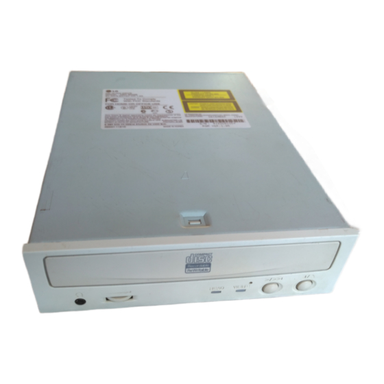
Page 4: Location Of Customer Controls
LOCATION OF CUSTOMER CONTROLS Front Panel Disc Tray Stop/Eject Button Play/Skip Button Volume Control Drive Activity Indicators Headphone Jack 1. Disc tray 4. Volume control This is the tray for the disc. Place the disc on the This is used to adjust the output volume of the ejected disc tray, then lightly push the tray (or headphone jack. -
Page 5: Rear Panel
Rear Panel IDE Interface Connector Analog Audio Output Connector Power Connector Jumper Connector Digital Audio Output Connector 1. Power Connector 3. Jumper Connector Connects to the power supply (5-and 12-V DC) of This jumper determines whether the drive is the host computer. configured as a master or slave. -
Page 6: Major Ic Internal Block Diagram And Pin Description
MAJOR IC INTERNAL BLOCK DIAGRAM AND PIN DESCRIPTION IC601 (AK8563) : Analog Signal Processor LSI for CD-R/RW Block Diagram SRFO HAVC RF_EQUALIZER FOCUS & XTAND TRACK XTOR MPDSH SPPO AGCON GAINUP2 GAINUP3 SPDSH ATIP ATFM SADBC ATFG AGC1C AGC2C RFOM AGC3C WBLSH GAINUP1... -
Page 7: Pin Description
• Pin Description Pin No. Name Pin Description AVDD3 Analog Positive Power Source Pin FPDIN Laser Monitor Diode Contact Pin FVREF Reference Voltage Level Input Pin for APC FPDO Laser Monitor Output (Connect I/V conversion resistor between FPDIN)/ Laser Monitor Voltage Input WREF Power Setting Voltage Input for Write APC VWDC... - Page 8 Pin No. Name Pin Description XRST Register Reset Pin. ”L” Register Initialization WLDON Write LD Control Input. “L” Write APC Setting to Zero, “H” LD ON AGCON Wobble AGC Enable Input. “H” AGC ON, “L” AGC reset TESTAGC Test Pin ATFM Wobble Signal Output AGC1C...
- Page 9 IC202 (HD64F3062) : MICOM Block Diagram Port 3 Port 4 Address bus P5 /A Data bus (upper) P5 /A P5 /A Data bus (lower) P5 /A EXTAL P2 /A XTAL P2 /A STBY H8/300H CPU P2 /A P2 /A RESO/FWE* P2 /A P2 /A Interrupt controller...
- Page 10 •Pin Description Description Port Name Assign CS7/TMO0/TP8/PB0 ACT_MUTE FCS, TPK, and SLD ON/OFF CS6/TMIO1/TP9/PB1 /CSMODE address decoder enable output CS5/TMO2/TP10/PB2 /CS1RL CHIP SELECT1 (Enable to access buffer memories) CS4/TMIO3/TP11/PB3 /CS0RL CHIP SELECT0 (Enable to access internal registers) TP12/PB4 /XRST CXD3011 reset output TP13/PB5 LD_ON Laser diode on/off control output...
- Page 11 Description Port Name Assign A14/P26 /PLAY_KEY Play_key input A15/P27 /EJECT_KEY Eject_key input A16/P50 SENS SENS input A17/P51 MA/SL Master / slave detection input A18/P52 MONIT A19/P53 SQSO Sub-Q 80bit input P60/WAIT SRDY Data ready input P61/BREQ AGCON Wobble AGC enable output P62/BACK SQCK SQSO(Sib-Q 80bit) readout clock...
- Page 12 IC204 (74VHC374MTC) : Expander • Pin Description Description Port Name Assign Output enable input XTSEL CXD3011R-1 crystal selection output Data input Data input ASYMCLR Control output for discharging ASYM1/ASYM2 SPNBOOST spindle gain selection output Data input Data input SPN8/12CM 8/12cm Disc control output Clock input SPNON SPINDLE start / stop control output...
-
Page 13: Digital Out
IC501 (CXD3011 R-1) : CD Digital Signal Processor with Built-in Digital Servo and DAC Block Diagram Asymmetry Correction 84 5 6 51 30 32 28 74 75 76 DAC BLOCK PWMLP MCKO 8Fs Digital Filter PWMLN V16M PWMRP Clock 1 bit DAC VCKI 32K RAM PWMRN... - Page 14 • Pin Description Pin No. Symbol Description Slide Error input Focus Error input Center voltage input VPCO1 1, Z, 0 Output of VCO2 charge pump for vari-pitch EFM PLL VPCO2 1, Z, 0 Output 2 of VCO2 charge pump for vari-pitch EFM PLL ON/OFF switching by Command £§E VCTL Input of VCO2 control voltage for vari-pitch EFM PLL...
- Page 15 Pin No. Symbol Description DA08 1, 0 Outputs DA8 when PSSL=1, or GFS when PSSL=0. DA07 1, 0 Outputs DA7 when PSSL=1, or RFCK when PSSL=0. Digital Power supply DA06 1, 0 Outputs DA6 when PSSL=1, or C2PO when PSSL=0. DA05 1, 0 Outputs DA5 when PSSL=1, or XRAOF when PSSL=0.
- Page 16 Pin No. Symbol Description Analog power supply Power supply for master clock XTLO 1, 0 X'tal oscillation circuit output of master clock. XTLI X'tal oscillation circuit input of master clock. GND for master clock Analog GND PWMLP 1, Z, 0 PWM output for Audio DAC, L channel PWMLN 1, Z, 0...
- Page 17 Pin No. Symbol Description TES2 Test Pin. Normally "L" TES3 Test Pin. Normally "L" PWMI External input of spindle motor Digital power supply VCOO 1, 0 Output of oscillation circuit analog EFM PLL VCOI Input to oscillation circuit for analog EFM PLL. f =8.6436MHz LOCK TEST...
- Page 18 IC209 (RL5E808B) Block Diagram RD[15:0] DEFS Subcode Subcode DSFS ROEB RCAS0B SUBIN Operator RCAS1B:RWE1B SUBCK RWE0B DRAM if RRAS0B Buffer RA11:RRAS1B RA10:RRAS2B Manager LRCKIN RA9:RRAS3B SDIN CD-DA if RA[8:0] BTCK C2PO DASPB CS3FXB CS1FXB CIRC RAM if Encoder DIAGB ATAPI if IOCS16B DINT ESFS...
- Page 19 • Pin Description Clock Pin No. Pin Name Type Description CLKIN CLOCK IN : System Clock VCOIN VCO IN : Input for VCO CPOUT CHARGE PUMP OUT : Clock Systhesizer Charge Pump output CD-DA DSP Interface Pin No. Pin Name Type Description LRCKIN...
- Page 20 Motor Interface Pin No. Pin Name Type Description DPLOCK IN (PD) DSP PLL LOCK : CD-DA DSP PLL locked FGIN FG IN : FG, HG (tacho.) pulse input REVDET IN (PD) REVERSE DETECT : Detection to reverse of motor driver DMCON DSP MOTOR CONTROL ON : Servo switch signal between RL5E808 and CD-DA DSP MOTOR ON : Motor driver on...
- Page 21 System Controller Interface Pin No. Pin Name Type Description ADDRESS : 12~19 SA [15 :8] Use these pins when access through 64Kbyte buffer memory window. ADDRESS : 20~27 SA [7 : 0] Use these pins in case of connection with a microprocessor which has separated address and data bus.
- Page 22 Buffer Memory Interface Pin No. Pin Name Type Description 92, 93, 94, 95, 97, 98, RA [11 : 0] OUT (TS) RAM ADDRESS : Address for DRAM 99, 100, 102, These pins are multiplexed address output. 103, 104, 105 ROEB OUT (TS) OUTPUT ENABLE : OE for DRAM RRAS0B...
- Page 23 Monitor Register (0X3E) The source of Monitor 0 is set by setting registers. as bellow. Monitor 0 Sel (bit-0) [R/W] bit3..0 Monitor 0 Description Reserved Reserved BSYNC BSYNC PROTECT PROTECT READSTART READSTART IDSFS Internal Subcode Frame Sync : Sync after operation of insertion ACRCOK ACRCOK FGLOCK...
- Page 24 IC551 (LB11995) : Spindle Motor Drive IC It drives the spindle motor receiving the spindle control signal at IC501 (CXD3011 R-1) in EFM CD Mode and at IC209 (RL5E808B) in wobble CD mode. Block Diagram...
- Page 25 • Pin Description No. Port Name Voltage Equivalent Circuit Diagram Description Supply pin that provides VCC2 4V~13.6V Voltage for the source side. VCC3 4V~13.6V Supply pin that provides Voltage for the constant Current control amplifier. Supply pin that provides Voltage VCC1 4V~6V for all circuit, Except the output...
- Page 26 Description No. Port Name Voltage Equivalent Circuit Diagram Ground connection for all Circuit SIG GND Control loop frequency VCC1 VCREF Control reference voltage VCC1 VCC1 Vcc1-1.5V Speed control voltage application pin. V-type control, Vcc1 VC>VCREF - forward and W phase output pin. WOUT VCC 2 VCC 2...
- Page 27 IC901 (LA6543) 1) It controls the sled movement and takes the tray to open/close in track search mode. 2) It controls the Focus/Tracking Actuator receiving the focus error or tracking error signal from IC501 Block Diagram Thermal Shut Down CH2(VO3~VO4) CH3(VO5~VO6) MUTE1 MUTE2...
- Page 28 • Pin Description Description (Function) Port Name Substratum (Lowest Level) Substratum (Lowest Level) (NC) Not used VSS2 Connected to VS2 VSS2-OUT Reference voltage of output ports ((VS 2 – VBE)/2 : TYP) MUTE1 Output of CH-1 ON/OFF VIN1 Input of CH-1 Input of CH-1 (for Gain Adjustment) VIN2 Input of CH-2...
- Page 29 IC503 (M62352GP) 1) The M62352 is an integrared circuit semiconductor of CMOS structure with 12 channels of built-in D-A converters with output buffer operational amplifiers. 2) Outputs of 12 channels are used for adjustment/control of reference of the AK8563, servo circuits and references.
- Page 30 GLOSSARY ATIP Absolute Time in Pre-groove. With an additional modulation of the “Wobble”, the “Groove” contains a time code information. Wobble The pre-groove in the Disc is not a perfect spiral but is wobbled. With : – A typical amplitude of 30 nm –...
-
Page 31: Recording Layer
What are the differences between CD-R/CD-RW discs and standard CD-ROM? 1. Recording Layer Recordable CD has a wobbled pre-groove for laser guide on the surface of disc before recording. Track pitch(p) Read-only Disc Radial Direction Radial Error Signal 0.4um Groove Land CD-R and CD-RW Disc Average center... - Page 32 3. Side View of Media 1) CD-R disc 1) CD-R disc 1) CD-R disc Label Printing Protective Layer Label Printing Reflective Layer Organic Dye Layer Protective Layer Reflective Layer Substrate Organic Dye Layer Substrate Groove Laser Beam Groove Laser Beam A kind of pigment Quality of Reflective Layer Surface Color...
-
Page 33: Organization Of The Pca, Pma And Lead-In Area
4. Organization of the PCA, PMA and Lead-in Area 1) Layout of CD-ROM disc Disc Center Diameter 120 mm Diameter 46 mm Diameter 15 mm Center hole Clamping and Label Area Information Area Read Only Disc Lead-in Area Program Area Lead-out Area 2) Layout of CD-R/RW disc Disc Center... - Page 34 OPTIMUM POWER CONTROL 1. Optimum Power Control 1). Purpose of operating OPC * The difference of Disc material : Sensitivity of fixed wavelength/sensitivity transition of wavelength transition. * The variation of CD-R/RW Recorder : Configuration of laser spot in disc Layer surface and Optical quality. * Real transition of wavelength in recording : Depend on >...
- Page 35 RECORDING PROCEDURE IN DISC CD-R/RW Media Write Strategy Determination Test Area of PCA Count Area of PCA Program Area PMA Area Lead-In Area Lead-out Area Recordable Capacity of CD-R/RW Disc (74Minute Record) ¥ (2048 Byte/Sector) X (75 Sector/Second) X (60 Second/Minute) X 74 Minute = 681,984,000 Bytes = 682 MBytes * But the actual recordable capacity is about 650 Mbytes, because about 30 Mbytes are used for organization of directory or volume names according to ISO 9660 specifications.
-
Page 36: Internal Structure Of The Pick-Up
INTERNAL STRUCTURE OF THE PICK-UP 1. Connection diagram of the Pick-up CN601 2 Axis Actuator FCS - TRK - TRK + FCS + FGND FGND PDIC FPD-C FPD-A PGND BLM1 +5VA(VCC1) AGND(GND1) FPD OUT FPDVC VRDC VWDC2 VWDC1 DGND(GND2) +5VD(VCC2) Fadj BLM2 ODON... - Page 37 2. Pin Description Pin No. Symbol Function FCS- Focus coil- TRK- Tracking coil- TRK+ Tracking coil + FCS+ Focus coil + Frame GND FGND Frame GND FGND PDIC GND PDIC F OUT PDIC B OUT PDIC A OUT PDIC H OUT PDIC VCC PDIC VC PDIC G OUT...
- Page 38 3. Structure of the Photo Diode 1) Focus Error Signal (A+C)-(B+D) This signal is generated in RF AMP IC (IC601 : AK8563) and controls the pick-up’s up and down to focus on CD Disc. Infrared Iaser {(A+D)-(B+C)}- k X {(E-F)+(G-H)} 2) Tracking Error Signal (DPP Method) Pick-Up module This signal is generated in RF AMP IC (IC601 : AK8563) and controls the pick-up’s left and right shift to...
-
Page 39: Description Of Circuit
DESCRIPTION OF CIRCUIT 1. ALPC (Automatic Laser Power Control) Circuit 1-1. ALPC Loop Circuit... - Page 40 1-2. ALPC (Automatic Laser Power Control) Circuit Operation This circuit consists of Feedback Loop to maintain light output of the Laser Diode. Feedback signal, output current from PD (Photo Detector) of P/U, is used to monitor the light power of Laser Diode.
- Page 41 2. RF Amplifier Circuit Block Diagram...
-
Page 42: Focus/Tracking/Sled Servo Circuit
3. Focus/Tracking/Sled Servo Circuit 3-1. Focus, Tracking & Sled Servo Process Focus, Tracking Serve IC601 AK8563 Pick up A,B,C,D,E,F,G,H A,B,C,D Focus Error Detector A,B,C,D Track Error Detector E,F,G,H Focus, Tracking Actuator IC501 Servo control IC901 CXD3011R-1 Diver LA6543M Level shift Digital EQ Auto Adj. -
Page 43: Focus Servo
3-2. Focus Servo The aim of Focus Servo is to maintain the distance between object lens of P/U and disc surface, so that the detected RF signals (A, B, C, D) can be maximized. Focus Servo is based on focus error (FE) signal which is generated from focus error detection block in AK8563 (IC601) using Astigmatism Method. -
Page 44: Spindle Servo Circuit
4. Spindle Servo Circuit 4-1. Spindle Servo Process Spindle Servo Process Pick up IC601 AK8563 Wobble Signal Generator IC501 Spindle Motor CXD3011R-1 PLL BLOCK CD EFM CLV CAV x24 Hall sensor IC209 RL5E808 Wobble Signal IC551 Demodulation LB11995H ATIP CLV, FG ATIP CLV Control IC552 NJM3403AV... -
Page 45: Description Of Data Processing
DESCRIPTION OF DATA PROCESSING... -
Page 46: Troubleshooting Guide
TROUBLESHOOTING GUIDE Reset or Power Check. (Check it after connecting the power cable only on interface cable) No Reset or No Power ON. Are the pin 4 ¥ Check the power short. and 1 of CN303 +5V and +12V ¥ Check PC power cable, power Repair PC power supply. - Page 47 System Check. Load tray without inserting disc. Does Tray operate Go to “Tray operating is abnormal” normally? Go to “Sled Motor operating is Does Pick-up move abnormal” to inside? Go to “Focus Actuator operating is Does Lens move abnormal” Up/Down? Does Laser turn on? Go to “Laser is abnormal”...
- Page 48 Tray operating is abnormal. (Tray open/close doesn’t work) Check pattern between IC202 pin Does the voltage 52 and SW302. If it’s OK, replace input 0V at IC202 pin 52 when push the SW302. SW302 (Eject SW)? Is there Tray Is there Tray drive voltage Is IC901 pin 6 “H”...
- Page 49 Sled Motor operating is abnormal. Is there Sled drive Is there Sled drive voltage Replace IC901 (LA6543M). voltage input? output? (IC901 pin 23, 24) (IC901 pin 13) Check the connection Sled Motor connection CN901 the Sled Hall PCB of MD. Is there the cold soldering for Replace Sled Motor.
- Page 50 Focus Actuator operating is abnormal. Check the peripheral circuit and Is there Focus Search Is there Focus Search communication of IC501 and MICOM. drive voltage output? drive voltage output? If it’s normal, replace IC501 (IC501 pin 1, 13) (IC901 pin 9) (CXD3011R-1) Check the peripheral circuit of IC913.
- Page 51 Spindle Motor operating is abnormal. Does P/U move Go to “RFDC OUTPUT is abnormal” outside one more time in the beginning? Is there Spindle Is there spindle drive voltage output? Is IC551 pin 11 “H”? drive voltage output? (IC551 pin 2, 27, 28) (IC551 pin 4) Check the connection of Spindle Replace Spindle Drive IC...
- Page 52 RFDC OUTPUT is abnormal. Check the cold soldering Is FOK “H”? Is RFDC output normal? for the IC501 pin 141, 105. If it’s OK, (IC501 pin 105) (IC501 pin 141) replace IC501 (CXD3011R-1) Go to “FOCUS Servo is unstable” Is RRF output normal? (IC601 pin 63) Does IC604 operate Replace IC604 (EL2245)
- Page 53 FOCUS Servo is unstable. Is IC601 pin 11(FE) output normal in Focusing UP/DOWN? Is there normal drive Is IC501 pin 3 (FE) input normal Go to “Focus Actuator operating voltage output from IC501 pin 113 in Focusing UP/DOWN? is abnormal” (FAO) in Focusing UP/DOWN? Check the peripheral circuit of...
- Page 54 Spindle Control is abnormal 2. Spindle Control is abnormal 1. Is MDP signal output Does Track Servo operate Is there RFAC Signal input? normal? normally? (IC501 pin 13) (IC501 pin 117) Check the peripheral circuit of IC501. If it’s OK, replace IC501 (CXD3011R-1). Check the peripheral circuit of IC556.
- Page 55 Disc Recognition is abnormal. Check the circuit related with Is IC205 pin 19 “H” ? Normal? CDR/RW signal. (CDR/RW) Repair related part. Do RECD1, RECD2 Replace IC202 (MICOM). signals input to IC202 pin 48, 49 normally? Check the cold soldering for the Does IC601 pin 26, 27 output R661, R668, R644, R645.
- Page 56 Spindle Control is abnormal 4 Spindle Control is abnormal 3 Is Spindle drive Is IC555 pin 5 “L”? voltage output (DMCON) (IC556 pin 7) Is Spindle drive Check the peripheral circuit of voltage output normal? IC556. If it’s OK, replace IC556 (IC209 pin 8 MPWM) (NJM2100M).
- Page 57 Laser is abnormal. Refer to ‘B. Calibration Data’ of ‘How to use Test Tool (Dragon)’ Is EEPROM Data Valid? Refer to ‘D. LD Inspection’ of Refer to ‘C. Calibration’ of ‘How to ‘How to use Test Tool (Dragon)’ use Test Tool (Dragon)’ Refer to ‘E.
- Page 58 LD CHECK (Not Read). Refer to ‘F. LD On’ of ‘How to use Test Tool (Dragon)’ : ‘VRDC Loop [Read Mode]’ Measure LD Power LD Power 1.2+/-0.4mW? Check the cold soldering for the P/U Pin 32 (LDON)=H? R267, IC202. Re-flash IC202 and then replace IC202. Check the cold soldering for the R544, IC601 Pin 77 (RREF) R548, R636, IC503...
- Page 59 LD CHECK (Not Recorded). Refer to ‘F. LD On’ of ‘How to use Test Tool (Dragon)’ : ‘VWDC-1 Loop’ Measure LD Power LD Power 6.0+/-2.0 mW? Check the cold soldering for the IC202. P/U Pin 32 (LDON)=H? Re-flash IC202 and then replace IC202.
- Page 60 Refer to ‘F. LD On’ of ‘How to use Test Tool (Dragon)’ : ‘VWDC-2’ Measure LD Power 2.0mW < LD Power< 8.0mW? P/U Pin 30 (ODON)=H? Check the cold soldering for the IC202. Re-flash IC202 and then replace IC202. P/U Pin 31 (W/XR) : H? Check the cold soldering for the R612, R626, IC209, IC401, IC407 and then replace IC209, IC401, IC407.
- Page 61 Does the disc have Dust, disc and If the disc has long width Scratch, Fingerprint…? Scratch, change the disc. Use LG bundle Software. Is the Write Tool (Write Tool & Version) (version)supported by LG • Easy CD creator 3.5b (201S) CDRW Driver? •...
- Page 62 Writing Part Check. Go to “Laser is abnormal” Load tray with CD-R or RW Disc. Run the Writing Tool (Easy CD Creator). Run the Writing with Tool (Easy CD Creator). Does the LED1, LED2 Does the IC204 (74VHC374) Toggle (on/off) when Writing start pin 15 Toggle (on/off) during (OPC operation)? Writing?
- Page 63 ALPC Logic Circuit Check. Refer to ‘F. LD On’ of ‘How to use Test Tool (Dragon)’ : ‘CD-R Recording Mode’ Check the cold soldering for IC205 pin 19. Is the IC205 Check communication line between IC205 pin 19 (CDR/RW) ‘H’? and IC202 (MICOM).
- Page 64 Refer to ‘F. LD On’ of ‘How to use Test Tool (Dragon)’ : ‘CD-R Recording Mode’ Check the cold soldering for IC205 pin 19. Is the IC205 pin 19 (CDR/RW) ‘L’? Check communication line between IC205 and IC202 (MICOM). Check the cold soldering for IC403, Is the IC404 pin 3 (CDR_WR) ‘L’? IC404, IC406 and then replace IC403, IC404, IC406.
- Page 65 BETA Measurement Circuit Check. After inserting Test Disc (TCD-784), 1x play. Check the cold soldering for the IC601 RRF : 3+/-1.0V? pin 63 and then replace IC601. Check the cold soldering for the R647, IC604 Pin 7 : 3+/-1.0V? R650, IC604 and then replace IC604. Check the cold soldering for the IC603, IC603 Pin 11 = H? IC205, IC203 and then replace IC603,...
- Page 66 • How to use Test Tool (Dragon) A. Start 1. Install CED-8041B –> PC Power ON –> Execute Windows 2. Execute Dragon.exe on Windows (Dragon.exe & dragon.cfg Should be on same Directory) 3. Select “Setup” – “Setup I/F” on menu. 4.
- Page 67 D. LD Test (Check VRDC/VWDC/FPD Level value) 1. Take out disc on Tray. 2. Select “LD Inspection” - “Laser Inspection” on menu. 3. Click “Trigger” on ‘Laser Power Test’ window –> Results will come out after testing. (Test Result will be displayed with ‘OK or NG’ on each item.) 4.
- Page 68 No audio output Insert the audio disc Check the MICOM IC202 Is the Q801 Pin 1 (base) 0V? Pin 8 (AUD_MUTE). Does the PWM signal Check the IC501. output at IC501 Pin 79, 80, 87, 88? Does the audio signal output at Check the IC802.
- Page 69 Non working Audio play key. Check the cold soldering Is IC202 Pin 51 5V before for the IC202 pin 51. pressing the SW301? Check the cold soldering for the Is IC202 Pin 51 0V SW301, R223 and R340. pressing the SW301? Replace the IC202.
-
Page 70: Cabinet And Circuit Board Disassembly
DISASSEMBLY 1. CABINET and CIRCUIT BOARD 1-3. Cabinet and Main Circuit Board A. Remove the Cabinet in the direction of arrow (4). DISASSEMBLY (See Fig. 1-3) 1-1. Bottom Chassis B. Release 2 hooks (a) and remove the Clamp Assy in A. -
Page 71: Sled Motor Assy
2-2. Pick-up A. Release 1 screw (C) and remove the Pick-up. Pick-up Unit Pick-up Fig. 1-5 2-3. Sled Motor Assy A. Release 3 screws (D) and remove the Sled Motor Assy. Sled Motor Assy (D) (D) Fig. 1-6... -
Page 72: Block Diagram
BLOCK DIAGRAM 1. Block Diagram of CD-RW Drive... - Page 73 2. Signal Flow Diagram WFPDSH, RFPDSH, MPDSH, SPDSH,WBLSH ,WLDON,W/XR,ODON P/U UNIT ASYM1, ASYM2 BLEVEL0,2 ROPC 5V(H),3.3V RFCK(DSP) PUVC HAVCADJ RESAMP CDR/RW (DAC) ROPC2 (RICOH) WR/RE (LAT) ASYMCLR A ~ H AUX1,2,3 GUP1 RFGUP (WR) (LAT) RFGUP SD[7:0], SA[7:0](DATA LINE & ADDRESS) ADC BLOCK (RF) I/V AMP...
- Page 74 EXPLODED VIEW PBM00 (MAIN C. B. A)