Table of Contents
Advertisement
Advertisement
Table of Contents

Related Manuals for Motorola MVME147


Summary of Contents for Motorola MVME147
- Page 1 MVME147 MPU VMEmodule Installation and Use VME147A/IH1...
- Page 2 Motorola, Inc. assumes no liability resulting from any omissions in this document, or from the use of the information obtained therein. Motorola reserves the right to revise this document and to make changes from time to time in the content hereof without obligation of Motorola to notify any person of such revision or changes.
- Page 3 Preface This manual, MVME147 MPU VMEmodule Installation and Use, provides general information, hardware preparation and installation instructions, operating instructions, programming information, functional description, and debugger Þrmware information for the MVME147 MPU VMEmodule. The information contained in this manual applies to the following MVME147 models:...
- Page 4 The computer programs stored in the Read Only Memory of this device contain material copyrighted by Motorola Inc., 1995, and may be used only under a license such as those contained in MotorolaÕs software licenses. The software described herein and the documentation appearing herein are furnished under a license agreement and may be used and/or disclosed only in accordance with the terms of the agreement.
- Page 5 Motorola, Inc. assumes no liability for the customer's failure to comply with these requirements. The safety precautions listed below represent warnings of certain dangers of which Motorola is aware. You, as the user of the product, should follow these warnings and all other safety precautions necessary for the safe operation of the equipment in your operating environment.
-
Page 7: Table Of Contents
MVME147 Model Designations 1-1 MVME147 Features 1-2 MVME147 SpeciÞcations 1-4 MVME712 Transition Modules 1-8 Start-up Overview 2-2 Front Panel Indicators and MVME147 Status 3-3 MVME147 Address Spaces 3-4 MC68030 Main Memory Map 3-5 Local I/O Devices 3-6 MC68882 Register Map 3-7... - Page 9 General information Hardware preparation and installation instructions Operating instructions Functional description for the MVME147 series of MPU VMEmodules (referred to as the MVME147 throughout this manual). Model Designations The MVME147 is available in several models which are listed in Table 1-1.
-
Page 10: Mvme147 Features
Feature Description Microprocessor MC68030 Floating-point coprocessor MC68882 DRAM Shared DRAM with parity (no parity on MVME147-010) Four ROM/PROM/EPROM/EEPROM sockets (organized as 16 bits wide) Status LEDs Four LEDs: SCON, RUN, FAIL, and STATUS CMOS RAM 4K by 8 available with battery backup... - Page 11 CFM of the air mover, which determine the actual volume of air flowing over a module. FCC Compliance The MVME147 was tested in an FCC-compliant chassis, and meets the requirements for Class A equipment. FCC compliance was achieved under the following conditions: 1.
- Page 12 4. Front panel screws properly tightened. For minimum RF emissions, it is essential that the conditions above be implemented; failure to do so could compromise the FCC compliance of the equipment containing the modules. Table 1-3. MVME147 Specifications Characteristics SpeciÞcations Power requirements +5 Vdc, 4.5A maximum (3.5 A typical)
- Page 13 RAM with battery backup, four ROM sockets, and A32/D32 VMEbus interface with system controller functions. The MVME147 can be operated as part of a VMEbus system with other VMEmodules such as RAM modules, CPU modules, graphics modules, and analog I/O modules. The following transition boards...
- Page 14 General Information MVME712M...
- Page 15 MVME712-12/-13/A/AM for external SCSI and/or Ethernet connections. The MVME147Bug debug monitor firmware (147Bug) is provided in the two EPROMs in sockets on the MVME147. It provides: Over 50 debug, up/downline load, and disk bootstrap load commands Full set of onboard diagnostics...
-
Page 16: Mvme712 Transition Modules
General Information The MVME712 modules provide the interface between the MVME147 and peripheral devices. They connect the MVME147 to EIA-232-D serial devices, Centronics-compatible parallel devices, SCSI devices, and Ethernet devices. The MVME712 is cabled to the MVME147 through the P2 adapter board. - Page 17 MVME712M Transition Module and P2 Adapter Board User's MVME712M/D Manual Notes 1. Although not shown in the above list, each Motorola Computer Group manual publication number is suffixed with characters that represent the type and revision level of the document, such as Ò/xx2Ó (the second revision of a manual);...
- Page 18 Local Area Network Controller Am79C90 (LANCE), Technical Manual, order number 06363A, Advanced Micro Devices, Inc., 901 Thompson Place, P.O Box 3453, Sunnyvale, CA 94088. Support Information You can obtain parts lists and schematics for the MVME147 by contacting your local Motorola sales office. 1-10...
- Page 19 Manual Terminology Manual Terminology Throughout this manual, a convention is used which precedes data and address parameters by a character identifying the numeric format as follows: dollar speciÞes a hexadecimal character percent speciÞes a binary number & ampersand speciÞes a decimal number Unless otherwise specified, all address references are in hexadecimal.
- Page 20 General Information 1-12...
- Page 21 2Hardware Preparation and Installation Introduction This chapter provides the following for the MVME147: Unpacking instructions Hardware preparation Installation instructions The MVME712 hardware preparation is provided in separate manuals. Refer to Related Documentation in Chapter 1. Unpacking Instructions Note If the shipping carton is damaged upon receipt, request that the carrier's agent be present during unpacking and inspection of the equipment.
- Page 22 Caution notes before beginning. Table 2-1. Start-up Overview What you will need to do ... Refer to ... On page ... Set jumpers on your MVME147 Hardware Preparation module. Ensure that ROM devices are Hardware Preparation properly installed in the sockets.
- Page 23 Overview of Start-up Procedure Table 2-1. Start-up Overview (Continued) What you will need to do ... Refer to ... On page ... Note that the debugger prompt Installation Instructions 2-14 appears. Debugger General Information. You may also wish to obtain the MVME147BUG - 147Bug Debugging Package UserÕs Manual, listed in Related Documentation...
- Page 24 Hardware Preparation and Installation Hardware Preparation The MVME147 has been factory tested and is shipped with factory- installed jumpers configured to provide the system functions required for a VMEbus system. The module is operational with the factory-installed jumpers, but to select the desired configuration and ensure proper operation of the MVME147, certain option modifications may be necessary.
- Page 25 Hardware Preparation MVME 147-0XX FAIL STATUS SCON RMT RST ABORT RESET Figure 2-1. MVME147 Header Locations...
- Page 26 Òstatic RAMÓ compatible erase/write mechanism such as Xicor X28256 or X2864H. J1 and J2 Jumpers The J1 and J2 headers on the MVME147 module must be configured for the ROM device type used, as shown on the following pages.
- Page 27 Hardware Preparation J1 - BANK 2 J2 - BANK 1 14 16 14 16 13 15 13 15 Configuration #1: 8K x 8 or 16K x 8 ROM/PROM/EPROM J1 - BANK 2 J2 - BANK 1 14 16 14 16 13 15 13 15 Configuration #2: 32K x 8 ROM/PROM/EPROM...
- Page 28 Hardware Preparation and Installation J1 - BANK 2 J2 - BANK 1 14 16 14 16 13 15 13 15 Configuration #5: 128K x 8 ROM/PROM/EPROM (Factory Configuration) J1 - BANK 2 J2 - BANK 1 14 16 14 16 13 15 13 15 Configuration #6: 256K x 8 ROM/PROM/EPROM/EPROM...
- Page 29 Hardware Preparation J1 - BANK 2 J2 - BANK 1 14 16 14 16 13 15 13 15 Configuration #9: 32K x 8 EEPROM Socket Pin Definitions The sockets are installed on the module with pins oriented as shown in Figure 2-2.
- Page 30 Hardware Preparation and Installation Figure 2-3 shows the definitions of the ROM/PROM/EPROM/ EEPROM socket pins, depending upon the configuration used. The address lines shown are local bus address lines, not device address lines. The configurations shown in the figure are as follows: ConÞguration Number Device Type...
- Page 31 Hardware Preparation 2-11...
- Page 32 ConÞguration ConÞguration +5V +5V +5V A20 +5V +5V +5V +5V +5V +5V +5V +5V A17 A17 A17 A17 A17 A17 A17 A17 A19 A19 +5V +5V 5V +5V A16 A16 A16 A16 A16 A15 +5V A18 A18 A18 A18 +5V +5V +5V +5V A13 A13 A13 A13 A13 A13 A13 A13 A13 WE* A15 A15 A15 A15 WE* A15 A15 WE* A14 A14 A14 A14 A14 A14 A14 A14 A14...
- Page 33 Serial Port 4 Clock Configuration Select Headers (J8, J9) Serial port 4 can be configured to use clock signals provided by the TRXC4 and RTXC4 signal lines. Headers J8 and J9 on the MVME147 module configure part of the clock signals. The remaining configuration of the clock lines is accomplished using header J15 on the MVME712M module.
- Page 34 3. Remove the filler panel(s) from the appropriate card slot(s) at the front and rear of the chassis (if the chassis has a rear card cage). If the MVME147 is configured as the system controller, install it in the left-most card slot (slot 1) to initiate the bus grant daisy-chain correctly.
- Page 35 Ethernet station address. 4. Insert the MVME147 into the selected card slot. Be sure the module is seated properly into the connectors on the backplane. Fasten the module in the chassis with the screws provided.
- Page 36 PF command of the 147Bug debugger. 9. Turn equipment power ON. Notes The MVME147 provides +12 Vdc power to the Ethernet transceiver interface through a 1-amp polyfuse located between the P1 and P2 connectors on the MVME147 module.
- Page 37 ÒBugÓ operating mode, press the switch ABORT on the front panel of the MVME147 to cause a menu to be displayed. Enter a 3 to go to the system debugger. (Refer to Appendix B.) When power is applied to the MVME147, bit 1 at location...
- Page 38 If you wish to use 147BugÕs Autoboot routine in order to boot automatically from another controller and device, use the AB command (Appendix B). To program the MVME147 moduleÕs PCCchip and VMEchip, refer to the memory maps in Chapter 3 and to Chapter 4, Programming. 2-18...
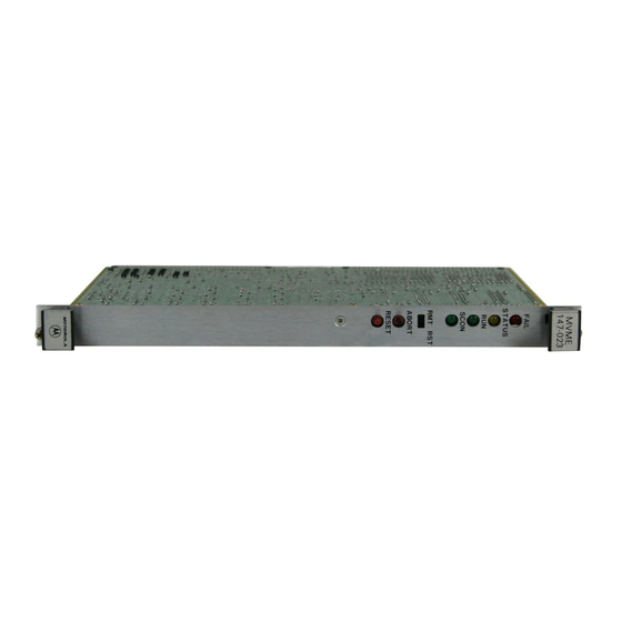
- Page 39 This chapter provides information on using the MVME147 in a system configuration. The following topics are presented: Controls and Indicators, page Memory Maps, page Controls and Indicators There are two switches on the front panel of the MVME147: ABORT RESET FAIL There are four LED status indicators on the...
- Page 40 FAIL when watchdog time-out occurs in the PCC. Also, if the LED is FAIL lit and SYSFAIL inhibit bit in the VMEchip is not set, the MVME147 drives SYSFAIL on the VMEbus. STATUS Indicator (DS2) The yellow LED, DS2, lights whenever the MC68030 STATUS STATUS* pin is low.
-
Page 41: Front Panel Indicators And Mvme147 Status
LED, DS3, is connected to the MC68030 address strobe (AS*) signal and indicates that the MPU is executing a bus cycle. SCON Indicator (DS4) The green LED, DS4, lights when the MVME147 is the SCON VMEbus system controller. Table 3-1. Front Panel Indicators and MVME147 Status FAIL... -
Page 42: Mvme147 Address Spaces
(VMEbus memory map). MC68030 Memory Map The MC68030 memory map is split into different address spaces by the function codes. The MVME147 has different groups of devices that respond depending on the address space as shown in Table 3-2. - Page 43 1. Onboard ROM/PROM/EPROM/EEPROM bank 1 for the Þrst 4 cycles after a reset, onboard DRAM thereafter. 2. DRAM size varies from 4MB to 32MB depending on the MVME147 model. 3. Size is approximate. 4. This A24 only applies to VMEbus space that falls below $01000000. VMEbus space below $01000000 only occurs on MVME147 models that have DRAMsize smaller than 16MB.
-
Page 44: Local I/O Devices
3. For a complete description of the register bits, refer to the data sheet for the speciÞc chip. 4. The LAN chip is not installed on the MVME147-010. Access to these addresses results in a local bus time-out. 5. The WD33C93 is interfaced in non-multiplexed mode. Only addresses $FFFE4000 (address/status register) and $FFFE4001 (data register) are necessary for operation. -
Page 45: Mc68882 Register Map
MOVES instructions), but the MVME147 has no devices that respond to them. Coprocessor Register Map The MC68882 is the only coprocessor on the MVME147. The map decoder selects the MC68882 any time the MPU executes a coprocessor cycle with Cp-ID of %001 (FC2-FC0 =%111 and A19- A13 =%0010001). - Page 46 MVME147 respond to such accesses. VMEbus Accesses to MVME147 Onboard DRAM When a VMEbus master accesses the MVME147 onboard DRAM, it must do so using the address modifier selected by a control register in the VMEchip and the base address selected by a control register in the PCC.
-
Page 47: Dram Address As Viewed From The Vmebus
Memory Maps Table 3-6. DRAM Address as Viewed from the VMEbus Beginning Ending RBA4 RBA3 RBA2 RBA1 RBA0 Address Address Notes $00000000 (1 x DRAMsize)-1 1 x DRAMsize (2 x DRAMsize)-1 1, 2 2 x DRAMsize (3 x DRAMsize)-1 1, 2 3 x DRAMsize (4 x DRAMsize)-1 1, 2 4 x DRAMsize (5 x DRAMsize)-1... - Page 48 Local Control and Status Register (LCSR) as shown in Table 3-7. A MVME147 may access its own VMEchip GCSR via the VMEbus. The MVME147 (and the MVME147Bug default) powers up with the GCSR base address programmed with $F. This is intentionally done so that the GCSR set is not mapped on the VMEbus.
-
Page 49: Vmechip Gcsr As Viewed From The Vmebus
IACKIN*, it responds by asserting IACKOUT* if it was not generating an interrupt at the acknowledged level, or by returning a status/ID vector if it was. The MVME147 may handle a VMEbus interrupt generated by its own VMEchip. 3-11... - Page 50 Operating Instructions 3-12...
- Page 51 4Programming Introduction This chapter provides the information needed to program the Peripheral Channel Controller (PCC) and the VMEchip. Programming the Peripheral Channel Controller These sections contain a description of the PCC internal registers and the bit assignments within each register. All registers may be written or read as bytes.
- Page 52 Programming Table 4-1. PCC Overall View 32-BIT REGISTERS Address Register Function FFFE1000 Table address (bits 1 and 0 are zeros) FFFE1004 Data address FFFE1008 Link -- 0000 -- DFC2-0 -- Byte count (24 bits) FFFE100C Data holding register 16-BIT REGISTERS Address Register Function...
- Page 53 Programming the Peripheral Channel Controller 8-BIT REGISTERS (Continued) Register Address Name Bit 7 Bit 6 Bit 5 Bit 4 Bit 3 Bit 2 Bit 1 Bit 0 FFFE1027 RsDis2 RsDis1 RsDis0 MIntEn LbToEn WWPar ParEn1 ParEn0 Gen. Purpose Cntrl (Note) (Note) (Note) FFFE1028...
- Page 54 Programming Table Address Register This 32-bit read/write register points to a table of physical addresses and byte counts that are used during DMA transfers when table mode is selected. The table address must be longword aligned because bits 0 and 1 are always zero. If the table address has bit 0 or 1 set, they are truncated and no error is generated.
- Page 55 Programming the Peripheral Channel Controller Byte Count Register This 32-bit read/write register contains a 24-bit byte counter in bits 0-23, a 3-bit function code in bits 24-26, and a link bit in bit 31. The byte counter contains the number of bytes to be transferred. The function code bits are used when data is transferred.
- Page 56 Programming Timer 1 Preload Register This 16-bit read/write register holds the tick timer preload value. When the counter reaches $FFFF, it is loaded with this value and if interrupts are enabled, an interrupt is generated. When running, the counter is incremented every 6.25 microseconds. The following equation should be used to determine the counter value (n) for a periodic interrupt of time t where t is in seconds.
- Page 57 Programming the Peripheral Channel Controller Timer 1 Interrupt Control Register ADDRESS BIT 7 BIT 6 BIT 5 BIT 4 BIT 3 BIT 2 BIT 1 BIT 0 FFFE1018 IntStat Enable Bit set and clear instructions should not be used on this Note interrupt control register.
- Page 58 Programming Timer 1 Control Register ADDRESS BIT 7 BIT 6 BIT 5 BIT 4 BIT 3 BIT 2 BIT 1 BIT 0 FFFE1019 Ovf3 Ovf2 Ovf1 Ovf0 ClrOvf EnaCnt Enable Bit 0 When this bit is low, the timer is disabled and the counter is loaded with the preload value.
- Page 59 Programming the Peripheral Channel Controller Timer 2 Interrupt Control Register ADDRESS BIT 7 BIT 6 BIT 5 BIT 4 BIT 3 BIT 2 BIT 1 BIT 0 FFFE101A IntStat Enable Bit set and clear instructions should not be used on this Note interrupt control register.
- Page 60 Programming Timer 2 Control Register ADDRESS BIT 7 BIT 6 BIT 5 BIT 4 BIT 3 BIT 2 BIT 1 BIT 0 FFFE101B Ovf3 Ovf2 Ovf1 Ovf0 ClrOvf EnaCnt Enable Bit 0 When this bit is low, the timer is disabled and the counter is loaded with the preload value.
- Page 61 Programming the Peripheral Channel Controller AC Fail Interrupt Control Register ADDRESS BIT 7 BIT 6 BIT 5 BIT 4 BIT 3 BIT 2 BIT 1 BIT 0 FFFE101C IntStat ACFail Enable Bit 3 When this bit is high, the interrupt is enabled. The interrupt is disabled when this bit is low.
- Page 62 This bit is cleared by reset. This bit should only be set if the MVME147 is system controller. Bit 3 This bit is set if the watchdog timer times out. This bit is cleared by writing a 1 to it.
- Page 63 Programming the Peripheral Channel Controller Printer Interrupt Control Register ADDRESS BIT 7 BIT 6 BIT 5 BIT 4 BIT 3 BIT 2 BIT 1 BIT 0 FFFE101E IntStat FaltInt ACKInt ACKPol Enable Bit set and clear instructions should not be used on this Note control register.
- Page 64 Programming Printer Control Register ADDRESS BIT 7 BIT 6 BIT 5 BIT 4 BIT 3 BIT 2 BIT 1 BIT 0 FFFE101F InPrim Strobe StbTim Mode Bit 0 This bit selects the auto or manual mode for the printer strobe. When this bit is low, the printer strobe is generated by a write to the printer data register (auto mode).
- Page 65 Programming the Peripheral Channel Controller DMA Interrupt Control Register ADDRESS BIT 7 BIT 6 BIT 5 BIT 4 BIT 3 BIT 2 BIT 1 BIT 0 FFFE1020 IntStat Enable Bit set and clear instructions should not be used on this Note control register.
- Page 66 Programming DMA Control and Status Register ADDRESS BIT 7 BIT 6 BIT 5 BIT 4 BIT 3 BIT 2 BIT 1 BIT 0 FFFE1021 DONE 8BitEr TblSizEr DMABEr TWBEr MS/SM* Enable All bits are cleared by reset. Note Bit 0 When this bit is low, the DMA controller is disabled and status bits 3-7 are reset.
- Page 67 Programming the Peripheral Channel Controller Bus Error Interrupt Control Register ADDRESS BIT 7 BIT 6 BIT 5 BIT 4 BIT 3 BIT 2 BIT 1 BIT 0 FFFE1022 IntStat Enable Bit 3 When this bit is high, the interrupt is enabled. The interrupt is disabled when this bit is low.
- Page 68 Programming DMA Status Register ADDRESS BIT 7 BIT 6 BIT 5 BIT 4 BIT 3 BIT 2 BIT 1 BIT 0 FFFE1023 Inc 4 Inc 3 Inc 2 Inc 1 Bits 0-3 The PCC has a 32-bit register which is used to hold data that is transferred between the SCSI bus and the local bus.
- Page 69 Programming the Peripheral Channel Controller Abort Interrupt Control Register ADDRESS BIT 7 BIT 6 BIT 5 BIT 4 BIT 3 BIT 2 BIT 1 BIT 0 FFFE1024 IntStat Abort Enable Bit set and clear instructions should not be used on this Note control register.
- Page 70 This function code is placed on the local bus when the DMA address table is accessed. Note that a value of 1, 2, 5, or 6 must be placed in Tbl FC2-FC0 for proper operation of the MVME147 during table walking. These bits are cleared by reset.
- Page 71 Programming the Peripheral Channel Controller Serial Port Interrupt Control Register ADDRESS BIT 7 BIT 6 BIT 5 BIT 4 BIT 3 BIT 2 BIT 1 BIT 0 FFFE1026 IntStat Int/Ext* Enable All bits are cleared by reset. Note Bits 0-2 These bits program the interrupt level that the serial ports generate.
- Page 72 BIT 2 BIT 1 BIT 0 FFFE1027 RsDis2 RsDis1 RsDis0 MIntEn LbToEn WWPar ParEn1 ParEn0 Bits 0-1 These bits control local RAM parity checking. These bits should not be enabled on the MVME147-010. These bits are cleared by reset. 4-22...
- Page 73 Programming the Peripheral Channel Controller The DRAM parity on the MVME147 is in an undefined Note state after power-up. Reads to uninitialized memory with parity checking enabled causes bus errors. All DRAM locations should be written to ensure correct parity before checking is enabled.
- Page 74 Programming LAN Interrupt Control Register Note The LAN interrupt is not used on the MVME147-010 and should not be enabled. ADDRESS BIT 7 BIT 6 BIT 5 BIT 4 BIT 3 BIT 2 BIT 1 BIT 0 FFFE1028 IntStat Enable Note All bits are cleared by reset.
- Page 75 Programming the Peripheral Channel Controller General Purpose Status Register ADDRESS BIT 7 BIT 6 BIT 5 BIT 4 BIT 3 BIT 2 BIT 1 BIT 0 FFFE1029 PuReset ParErr Bit 0 This bit is set when a parity error occurs while the local processor is accessing RAM.
- Page 76 Bit 4 This bit is used to control the reset signal on the SCSI bus. When this bit is low, the SCSI reset signal is not driven by MVME147. When this bit is high, the SCSI reset is driven by MVME147.
- Page 77 Programming the Peripheral Channel Controller Slave Base Address Register ADDRESS BIT 7 BIT 6 BIT 5 BIT 4 BIT 3 BIT 2 BIT 1 BIT 0 FFFE102B LANA25 LANA24 WAITRMC RBA4 RBA3 RBA2 RBA1 RBA0 Note All bits are cleared by reset. Bits 0-4 These bits set the slave RAM base address, or the address of onboard RAM as viewed from the VMEbus.
- Page 78 Programming Table 4-2. DRAM Address as Viewed from the VMEbus (Continued) Beginning Ending RBA4 RBA3 RBA2 RBA1 RBA0 Notes Address Address 16 x DRAMsize (17 x DRAMsize)-1 1, 2 17 x DRAMsize (18 x DRAMsize)-1 1, 2 18 x DRAMsize (19 x DRAMsize)-1 1, 2 19 x DRAMsize (20 x DRAMsize)-1 1, 2...
- Page 79 MARMC cycles (only guaranteed if the other master implements MARMC cycles the same way as the MVME147). When WAITRMC is cleared, the MVME147 only waits for VMEbus mastership if the MARMC cycle starts out by going to the VMEbus. Note...
- Page 80 Programming Software Interrupt 1 Control Register ADDRESS BIT 7 BIT 6 BIT 5 BIT 4 BIT 3 BIT 2 BIT 1 BIT 0 FFFE102C IntStat Enable All bits are cleared by reset. Note Bits 0-2 These bits program the interrupt level that is generated. Level 0 does not generate an interrupt.
- Page 81 Programming the Peripheral Channel Controller Interrupt Vector Base Register ADDRESS BIT 7 BIT 6 BIT 5 BIT 4 BIT 3 BIT 2 BIT 1 BIT 0 FFFE102D IVB7 IVB6 IVB5 IVB4 Bits 4-7 These bits are used to form the base interrupt status/ID vector for interrupts whose vectors originate from the PCC.
- Page 82 Programming Software Interrupt 2 Control Register ADDRESS BIT 7 BIT 6 BIT 5 BIT 4 BIT 3 BIT 2 BIT 1 BIT 0 FFFE102E IntStat Enable All bits are cleared by reset. Note Bits 0-2 These bits program the interrupt level that is generated. Level 0 does not generate an interrupt.
- Page 83 Programming the Peripheral Channel Controller Revision Level Register ADDRESS BIT 7 BIT 6 BIT 5 BIT 4 BIT 3 BIT 2 BIT 1 BIT 0 FFFE102F RevL7 RevL6 RevL5 RevL4 RevL3 RevL2 RevL1 RevL0 Bits 0-7 These bits represent the revision level of the PCC. Initial parts are released as level 0.
- Page 84 Programming Printer Data Register ADDRESS BIT 7 BIT 6 BIT 5 BIT 4 BIT 3 BIT 2 BIT 1 BIT 0 FFFE2800 Bits 0-7 These bits form the printer data lines. They are write only. Reading this address accesses the printer status register. These bits are not affected by reset.
- Page 85 Programming the Peripheral Channel Controller Printer Status Register ADDRESS BIT 7 BIT 6 BIT 5 BIT 4 BIT 3 BIT 2 BIT 1 BIT 0 FFFE2800 FAULT SELECT STAT12 All of these bits are read only. Writing this address Note accesses the printer data register.
- Page 86 Programming Programming the VMEchip The VMEchip has two groups of registers: the Local Control and Status Registers (LCSR) and the Global Control and Status Registers (GCSR). Programming the LCSR There are 14 LCSR registers as shown in Table 4-4. Table 4-4. VMEchip Local Control and Status Registers Register Address Name...
- Page 87 J3. When J3 pins 1 and 2 are connected, enabling the MVME147 to act as the VMEbus system controller, then SCON = 1. When J3 pins 1 and 2 are not connected, the MVME147 is not the VMEbus system controller and SCON = 0.
- Page 88 These bits are set to 1, 1 by any reset. Note that writes to REQLEV1,0 do not change the actual requester level until the MVME147 goes through the action of having VMEbus mastership and releasing it. This means that there are times when the value written into REQLEV1,0 do not match the current requester level (the request level is lagging).
- Page 89 200 ns. This bit is cleared by any reset. Bit 6 The DHB status bit is 1 when the MVME147 is VMEbus master and 0 when it is not. Bit 7 Setting the DWB control bit to 1 causes the VMEchip to request the VMEbus (if not already bus master).
- Page 90 FFFE2005 DDTACK 020 MASWP CFILL MASUAT MASA16 MASA24 MASD16 Bit 0 Setting the MASD16 bit forces the MVME147 to perform only D8 and D16 data transfers on the VMEbus. Clearing the MASD16 bit allows D8, D16, and D32 transfer capability on the VMEbus when the MC68030 accesses in the range below $F0000000.
- Page 91 Programming the VMEchip Table 4-5. Determining the Master AM Code VMEbus Address ModiÞer Code T = True, F = False, X = Don't Care Notes AM2, 1, 0 track FC2, 1, 0. ADR16 = T represents MC68030 accesses to the VMEbus above $FFFF0000. ADR16 = F represents MC68030 accesses to the VMEbus below $FFFF0000.
- Page 92 Programming Bit 3 The MASUAT bit allows software to conÞgure the master to provide the UAT data transfer capability. Setting the MASUAT bit to 1 conÞgures the master to execute unaligned VMEbus cycles when necessary. If the bit is cleared, the MC68030 is acknowledged so as to break the unaligned transfer into multiple aligned cycles.
- Page 93 VMEchip to complete the write to onboard DRAM on its own. This bit is cleared by SYSRESET. Bit 7 Setting SLVEN to 1 enables other VMEbus masters to access the MVME147 onboard DRAM. This bit is cleared by SYSRESET. 4-43...
- Page 94 Programming Timer Configuration Register ADDRESS BIT 7 BIT 6 BIT 5 BIT 4 BIT 3 BIT 2 BIT 1 BIT 0 FFFE2009 ARBT0 VBTO1 VBTO0 ACTO1 ACTO0 LBTO1 LBTO0 Bits 0-1 These two bits conÞgure the local time-out period. They are set to 1 by any reset.
- Page 95 Setting ARBTO to 1 enables the VMEbus arbitration timer. The VMEbus arbitration timer activates BBSY* if it is not activated within 410 µs after the MVME147 arbiter issues a bus grant. The timer deactivates BBSY* as speciÞed in the VMEbus speciÞcation.
- Page 96 Programming Slave Address Modifier Register ADDRESS BIT 7 BIT 6 BIT 5 BIT 4 BIT 3 BIT 2 BIT 1 BIT 0 FFFE200B SUPER USER EXTED STND SHORT BLOCK PRGRM DATA This register allows software to configure which Note address modifier codes the VMEbus masters must use to access the onboard DRAM.
- Page 97 Programming the VMEchip Although all bits in the slave address modifier register Note may be changed dynamically, they must be changed only when the VMEchip has control of the VMEbus. The recommended procedure for changing the slave address modifier is: a.
- Page 98 FFFE200D AMSEL The register allows software to program the address Note modifier code that is driven by the MVME147 during a VMEbus cycle. Bits 0-5 These Þve bits, in conjunction with AMSEL, allow software to select dynamically the address space that the master accesses during VMEbus cycles.
- Page 99 Programming the VMEchip Interrupt Handler Mask Register ADDRESS BIT 7 BIT 6 BIT 5 BIT 4 BIT 3 BIT 2 BIT 1 BIT 0 FFFE200F IEN7 IEN6 IEN5 IEN4 IEN3 IEN2 IEN1 This register is used to enable the MC68030 to respond Notes to specific VMEbus interrupt requests.
- Page 100 Programming Utility Interrupt Mask Register ADDRESS BIT 7 BIT 6 BIT 5 BIT 4 BIT 3 BIT 2 BIT 1 BIT 0 FFFE2011 WPERREN SFIEN SIGHEN LM1EN IACKEN LM0EN SIGLEN Note This register is used to enable the VMEchip interrupt handler to respond to specific utility interrupt requests.
-
Page 101: Utility Interrupts And Their Assigned Level
Programming the VMEchip Bit 4 As described in the Programming the GCSR section in this chapter, the GCSR provides four location monitors. Two of them, location monitor 0 and 1, cause a local interrupt when the VMEbus address they are conÞgured to monitor is accessed. The LM1EN control bit allows software to mask the interrupt requested when an access is detected to the address monitored by location monitor 1. - Page 102 Programming Utility Interrupt Vector Register ADDRESS BIT 7 BIT 6 BIT 5 BIT 4 BIT 3 BIT 2 BIT 1 BIT 0 FFFE2013 UVB7 UVB6 UVB5 UVB4 UVB3 UID2 UID1 UID0 Notes The utility interrupt vector register provides the local CPU with a unique vector for each of the utility interrupts.
- Page 103 Programming the VMEchip Table 4-7. Encoding of the Interrupt ID Utility Bit 2 Bit 1 Bit 0 Interrupt Source SIGLP IACK SIGHP SYSFAIL WPBERR 4-53...
- Page 104 Programming Interrupt Request Register ADDRESS BIT 7 BIT 6 BIT 5 BIT 4 BIT 3 BIT 2 BIT 1 BIT 0 FFFE2015 This register is used to configure the interrupt request Note line that the interrupter activates to request an interrupt on the VMEbus.
- Page 105 Programming the VMEchip When the bits are set to drive one of the IRQ lines, they Note must not be changed. The three bits may be changed only when they are all cleared, signifying that the previous interrupt request has been serviced. An added function provided by setting IACKEN (refer to the Utility Interrupt Mask Register section in this chapter) is provided by the VMEchip to signal the local...
- Page 106 Programming VMEbus Status/ID Register ADDRESS BIT 7 BIT 6 BIT 5 BIT 4 BIT 3 BIT 2 BIT 1 BIT 0 FFFE2017 This register allows software to program dynamically Note the status/ID that the interrupter provides during an interrupt acknowledge cycle. D00-D03 are set by SYSRESET, D04-D07 are cleared by SYSRESET.
- Page 107 Programming the VMEchip Bus Error Status Register ADDRESS BIT 7 BIT 6 BIT 5 BIT 4 BIT 3 BIT 2 BIT 1 BIT 0 FFFE2019 RMCERR VBERR ACTO LBTO This register allows the MC68030 to determine the Note cause of a bus error condition flagged by the VMEchip. Reading the register causes all of its bits to be cleared to 0.
-
Page 108: Vmechip Gcsr As Viewed From The Vmebus
Programming GCSR Base Address Configuration Register ADDRESS BIT 7 BIT 6 BIT 5 BIT 4 BIT 3 BIT 2 BIT 1 BIT 0 FFFE201B GCSRA7 GCSRA6 GCSRA5 GCSRA4 Note This register allows software to set the base address of the GCSR set of registers in the VMEbus supervisor short I/O map. - Page 109 Programming the VMEchip Programming the GCSR There are eight GCSR registers as shown in Table 4-10. The VMEbus address is in the supervisor short I/O map. Table 4-10. VMEchip Global Control and Status Register MVME147 VMEbus Register Name Address Address...
- Page 110 Programming Global Register 0 MVME147 VMEbus ADDRESS ADDRESS BIT 7 BIT 6 BIT 5 BIT 4 BIT 3 BIT 2 BIT 1 BIT 0 FFFE2021 00X1 LM0 CHIPID3 CHIPID2 CHIPID1 CHIPID0 MC68030 VMEbus Bits 0-3 These bits provide a unique identiÞcation number for the VMEchip.
- Page 111 Programming the VMEchip Bit 7 Location monitor 3 is conÞgured to monitor double-byte accesses to the supervisor short I/O address $00F6, and single- byte accesses to the short I/O address $00F7. When cleared, LM3 indicates that an access to address $00F6 or $00F7 was detected.
- Page 112 Programming Global Register 1 MVME147 VMEbus ADDRESS ADDRESS BIT 7 BIT 6 BIT 5 BIT 4 BIT 3 BIT 2 BIT 1 BIT 0 FFFE2023 00X3 R&H SCON BRDFAIL SIGHP SIGLP MC68030 VMEbus Bit 0 The SIGLP control signal allows other VMEbus masters to interrupt the MC68030.
- Page 113 0. Bit 7 The R&H bit allows other VMEbus masters to reset the MVME147. The MVME147 is held in the reset state for as long as the R&H bit is set. This bit is cleared by SYSRESET. Notes 1. The GCSR Base Address Configuration Register...
- Page 114 Programming Board Identification Register MVME147 VMEbus ADDRESS ADDRESS BIT 7 BIT 6 BIT 5 BIT 4 BIT 3 BIT 2 BIT 1 BIT 0 FFFE2025 00X5 BRDID7 BRDID6 BRDID5 BRDID4 BRDID3 BRDID2 BRDID1 BRDID0 MC68030 VMEbus Note The MC68030 can both read and write to this register.
- Page 115 Programming the VMEchip General Purpose CSR 0 MVME147 VMEbus ADDRESS ADDRESS BIT 7 BIT 6 BIT 5 BIT 4 BIT 3 BIT 2 BIT 1 BIT 0 FFFE2027 00X7 General Purpose Control and Status Register 0 MC68030 VMEbus Note General purpose CSR 0 is both readable and writable from the MC68030 and from the VMEbus.
- Page 116 Programming General Purpose CSR 1-4 MVME147 VMEbus ADDRESS ADDRESS BIT 7 BIT 6 BIT 5 BIT 4 BIT 3 BIT 2 BIT 1 BIT 0 FFFE2029 00X9 General Purpose Control and Status Register 1 FFFE202B 00XB General Purpose Control and Status Register 2...
- Page 117 Two tick timers Watchdog timer Four ROM sockets SCSI bus interface with DMA Ethernet transceiver interface Centronics printer port A32/D32 VMEbus interface VMEbus system controller Numerous control functions Note that the Ethernet interface is not included on the MVME147- 010.
- Page 118 Functional Description MC68030 MPU The MC68030 is the main processor of the MVME147. The MC68030 has onchip instruction and data caches. The MVME147 prevents the MC68030 from caching accesses to any other device than local DRAM by activating the cache inhibit in pin (CIIN*) during the accesses.
- Page 119 VMEchip Figure 5-1. MVME147 Block Diagram...
- Page 120 The system reset utility is also described here because it is enabled when the MVME147 is system controller. The system controller function is enabled/disabled by header J3. When the MVME147 is system controller, the System Controller (SCON) LED is turned on.
- Page 121 MVME147 enables/disables its SYSRESET* function at the same time that it enables/disables its system controller functions. When the MVME147 is system controller, it drives the SYSRESET* signal line whenever an onboard reset is generated (it does not fully implement the SYSRESET* timing of a VMEbus power monitor).
- Page 122 VMEbus Access Time-Out The VMEchip provides a VMEbus access time-out timer. If the MVME147 is not granted the VMEbus within the selected time period, the MC68030 receives a bus error signal (unless the cycle is write posted). The time period is selectable in software for 102 µs, 1.6 ms, 51 ms, or infinite.
- Page 123 VMEchip VMEbus Requester The VMEbus requester is used to obtain and relinquish mastership of the VMEbus. Its operation is affected by software programmable bits in the VMEchip. The requester requests VMEbus mastership at the programmed level when the board is not the current VMEbus master and one of the following happens: The MC68030 executes a program space cycle that is bound for the VMEbus.
- Page 124 DRAM while the WAITRMC bit was set in the PCC. VMEbus Slave Interface The VMEchip provides the VMEbus slave interface for the MVME147. When the VMEbus wants to access the DRAM or VMEchip control registers, the VMEbus map decoder selects the VMEchip.
- Page 125 MVME147 single board computers. It provides the interface between the MC68030, VMEchip, PCC, LANCE, and DRAM on the MVME147. While preserving the original function of the MVME147, the GCC lowers part and manufacture cost and reduces power consumption. The GCC includes the following features: Local DRAM controller: Ð...
- Page 126 Functional Description RAM Refresh Timer The DRAM used on the MVME147 must be refreshed at least every 15.6 µs. The GCC provides a refresh signal to the DRAM at least once every 15.6 µs. Local Bus Multiport Arbiter Because the local address and data buses are used to access the onboard DRAM and the VMEbus, any devices that use these resources must become the local bus master first.
- Page 127 Peripheral Channel Controller (PCC) Peripheral Channel Controller (PCC) The PCC is an ASIC device designed for the MVME147. The PCC includes the following features: DMA channel for SCSI data 8-bit to 32-bit converter for SCSI data SCSI chip interface Local processor interrupter/handler...
- Page 128 Functional Description DMAC Initiation Mode The DMAC has two initiation modes: direct and command chaining (scatter-gather). In the direct mode, the data address pointer and the byte count are loaded into the chip. In the command chaining mode, a table of data addresses and byte counts is placed in local RAM and the address of the table is loaded into the chip.
- Page 129 Peripheral Channel Controller (PCC) using the address contained in the data address register. Data transfers continue until the byte count register reaches 0. At this point, the DMAC sets the done bit and enters the idle state unless more table walking is indicated by the link bit in the byte count register.
- Page 130 Functional Description SCSI Data Bus Converter The WD33C93 connects to a separate 8-bit data bus on the PCC and not to the local MC68030 bus. This allows the PCC to collect one longword of data by transferring one byte at a time from the WD33C93 without using the processor bus.
- Page 131 Control and Status Registers The PCC has input and output signal lines for controlling various functions on the MVME147. There are control lines for DRAM parity enable, parity test and parity error status, VMEbus map select, multiple address RMC mode, and LANCE address select.
- Page 132 All four serial ports use EIA-232-D drivers and receivers located on the MVME147 and all the signal lines are routed to P2. The configuration headers are located on the MVME147 and the MVME712. An external I/O transition board such as the MVME712 must be used to convert the P2 pin out to industry standard connectors.
- Page 133 Every MVME147 is assigned an Ethernet station address. The address is $08003E2xxxxx where xxxxx is the unique number assigned to the module (i.e., every MVME147 has a different value for xxxxx). Each Ethernet station address is displayed on a label attached to the MVME147Õs backplane connector P2.
- Page 134 Ethernet station address. SCSI Interface The MVME147 has a SCSI mass storage bus interface. The SCSI bus is provided to allow mass storage subsystems to be connected to the MVME147. These subsystems may include hard and floppy disk drives, streaming tape drives, and other mass storage devices.
- Page 135 ROM/PROM/EPROM/EEPROM There are four 32-pin ROM/PROM/EPROM/EEPROM sockets on the MVME147. They are organized as 2 banks with two sockets per bank. The banks are configured as word ports to the MPU. Each bank can be separately configured for 8K x 8, 16K x 8, 32K x 8, 64K x 8, 128K x 8, 256K x 8, 512K x 8, or 1M x 8 ROM/PROM/EPROM devices or 2K x 8, 8K x 8, or 32K x 8 EEPROM devices.
- Page 136 Address valid to data valid CE* low to data valid OE* low to data valid Address invalid, CE* or OE* high to data not valid CE* or OE* high to data high impedance Figure 5-2. Timings Required by the MVME147 5-20...
- Page 137 OE* high to WE* low Address invalid after WE* low WE* low pulse width Data valid to WE* high WE* high to data not valid WE* high to OE* low WE* high to CE* high Figure 5-3. Timings Guaranteed by MVME147 5-21...
- Page 138 Functional Description EEPROM Power-Up/Power-Down Considerations The MVME147 provides no protection against inadvertent writes to EEPROM that might happen at power-up or power-down time. Most devices provide some level of internal protection. To gain Òabsolute protectionÓ devices with additional Òsoftware protectionÓ are recommended.
- Page 139 Interrupt Handler Table 5-2. MVME147 Interrupt Sources and Vectors Interrupt Path Vector Source Vector Level Source ACFAIL %xxxx0000 BERR %xxxx0001 ABORT %xxxx0010 Z8530 devices See Z8530 data sheet Prog Serial Ports %xxxx0011 Prog LANCE %xxxx0100 Prog SCSI Port %xxxx0101 Prog...
- Page 140 (address $FFFE102D) bits 4 through 7. yyyyy is the value programmed into the VMEchip utility interrupt vector register (address $FFFE2013) bits 3 through 7. Front Panel Switches and Indicators There are two switches on the front panel of the MVME147. The switches are RESET ABORT...
- Page 141 VMEbus. It is specifically optimized for the MC68030. The parity feature is not implemented on the MVME147-010. The MVME147 has parity check which operates in one of three user selectable modes. In mode 1, no parity checking is performed and the DRAM operates at maximum speed.
- Page 142 Functional Description VMEbus DRAM Accesses When the VMEbus map decoder detects an onboard DRAM select, the VMEchip requests local bus mastership from the GCC multiport arbiter. When the GCC multiport arbiter has granted local bus mastership, a DRAM read or write cycle happens and the VMEchip activates the DTACK* (or BERR* if parity is enabled and a parity error occurs) signal on the VMEbus.
- Page 143 RAM sequencer perform a Column Address Strobe (CAS) before Row Address Strobe (RAS) refresh cycle. Reset There are five sources of reset on the MVME147: SYSRESET* -- Resets all onboard devices. Power on reset -- Resets all onboard devices and drives SYSRESET* if this board is system controller.
- Page 144 Functional Description Sources of Bus Error (BERR*) The devices on the MVME147 that are capable of activating a local bus error are described below. Local Bus Time-Out A Local Bus Time-Out (LBTO) occurs whenever an MPU or PCC access (outside of the VMEbus range) does not complete within the programmed time.
- Page 145 Because different conditions can cause bus error exceptions, the software must be able to distinguish the source. To aid in this, the MVME147 provides status bits in the VMEchip and PCC chip. Generally, the bus error handler can interrogate the status bits and proceed with the result.
- Page 146 MVME147 Support of MC68030 Indivisible Cycles The MC68030 performs operations that require indivisible cycle sequences to the local DRAM and to the VMEbus. The MVME147 requires special circuitry to support these operations. Indivisible accesses to a single address are called Single Address Read-Modify- Write Cycles (SARMC).
- Page 147 AEIA-232-D Interconnections Introduction The EIA-232-D standard is the most common terminal/computer and terminal/modem interface, and yet it is not fully understood. This may be because not all the lines are clearly defined, and many users do not see the need to follow the standard in their applications.
- Page 148 EIA-232-D Interconnections Table A-1. EIA-232-D Interconnections Signal Number Mnemonic Signal Name and Description CHASSIS GROUND. Not always used. See section Proper Grounding. TRANSMIT DATA. Data to be transmitted; input to the modem from the terminal. RECEIVE DATA. Data which is demodulated from the receive line;...
- Page 149 Levels of Implementation Table A-1. EIA-232-D Interconnections (Continued) Signal Number Mnemonic Signal Name and Description RING INDICATOR. Output from the modem to the terminal; indicates to the terminal that an incoming call is present. The terminal causes the modem to answer the phone by carrying DTR true while RI is active.
- Page 150 EIA-232-D Interconnections usually necessary to make CTS high by connecting it to RTS or to some source of +12 volts such as the resistors shown in Figure A-1. CTS is also frequently jumpered to an MC1488 gate which has its inputs grounded (the gate is provided for this purpose).
- Page 151 Levels of Implementation SERIAL PORT 1488 1489A 39kΩ -12V CONNECTOR +12V LS08 TERMINAL 470Ω 470Ω 470Ω OPTIONAL HARDWARE TRANSPARENT SIG GND MODE CHASSIS GND LOGIC LS08 +12V SIG GND 470Ω 1488 SERIAL PORT 1489A CONNECTOR 39kΩ -12V MODEM 1488 HOST 470Ω...
- Page 152 EIA-232-D Interconnections Figure A-2 shows a way of wiring an EIA-232-D connector to enable a computer to connect to a basic terminal with only three lines. This is feasible because most terminals have DTR and RTS signals that are ON, and which can be used to pull up the CTS, DCD, and DSR signals.
- Page 153 Levels of Implementation Proper Grounding Another subject to consider is the use of ground pins. There are two pins labeled GND. Pin 7 is the SIGNAL GROUND and must be connected to the distant device to complete the circuit. Pin 1 is the CHASSIS GROUND, but it must be used with care.
- Page 154 EIA-232-D Interconnections...
- Page 155 User friendliness Portability Ease of maintenance This member of the M68000 firmware family is implemented on the MVME147 MPU VMEmodule and is known as MVME147Bug, or simply 147Bug. Description of 147Bug The MVME147Bug package is a powerful evaluation and debugging tool for systems built around the MVME147 monoboard microcomputer.
- Page 156 A command-driven user-interactive software debugger, described in this appendix, and hereafter referred to as Òthe debuggerÓ or Ò147BugÓ A command-driven diagnostic package for the MVME147 hardware, hereafter referred to as Òthe diagnosticsÓ A user interface which accepts commands from the system...
- Page 157 Debugging Package UserÕs Manual) and an expanded online help facility. If you have used one or more of Motorola's other debugging packages, you will find the 147Bug very similar. Considerable effort has also been made to make the interactive commands more consistent.
- Page 158 Eight bits per character One stop bit per character Parity disabled (no parity) Baud rate 9600 baud (default baud rate of all MVME147 ports at power-up) After power-up, the baud rate of the debug port can be reconfigured by using the Port Format (PF) command of the 147Bug debugger.
- Page 159 1. Power must have just been applied (but the RB command can change this to also respond to any reset). 2. Your routine must be located within the MVME147 ROM memory map (but the RB command can change this to any other portion of the onboard memory, or even offboard VMEbus memory).
- Page 160 Routine Name ASCII string containing routine name. By convention within Motorola, the checksum is placed in the two bytes following the routine. If you wish to make use of ROMboot you do not have to fill a complete ROM. Any partial amount is acceptable, as long as the length reflects where the checksum is correct.
- Page 161 ROMboot 4. Search local RAM (if RB command has selected to operate on any reset), at all 8K byte boundaries starting at $00006000. 5. Search the VMEbus map (if so selected by the RB command) on all 8K byte boundaries starting at the end of the onboard RAM.
- Page 162 Debugger General Information md 6018;di Disassemble executable instructions 147-Bug> 00006018 4E4F0026 SYSCALL .PCRLF 0000601C 4E4F0052 SYSCALL .RTC_DSP 00006020 4E4F0026 SYSCALL .PCRLF 00006024 4E4F0026 SYSCALL .PCRLF 00006028 4E4F0063 SYSCALL .RETURN 0000602C 00000000 ORI.B #$0,D0 00006030 00000000 ORI.B #$0,D0 00006034 00000000 ORI.B #$0,D0 CS 6000 602E Perform checksum on locations 6000...
- Page 163 During COLD reset mode, a total board initialization takes place, as if the MVME147 had just been powered up. The breakpoint table and offset registers are cleared. The user registers are invalidated. Input and output character queues are cleared. Onboard devices (timer, serial ports, etc.) are reset.
- Page 164 Abort is invoked by pressing and releasing the switch on the ABORT MVME147 front panel. Whenever Abort is invoked when executing a user program (running target code), a ÒsnapshotÓ of the processor state is captured and stored in the target registers. (When working in the debugger, Abort captures and stores only the program counter, status register, and format/vector information.) For this...
- Page 165 Restarting the System Environment is set for Bug mode. Automatic SCSI bus reset is turned off. Onboard diagnostic switch is turned on (for this reset only). System memory sizing is turned on (System mode). Console is set to port 1 (LUN 0). Port 1 (LUN 0) is set to use ROM defaults for initialization.
- Page 166 SCSI firmware code is not position-independent. 147Bug requires a minimum of 16KB of contiguous read/write memory to operate. This memory is the MVME147 on-board RAM and is used for 147Bug stack and static variable space. The rest of on-board RAM is reserved as user space.
- Page 167 Terminal Input/Output Control Terminal Input/Output Control When entering a command at the prompt, the following control codes may be entered for limited command line editing. Note The presence of the caret ( ^ ) before a character indicates that the Control ( ) key must be held CTRL down while striking the character key...
- Page 168 Debugger General Information Disk I/O Support 147Bug can initiate disk input/output by communicating with intelligent disk controller modules over the VMEbus. Disk support facilities built into 147Bug consist of: Command-level disk operations Disk I/O system calls (only via one of the TRAP #15 instructions) for use by user programs Defined data structures for disk parameters Parameters such as these:...
- Page 169 Disk I/O Support If the conversion from blocks to sectors yields a fractional sector count, an error is returned and no data is transferred. Disk I/O via 147Bug Commands The 147Bug commands listed in the following paragraphs are provided for disk I/O. Detailed instructions for their use are found in MVME147BUG 147Bug Debugging Package UserÕs Manual.
- Page 170 Debugger General Information BO (Bootstrap Operating System) BO reads an operating system or control program from the specified device into memory, then transfers control to it. BH (Bootstrap and Halt) BH reads an operating system or control program from a specified device into memory, then returns control to 147Bug.
- Page 171 Disk I/O Support To perform a disk operation, 147Bug must eventually present a particular disk controller module with a controller command packet which has been especially prepared for that type of controller module. (This is accomplished in the respective controller driver module.) A command packet for one type of controller module usually does not have the same format as a command packet for a different type of module.
- Page 172 147Bug returns an error code if an attempted disk operation is unsuccessful. Multiprocessor Support The MVME147 dual-port RAM feature makes the shared RAM available to remote processors as well as to the local processor. A remote processor can initiate program execution in the local MVME147 dual-port RAM by issuing a remote GO command using the Multiprocessor Control Register (MPCR).
- Page 173 Disk I/O Support The codes stored in the MPCR are of two types: Status returned (from 147Bug) Command set by the bus master (job requested by some processor) The status codes that may be returned from 147Bug are: HEX 0 (HEX 00) Wait.
- Page 174 Debugger General Information The MPCR contains $00 at power-up, indicating that initialization is not yet complete. As the initialization proceeds, the execution path comes to the ÒpromptÓ routine. Before sending the prompt, this routine places an R in the MPCR to indicate that initialization is complete.
-
Page 175: Diagnostic Utilities
Included in the 147Bug package is a complete set of hardware diagnostics intended for testing and troubleshooting of the MVME147. These diagnostics are listed in the following tables. In order to use the diagnostics, you must switch directories to the diagnostic directory. -
Page 176: Diagnostic Test Commands
Debugger General Information Table 5-3. Diagnostic Test Commands Command Description MPU tests for the MC68030 CA30 MC68030 onchip cache tests Memory tests Memory Management Unit tests Real-time clock tests Bus error test BERR Floating-point coprocessor (MC68882) test LANCE chip (AM7990) functionality test LANX LANCE chip (AM7990) external test Z8530 functionality test... - Page 177 Using the 147Bug Debugger Using the 147Bug Debugger Entering Debugger Command Lines 147Bug is command-driven and performs its various operations in response to user commands entered at the keyboard. When the debugger prompt ( ) appears on the terminal screen, then 147-Bug>...
- Page 178 Debugger General Information The commands are shown using a modified Backus-Naur form syntax. The metasymbols used are: boldface strings A boldface string is a literal such as a command or a program name, and is to be typed just as it appears. italic strings An italic string is a Òsyntactic variableÓ...
- Page 179 Using the 147Bug Debugger Expression as a Parameter An expression can be one or more numeric values separated by the arithmetic operators: Plus (+) Minus (-) Multiplied by (*) Divided by (/) Logical AND (&) Shift left (<<), or Shift right (>>). Numeric values may be expressed in either: Hexadecimal Decimal...
- Page 180 Debugger General Information A numeric value may also be expressed as a string literal of up to four characters. The string literal must begin and end with the single quote mark ('). The numeric value is interpreted as the concatenation of the ASCII values of the characters. This value is right-justified, as any other numeric value would be.
- Page 181 Using the 147Bug Debugger Address as a Parameter Many commands use addr as a parameter. The syntax accepted by 147Bug is similar to the one accepted by the MC68030 one-line assembler. All control addressing modes are allowed. An Òaddress + offset registerÓ mode is also provided. Address Formats Table B-4 summarizes the address formats which are acceptable for...
- Page 182 Debugger General Information Table B-4. Debugger Address Parameter Formats (continued) Notes 1. N Absolute address (any valid expression) Address register n Index register n (An or Dn) Displacement (any valid expression) Base displacement (any valid expression) Outer displacement (any valid expression) Register number (0 to 7) Offset register n 2.
- Page 183 Using the 147Bug Debugger Example: A portion of the listing file of an assembled, relocatable module is shown below: * MOVE STRING SUBROUTINE 0 00000000 48E78080 MOVESTR MOVEM.L D0/A0,—(A7) 0 00000004 4280 CLR.L 0 00000006 1018 MOVE.B (A0)+,D0 0 00000008 5340 SUBQ.W #1,D0 0 0000000A 12D8...
- Page 184 The valid port numbers which may be used for these commands are: 0 - MVME147 EIA-232-D (MVME712/MVME712M serial port 1) 1 - MVME147 EIA-232-D (MVME712/MVME712M serial port 2) 2 - MVME147 EIA-232-D (MVME712/MVME712M serial port 3)
- Page 185 147Bug MM command as outlined above and stored to the host using the Dump (DU) command. A communication link must exist between the host system and the MVME147. The file is downloaded from the host to MVME147 memory by the Load (LO) command.
- Page 186 Preserving the Debugger Operating Environment This section explains how to avoid contaminating the operating environment of the debugger. 147Bug uses certain of the MVME147 onboard resources and uses onboard memory to contain temporary variables, exception vectors, etc. If you disturb resources upon which 147Bug depends, then the debugger may function unreliably or not at all.
- Page 187 Program Counter (PC), causing a system crash. Tick Timers The MVME147 uses the PCC tick timer 1 to generate accurate delays for program timing (refer to Chapter 4, Programming). Serial Ports The EIA-232-D ports are initialized to interface to the debug terminal.
- Page 188 Debugger General Information Table B-5. Exception Vectors Used by 147Bug Vector Offset Exception 147Bug Facility Bus Error Illegal instruction Breakpoints (used by GO, GN, GT) Trace Trace operations (such as T, TC, TT) $108 Level 7 Interrupt ABORT pushbutton TRAP #15 System calls Example: Trace one instruction using debugger.
- Page 189 Preserving the Debugger Operating Environment Using 147Bug Target Vector Table The 147Bug initializes and maintains a vector table area for target programs. A target program is any program started by the bug: Manually with GO command Manually with trace commands (T, TC, TT) Automatically with the BO command The start address of this target vector table area is the base address ($00) of the debugger memory.
- Page 190 Debugger General Information The vector for the Bug generalized exception handler (described in detail in the Bug Generalized Exception Handler section in this appendix) may be copied from offset $3C (Uninitialized Interrupt) in the target vector table to all locations in your program vector table where a separate exception handler is not used.
- Page 191 Preserving the Debugger Operating Environment is added to the address of the Bug target program vector table (which your program saved), yielding the address of the Bug exception vector. The program then jumps to the address stored at this vector location, which is the address of the Bug exception handler.
- Page 192 Debugger General Information Example: Bus error at address $F00000. It is assumed for this example that an access of memory location $F00000 initiates bus error exception processing. 147Bug> =00004000 SR =2700=TR:OFF_S._7_..VBR =00000000 USP =00005830 MSP =00005C18 ISP* =00006000 SFC =0=F0 CACR =0=D:.._I:...
- Page 193 Memory Management Unit Support MD (A7):&44 147Bug> 00005FA4 A700 0000 4000 B008 3EEE 074D FFFF 094E '...@.0.>n.M...N 00005FB4 00F0 0000 00F0 0000 0000 35EC 2039 0000 .p...p..5l 9.. 00005FC4 0000 400A 0000 4008 0000 4006 FFFF FFFF ..@...@...@..00005FD4 00F0 0000 100F F487 0000 A700 FFFF FFFF .p..t...'..
- Page 194 Debugger General Information Address Translation Control (ATC) Registers: CPU Root Pointer Register (DL) Supervisor Root Pointer Register (DL) Translation Control Register Transparent Translation 0 Transparent Translation 1 Status Information Registers: MMUSR MMU Status Register For more information about the MMU, refer to the MC68030 Enhanced 32-Bit Microprocessor User's Manual.
- Page 195 Memory Management Unit Support The symbol ^ (up arrow or caret) following the address field indicates that a function code specification follows. The function code can be entered by specifying a valid function code mnemonic or by specifying a number between 0 and 7. The syntax for an address and function code specification is: addr^FC The valid function code mnemonics are:...
- Page 196 Debugger General Information The 147Bug Debugger Command Set The 147Bug debugger commands are summarized in Table B-6. The command syntax is shown in the table using the symbols explained in the section Using the 147Bug Debugger, beginning on page B-23. HE is the 147Bug help facility: Typing HE displays the command names of all available commands along with their appropriate titles.
- Page 197 The 147Bug Debugger Command Set Table B-6. Debugger Commands Command Mnemonic Title Command Line Syntax Automatic Bootstrap Operating System NOAB No Autoboot NOAB Block of Memory Compare BC range del addr [; B|W|L] Block of Memory Fill BF range del data [increment] [; B|W|L] Bootstrap Operating BH [del controller lun] [del device lun] [del System and Halt...
- Page 198 Debugger General Information Table B-6. Debugger Commands (Continued) Command Mnemonic Title Command Line Syntax Go to Next Instruction Go to Temporary GT addr [:count] Breakpoint Help HE [command] I/O Control for Disk/Tape I/O Physical (Direct Disk Access) I/O ÒTEACHÓ for IOT [;...
- Page 199 The 147Bug Debugger Command Set Table B-6. Debugger Commands (Continued) Command Mnemonic Title Command Line Syntax MENU System Menu MENU Memory Set MS addr [hexadecimal #] ...|[ÔstringÕ]... Set Memory Address from VMEbus Offset Registers OF [Rn [; A]] Display/Modify Printer Attach PA [n] NOPA Printer Detach...
- Page 200 Debugger General Information Table B-6. Debugger Commands (Continued) Command Mnemonic Title Command Line Syntax TIME Display Time and Date TIME Transparent Mode TM [n] [escape_key] Trace to Temporary TT addr Breakpoint Verify S-records Against VE [n] [addr] [; X|-C] [=text] Memory B-46...
- Page 201 A normal cold start of the MVME147, when the 147Bug EPROMs are installed, starts the oscillation; but before you can use your MVME147, you will need to set the time and date correctly with the 147BugÕs SET command. The MVME147Õs NVRAM contains certain operating environment parameters.
- Page 202 SET and ENV Commands The next prompt asks for a calibration value. This value slows down (- value) or speeds up (+ value) the RTC in the M48T18 chip. Refer to the M48T18 data sheet (listed in Related Documentation in Chapter 1) for details.
- Page 203 ENV - Set Environment to Bug/Operating System ENV - Set Environment to Bug/Operating System Command Input ENV [;D] Description The ENV command allows you to select the environment in which the debugger is to execute. When you specify ENV, the debugger remains in the specified environment until you invoke ENV again to change it.
- Page 204 SET and ENV Commands If NVRAM has been corrupted you can repair it by invoking the individual command(s) that correct the bad data, or you can invoke the ENV command with the D (defaults) option specified. This option instructs ENV to update the NVRAM with default environmental parameters.
- Page 205 CPU clock frequency [16,20,25,32] = 25? Reset System [Y/N] = N? The firmware now takes the reset path and initializes the MVME147 with the defaults placed in NVRAM. Using ENV without Options When you invoke ENV without the D option, you are prompted for...
- Page 206 SET and ENV Commands Three Bug Mode options are available: Execute/Bypass Bug Self Test: Ð Execute. This mode enables the extended confidence tests as defined in MVME147BUG 147Bug Debugging Package User's Manual. This automatically puts the Bug in the diagnostic directory. Ð...
- Page 207 ENV - Set Environment to Bug/Operating System Execute/Bypass SST Memory Test: Ð Execute. This is the standard SST memory test mode, and is the one defaulted to if NVRAM should fail. In this mode the SST memory tests are executed as part of the system self test.
- Page 208 SET and ENV Commands Table C-1. VMEchip Options (Continued) Option Description VMEbus Requester Level This is used to conÞgure the VMEbus requester level (0 through 3). VMEbus Requester Release This is used to conÞgure the VMEbus requester release mode (Release: On Request, When Done, or Never). Example 1: 147-Bug>...
- Page 209 Utility Interrupt Vector number (def is 60) [8-F8] = $10? Change and exit 147-Bug> Firmware now takes the Reset path and initializes the MVME147 for the System Mode (refer to MVME147BUG 147Bug Debugging Package User's Manual for System Mode operation details).
- Page 210 SET and ENV Commands C-10...
- Page 211 DTroubleshooting: Solving Start-up Problems Try these simple troubleshooting steps before calling for help or sending your CPU board back for repair. Some of the procedures will return the board to the factory debugger environment. (The board was tested under these conditions before it left the factory.) Selftest may not run in all user-customized environments.
- Page 212 Troubleshooting: Solving Start-up Problems Table D-1. Basic Troubleshooting Steps (Continued) Condition ... Possible problem ... Try this ... II. There is a A. The keyboard may Recheck the keyboard and power connections. display on the be connected terminal, but incorrectly. input from the B.
- Page 213 Table D-1. Basic Troubleshooting Steps (Continued) Condition ... Possible problem ... Try this ... IV. Debug prompt A. The initial Performing the next debugger 147-Bug> step will change some environment appears at power- parameters that may affect parameters may be Caution up, but the board set wrong.
- Page 214 Troubleshooting: Solving Start-up Problems Table D-1. Basic Troubleshooting Steps (Continued) Condition ... Possible problem ... Try this ... 6. Run selftest by typing in st (CR) The tests take as much as 10 minutes, depending on RAM size. They are complete when the prompt returns.
- Page 215 Table D-1. Basic Troubleshooting Steps (Continued) Condition ... Possible problem ... Try this ... VI. The debugger A. No problems - No further troubleshooting steps are required. is in System troubleshooting is Note Even if the board passes all tests, Mode and the done.
- Page 216 Troubleshooting: Solving Start-up Problems...
- Page 217 Index Symbols AM7992 Serial Interface Adapter (SIA) 5-17 ^S and ^Q B-13 arbiter 5-4 ÒBOOTÓ ASCII string B-5 arbitration logic 5-10 Numerics arbitration priority 5-10 147Bug arguments, command line B-23 command lines B-23 arithmetic operators B-25 description of B-1 ASCII string B-24 general information B-1 assembler/disassembler 1-7, B-31 generalized exception handler B-37...
- Page 218 Index BO (bootstrap operating system) B-16 clock signal 1-4 Board Identification C-7 clock, time-of-day 1-4, 5-18, C-1 Board Identification Register 4-64 COLD reset B-9 boldface strings B-24 command chaining (scatter-gather) 5-12 bootstrap command identifier B-23 and halt (BH) B-16 command line B-23 operating system (BO) B-16 commands braces B-24...
- Page 219 address parameter formats B-27 accessed by the LANCE 4-29 commands B-42 accesses 5-25 prompt B-23 address viewed from VMEbus 3-8, debugger command lines, entering B-23 4-27 debugger information B-1 addressed from the VMEbus 4-27 debugging programs B-31 controller, local 5-9 decimal B-25 refresh 5-27 decimal number 1-11...
- Page 220 5-30 GCSR Base Address Configuration Reg- initializing ister 4-58 clock 2-18 GCSR Base Address Offset C-7 MVME147 C-1 GCSR, programming 4-59 system B-9 General Control Chip (GCC) 5-9 installation instructions 2-1, 2-14 general information 1-1 interactive mode C-3...
- Page 221 IOT (I/O teach) B-15 MARMC 5-30 italic strings B-24 Master Address Modifier Register 4-48 Master AM code, determining 4-41 Master Configuration Register 4-40 J1 and J2 jumpers 2-6 MC68030 J3 jumper 2-13 DRAM accesses 5-25 J4 connector 3-2 indivisible cycle sequences 5-30 J8 and J9 jumpers 2-13 interface to VMEbus 5-2 jumpers 2-4...
- Page 222 P2 adapter board, installing 2-15 VMEchip 4-36 parity 2-15, 5-25, B-4 VMEchip GCSR, programming 4-59 Parity Error (PE) 5-29 programming the MVME147 4-1 parts lists 1-10 programs, entering and debugging B-31 Peripheral Channel Controller (PCC) prompt, 147-Bug> B-2, D-2, D-3, D-4 2-17, 3-2, 5-9, 5-10, 5-11, 5-22 prompt, 147-Diag>...
- Page 223 Reset and Abort function C-3 Serial Port 4 Clock Configuration Select RESET and ABORT switches 5-15 Headers J8, J9 2-13 reset of MVME147 5-27 serial port interface 5-16 RESET switch 5-15, B-9, B-10 Serial Port Interrupt Control Register RESET switch (S2) 3-2...
- Page 224 Index sockets U1 and U15 2-6 System Controller Configuration Regis- sockets U22 and U30 2-6 ter 4-37 sockets, ROM/PROM/EPROM/EE- System Controller Select Header J3 2-13 PROM 2-6 System Memory Sizing C-6 Software Interrupt 1 Control Register System Mode 1-7, 2-17, B-2, C-5 4-30 operation C-5 Software Interrupt 2 Control Register...
- Page 225 Timer 2 Interrupt Control Register 4-9 VMEbus Interrupt Mask C-7 Timer 2 Preload Register 4-6 VMEbus interrupter 5-5 Timer Configuration Register 4-44 VMEbus master interface 5-6 timers 1-4 VMEbus Memory Map 3-8 timing requirements for devices 5-19 VMEbus requester 5-7 trace example B-34 VMEbus Requester Configuration Regis- transition board, installing 2-15...
- Page 226 Index protocol B-13 Z8530 Serial Communications Controller (SCC) 5-16 IN-16...