Table of Contents
Advertisement
Quick Links
SPECIFICATIONS
www.electronicsrepair.net
Specifications
Power supply:
Power consumption:
29 W
Recording system:
DVD video recording
Recordable discs:
12 cm 4.7 GB DVD-RAM
ORDER NO.DSD0302003C8
DVD Video Recorder
(S).......................Silver Type
AC220-240 V, 50 Hz (For
E50EB/ EG)
AC220-240 V, 50/ 60 Hz
(For E50GCS)
standards (DVD-RAM),
DVD video standards (DVD-
R)
12 cm 9.4 GB DVD-RAM
8 cm 2.8 GB DVD-RAM
12 cm 4.7 GB DVD-R
(for General Ver. 2.0)
DMR-E50EB
DMR-E50EG
DMR-E50GCS
Colour
Advertisement
Table of Contents

Related Manuals for Panasonic DMR-E50EB


Summary of Contents for Panasonic DMR-E50EB
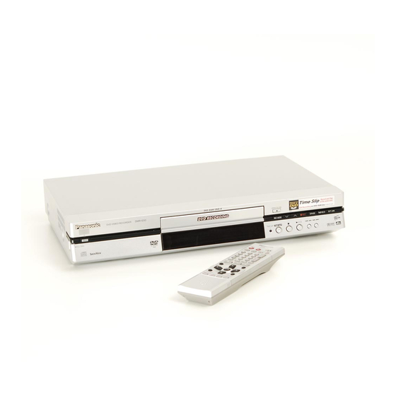
- Page 1 ORDER NO.DSD0302003C8 DVD Video Recorder DMR-E50EB DMR-E50EG DMR-E50GCS Colour (S).......Silver Type SPECIFICATIONS Specifications Power supply: AC220-240 V, 50 Hz (For E50EB/ EG) AC220-240 V, 50/ 60 Hz (For E50GCS) Power consumption: 29 W Recording system: DVD video recording standards (DVD-RAM),...
- Page 2 PAL I 75 ohm (For E50EB) PAL I 75 ohm terminated (For E50EB) PAL B/ G/ H 75 ohm terminated (For E50EG/ GCS) Channel Coverage: DMR-E50EB only UHF: CH 21-68 DMR-E50EG only VHF: CH E2-E12, A-H2 (For Italy) UHF: CH 21-69...
- Page 3 CH S01-S05 (S1-S3) CATV S1-S20 (M1-U10) S21-S41 [8MHz, RASTER] DMR-E50GCS only VHF: CH E2-E12 UHF: CH 21-69 CH S01-S05 CATV CH M1-M10 CH U1-U10 CH S21-S41 RF Converter UHF: CH21-68, 71 ± 3dB Output: 75 ohm (For the E50EB) Not provided (For the E50EG/ GCS) Video Video System:...
-
Page 4: Safety Precautions
Laser Power: No hazardous radiation is emitted with the safety protection Notes: Mass and dimensions shown are approximate. Specifications are subject to change without notice. Notes: The part of DVD RAM Drive (VXY1772) is listed separately. Please refer to ORDER NO. RAM0301002C0. 1. -
Page 5: Leakage Current Hot Check
Figure 1 1.1.2. LEAKAGE CURRENT HOT CHECK (See Figure 1 1. Plug the AC cord directly into the AC outlet. Do not use an isolation transformer for this check. 2. Connect a 1.5k , 10 watts resistor, in parallel with a 0.15 F capacitors, between each exposed metallic part on the set and a good earth ground such as a water pipe, as shown in... -
Page 6: Precaution Of Laser Diode
transistorsand semiconductor "chip" components. The following techniques should be used to help reduce the incidence of component damage caused by electro static discharge (ESD). 1. Immediately before handling any semiconductor component or semiconductor- equipped assembly, drain off any ESD on your body by touching a known earth ground. -
Page 7: How To Replace The Lithium Battery
( As shown in 16.2. The Main P.C.B. ) NOTE: The lithium battery is a critical component. ( Type No.: CR2354-1GUF Manufactured by Panasonic. ) It must never be subjected to excessive heat or discharge. It must therefore only be fitted in equipment designed specifically for its use. -
Page 8: Handling The Lead-Free Solder
5. Handling the Lead-free Solder 5.1. About lead free solder (PbF) Distinction of PbF P.C.B.: P.C.B.s (manufactured) using lead free solder will have a PbF stamp on the P.C.B. Caution:... -
Page 9: Service Explorer
Pb free solder has a higher melting point than standard solder; Typically the melting point is 50 - 70°F (30 - 40°C) higher. Please use a high temperature soldering iron. In case of the soldering iron with temperature control,please set it to 700 ± 20°F (370 ± 10°C). - Page 12 6.2. Service Explorer in Detail 6.2.1. Does not operate items needed: RAM drive, digital P.C.B., remote control. Conditions: Nothing special.
- Page 13 6.2.2. Poor Pictures Items needed: RAM drive, Digital P.C.B., RF cable, AV cable. Conditions: Check with TU IN-AV OUT(EE). When recording or playback is partially needed, follow the instructions.
- Page 15 6.2.3. Other Items needed: Digital P.C.B., HDD. Conditions: Nothing special.
-
Page 16: Standard Inspection Specifications After Making Repairs
Procedure Item to Check Turn on the power. The Panasonic RAM disc should be recognized. Enter the EE (TU IN / AV IN - AV OUT) mode. No abnormality should be seen in the picture, sound or operation. -
Page 17: Assembling And Disassembling
Item Contents Item Contents Check Block noise Distorted sound Crosscut noise noise (static, background noise, etc.) Dot noise The sound level is too low. Picture disruption The sound level is too high. Picture Sound Not bright enough The sound level changes. Too bright Flickering color Color fading... -
Page 18: The Top Cover
8.2. P.C.B. Positions 8.3. The Top Cover 1. Remove the 2 screws (A) and 3 screws (B). 2. Open the both ends at the front side of the Top cover a bit and lift the Top cover in the direction of the arrows. - Page 19 8.4. The Digital P.C.B. 1. Remove the FFC. CAUTION: When replacing Digital P.C.B., pay attention as below.
- Page 20 2. Remove the 2 screws. 3. Pinch the tab with the pliers to pull out the 3 Connectors and Digital P.C.B.
-
Page 21: The Front Panel
8.5. The Front panel 1. Remove the 2 connectors. - Page 22 2. Remove the 2 tab (A) and 3 tab (B) in this order. (The tab (A) and the tab (B) should be removed at the same time, respectively.) 3. Move the front panel to your side slowly and remove it.
- Page 23 8.6. The Front (L) and (R) P.C.B. 1. Remove the 2 screws and remove the Front Angle. 2. Remove the 4 screws (A) and remove the Front (R) P.C.B. 3. Remove the 2 screws (B) with Earth plate and remove the Front (L) P.C.B.
- Page 24 8.7. The DVD-RAM Drive 1. Remove the 4 screws. 2. Pull out the DVD-RAM Drive vertically and remove the connector.
-
Page 25: The Rear Panel
8.8. The Rear panel 1. Remove the Fan Motor connector. - Page 26 2. Remove the 8 screws (A) and a screw (B). 3. Remove the 2 tabs and remove the Rear panel.
- Page 27 8.8.1. In case of removing Fan motor from Rear panel 1. Remove a screw. 2. Push tip of rivet to remove it.
- Page 28 8.9. The Main Power Supply P.C.B. and Main P.C.B. 1. Remove the 2 connectors. 2. Remove the 3 screws (A) and 2 tab (A). 3. Remove the Main Power Supply P.C.B and tab (B), pull out it in the direction of the arrow.
-
Page 29: The Scart P.c.b
5. Remove the Main P.C.B. 8.10. The Scart P.C.B. 1. Pull out the Scart P.C.B. - Page 30 8.11. The RGB P.C.B. 1. Pull out the RGB P.C.B.
- Page 31 Note: Pull out the RGB and Scart P.C.B. after removing at a slant. 8.12. The VIF Decoder P.C.B. and Nicam/Decoder P.C.B.
-
Page 32: Service Positions
1. Remove the solder. 2. Pull out the VIF Decoder P.C.B. and Nicam/Decoder P.C.B. 9. Service Positions 9.1. Checking procedure Note: For the disassembling procedure, see the section 8. 9.2. Checking the Digital P.C.B., RGB P.C.B. and Scart P.C.B. 1. Remove the Top Cover. 2. - Page 33 4. Remove the Digital P.C.B. 5. Pull out the RGB P.C.B. 6. Use the extension cable (RFKZ0168) to connect the Main P.C.B. and Fan Motor. 7. Use the extension cable (RFKZ0164) to connect the Main P.C.B. and Digital P.C.B. 8. Use the extension FFC (RFKZ0125) to connect the RAM Drive and Digital P.C.B. 9.
- Page 34 1. Remove the Top Cover. 2. Remove the Front Panel. 3. Remove the Rear Panel. 4. Remove the Power Supply P.C.B., Main P.C.B. and RAM Drive. 5. Use the extension cable (RFKZ0168) to connect the Main P.C.B. and Fan Motor. 6.
- Page 35 9.4. Checking the Power Supply P.C.B. 1. Remove the Top Cover. 2. Remove the Front Panel. 3. Remove the screw which fixed Rear Panel and AC Inlet on the Power Supply P.C.B.. 4. Remove the Power Supply P.C.B., fix it on the insulation sheet. 5.
- Page 36 Service tools Extension Cable (Main P.C.B. - RFKZ0165 (20-pin) Front (L) P.C.B.) Extension Cable (Power supply RFKZ0166 (10-pin) P.C.B. - Front (R) P.C.B.) Extension Cable (Main P.C.B. - RFKZ0170 (19-pin) Power supply P.C.B.) Extension Cable (Main P.C.B. - RFKZ0171 (15-pin) Power supply P.C.B.) 10.
-
Page 37: Video Plus
Each buttons Functions name To turn power on or off on the DVD. VIDEO Plus+ To set timer program using G (Show View/G code/Show view/VIDEO Plus+ code) To set AV input on the TV. Numeric To put each number for buttons(10key) selecting each functions. - Page 38 <SEARCH> To set the cue or playback,playback 30seconds review during playback. previous by pressing the button. Below buttons are located inside slide cover. Each buttons Functions name REC MODE To set recording speed. F Rec To frexible recording with best quality to caluculate recording rate within remaining recording time.
- Page 39 Service mode setting: While the power is off, press TIME SLIP, STOP and OPEN / CLOSE simultaneously for five seconds. Item FL display Key operation Mode name Description Remote controller key Clear item Items 1-20 are cleared. [0] [0] while in service mode Error code display FL display of the last [0] [1] while in service mode...
- Page 40 Item FL display Key operation Mode name Description Remote controller key RTSC return XP (A& Disc recording of L1 Initialization mode (EE2/ [1] [3] while in service mode input Encoded and Interlace/ XP/ Audio decoded for external 48kHz) output without playback.
- Page 41 Item FL display Key operation Mode name Description Remote controller key Laser use time To check laser use [4] [1] while in service mode display time of drive Laser error count The number of times [4] [3] while in service mode that a laser error has occured due to a defective disc or...
- Page 42 Item FL display Key operation Mode name Description Remote controller key Front connection Press all the main [5] [4] while in service mode inspection unit’s buttons and check the connection with the Main P.C.B.. AV4-AV1 (RGB) Video signal at AV4 [8] [0] while in service mode SELECT should output with...
- Page 43 10.2.2. Other special modes Item FL display Key operation Mode name Description Remote controller key Main unit *All the main unit’s When the power is off, press initialization parameters are SKIP(R), TIME SLIP and OPEN/ initialized. CLOSE simultaneously for five seconds.
- Page 44 Diagnosis Description FL display Display Remote control Display appears when main unit and remote mode error controller modes are not matched. Abnormal inner Display appears when the drive temperature temperature exceeds 71Åé. Main unit is powered off detected forcibly. For 30 minutes after this, all key entries are disabled.
- Page 45 Diagnosis Description FL display Display Initialization error Display appears when initialization error is when main detected after starting up main microprocessor microprocessor for program recording. The is started up for event is saved in memory. program recording Remains displayed. Unsupported *A disc an unsupported format was played, UNSUPPORT disc error...
- Page 46 10.3.2. Error generating disk state 10.3.3. Disk production maker ID * Since a display is arbitrarily set up by the disk producer side, the above-mentioned display may be changed.
- Page 47 Please make it reference as an example of a display. 11. Abbreviations INITIAL/LOGO ABBREVIATIONS A0~UP ADDRESS ACLK AUDIO CLOCK AD0~UP ADDRESS BUS ADATA AUDIO PES PACKET DATA ADDRESS LATCH ENABLE AMUTE AUDIO MUTE AREQ AUDIO PES PACKET REQUEST AUDIO RF SERVO AMP INVERTED INPUT SERVO AMPOUTPUT ASYNC...
- Page 48 INITIAL/LOGO ABBREVIATIONS ERROR TORQUE CONTROL ERROR TORQUE CONTROL REFERENCE ENCODER SELECT ENCSEL EXTERNAL M CLOCK (81MHz/ ETMCLK 40.5MHz) ETSCLK EXTERNAL S CLOCK (54MHz) FBAL FOCUS BALANCE FCLK FRAME CLOCK FOCUS ERROR FOCUS ERROR AMP INVERTED INPUT FOCUS ERROR AMP OUTPUT FREQUENCY GENERATOR FREQUENCY SUB CARRIER FSCK...
- Page 49 INITIAL/LOGO ABBREVIATIONS READ ENABLE RFENV RF ENVELOPE RF PHASE DIFFERENCE OUTPUT (CD-ROM) REGISTER SELECT RSEL RF POLARITY SELECT RESET RESERVE SBI0, 1 SERIAL DATA INPUT SBO0 SERIAL DATA OUTPUT SBT0, 1 SERIAL CLOCK SERIAL DATA CLOCK SCKR AUDIO SERIAL CLOCK RECEIVER SERIAL CLOCK SCLK...
-
Page 50: Voltage And Waveform Chart
INITIAL/LOGO ABBREVIATIONS VBLANK V BLANKING COLLECTOR POWER SUPPLY VOLTAGE VCDCONT VIDEO CD CONTROL (TRACKING BALANCE) DRAIN POWER SUPPLY VOLTAGE VREF VIDEO FEED BACK VOLTAGE REFERENCE SOURCE POWER SUPPLYVOLTAGE WAIT BUS CYCLE WAIT WDCK WORD CLOCK WRITE ENABLE HIGH WORD SELECT RECEIVER X' TAL XALE X ADDRESS LATCH ENABLE... - Page 51 Therefore, there may exist some errors in the voltage values, depending on the internal impedance of the DC circuit tester. 12.1. Main Power Supply P.C.B. 12.2. Main P.C.B. 12.3. RGB P.C.B. 12.4. Scart P.C.B. 12.5. Nicam/Decoder P.C.B. 12.6. Front L P.C.B. 12.7.
- Page 52 IC102 Ref No. MODE 17.4 PLAY 17.5 STOP 17.3 IC301 IC302 Ref No. MODE 13.8 -0.1 14.7 -0.1 13.7 14.8 PLAY 13.9 -0.1 14.8 -0.1 13.6 14.8 STOP 13.9 -0.1 14.7 -0.1 13.6 14.7 Q101 Ref No. MODE PLAY STOP Ref No.
- Page 53 IC1501 IC1502 IC1504 Ref No. MODE PLAY STOP IC1505 IC1513 Ref No. MODE PLAY STOP IC3001 Ref No. MODE PLAY STOP IC3001 Ref No. MODE PLAY STOP IC3001 Ref No. MODE PLAY STOP IC3002 Ref No. MODE PLAY STOP IC3003 Ref No.
- Page 54 IC3004 Ref No. MODE PLAY STOP IC4001 Ref No. MODE PLAY STOP Ref No. IC4001 MODE PLAY STOP IC4005 IC4006 IC4007 Ref No. MODE PLAY STOP IC4009 IC4010 IC4011 Ref No. MODE 12.0 14.8 PLAY 12.0 14.8 12.0 STOP 12.0 14.5 12.0 IC4012...
- Page 55 IC7503 IC7504 IC7505 Ref No. MODE PLAY STOP IC7506 IC7507 Ref No. MODE 14.8 PLAY 14.8 STOP 14.5 IC7508 Ref No. MODE PLAY STOP Q3001 Q3002 Q3003 Q3004 Q3005 Ref No. MODE PLAY STOP Q3006 Q3007 Q3008 Q3009 Q3010 Ref No. MODE PLAY STOP...
- Page 56 IC3501 Ref No. MODE PLAY STOP IC3502 Ref No. MODE PLAY STOP IC3509 Ref No. MODE PLAY STOP Q3501 Q3502 Q3503 Q3504 Q3505 Ref No. MODE PLAY STOP Q3506 Q3507 Q3508 Q3509 Q3510 Ref No. MODE PLAY STOP...
- Page 57 IC3901 Ref No. MODE 12.0 PLAY 12.0 11.6 STOP 12.0 IC3901 Ref No. MODE PLAY STOP IC3901 Ref No. MODE PLAY STOP IC3902 Ref No. MODE PLAY STOP Q3901 Q3905 Q3906 Q3908 Q3909 Ref No. MODE -0.2 -0.1 PLAY -0.2 -0.4 STOP -0.3...
- Page 58 IC7301 Ref No. MODE PLAY STOP IC7301 Ref No. MODE PLAY STOP IC7301 Ref No. MODE PLAY STOP IC7302 Ref No. MODE PLAY STOP...
- Page 59 QR7001 Ref No. MODE PLAY STOP...
- Page 60 QR7801 Ref No. MODE PLAY STOP...
- Page 61 P9001 Ref No. MODE PLAY STOP P9001 Ref No. MODE PLAY STOP P9002 Ref No. MODE PLAY STOP P9002 Ref No. MODE PLAY STOP P9003 Ref No. MODE PLAY STOP Ref No. P9003 MODE PLAY STOP...
- Page 62 WF No . P9001-15 (REC/PLAY) WF No . P9001-16 (REC/PLAY) WF No. P9001-18 (REC/PLAY) (20usec/div) (20usec/div) (20usec/div) 0.6Vp-p 0.6Vp-p 0.6Vp-p WF No . P9001-20 (REC/PLAY) WF No . P9001-22 (REC/PLAY) WF No. P9001-28 (REC/PLAY) (20usec/div) (20usec/div) (20usec/div) 0.9Vp-p 1.0Vp-p 2.0Vp-p WF No.
-
Page 63: Block Diagram
12.8. P9001 Connector 12.9. P9001 Waveform 13. Block Diagram 13.1. Power Supply Block Diagram 13.1.1. Integrated Circuit Power Supply Chart (PSC 1 - PSC 19) 13.2. Analog Video Block Diagram 13.3. Analog Audio Block Diagram 13.4. Timer Block Diagram... - Page 64 X SW+5.15V PS105 PP1501 Q103 REG.D+12V REG.+12V (TO DVD RAM DRIVE) Q105 IC102 PHOTO SHUNT COUPLER REG. X SW+13V PS105 PP1501 Q107 REG.D+5V REG.+5V (TO DVD RAM DRIVE) Q104,Q106 DR P ON(H) PS105 PP1501 COLD DMR-E50EB/EG/GCS Power Supply Block Diagram...
- Page 65 IC7401 (REG.AU+12V) (REG.PS+12V) VOUT REG.AU+12V(PSC 4) VOUT PS+12V(PSC 16) ON(H) ON(H) POWER SAVE(H) FROM TIMER SEC. IC4013 QR4006,4007 (IC7502- (REG.AU+9V) VOUT REG.AU+9V(PSC 19) T7501 IP7501 (POWER TRANS.) UNREG+38V TO DU7402- DMR-E50EB/EG/GCS DMR-E50EB/EG/GCS Power Supply Block Diagram Power Supply Block Diagram...
- Page 66 PSC 1. X SW+5.15V PSC 9. REG.AU+5V Ref. No. Pin. No. Schematic Name Ref. No. Pin. No. Schematic Name IC7502 15,34,69 Timer (Main) IC4402 8 AV Input (Digital) 105,106,108 IC4403 IC50010 6 AV Decoder (Digital) IC7504 IC7506 PSC 10. REG.DAC+3.3V IC7508 Ref.
- Page 67 PSC 13. D+3.3V PSC 18.REG.D+5V Ref. No. Pin. No. Schematic Name Ref. No. Pin. No. Schematic Name IC3406 7,15,31,43 AV Encoder (Digital) IC4005 8 Audio Main (Main) 47,54,70,81 IC4006 88,91,99,106 IC4007 114,125,130 138,152,168 IC50001 1,11,14,19 AV Decoder (Digital) PSC 19.REG.AU+9V IC50002 1,3,9,14 Ref.
- Page 68 SCART Q3001,3002,FL3001 V OUT PP7401 PS3901 Y SEP.AND TUNER Y IN BUFFER SLICER VIDEO VIDEO SLICER 42 TO TIMER VIDEO (Q7505,Q7507) Q3003,3004,FL3002 DU7402 C SEP.AND C IN Y/C SEPA. BUFFER Q7402 TUNER VIDEO VIDEO OUT DMR-E50EB/EG/GCS Analog Video Block Diagram...
- Page 69 R CH IN TUNER L PK7302 PK7702 DECODER L PP7403 PS3903 DECODER L TUNER L DECODER L L CH IN AUDIO IN CH1(L) IC4007 IC4005 P9002 PP9702 IEC OUT FROM IC4006 DIGITAL OPTICAL D+5V (DIGITAL AUDIO OUT) DMR-E50EB/EG/GCS Analog Audio Block Diagram...
- Page 70 X7502 32.768MHz OPEN/CLOSE XCOUT S7816 IC7506 IC4001 (EEPROM) (AUDIO PROCESS) TIME-WARP TIME-WARP LED(H) P7801 P1104 P1103 PP1503 TIME-WARP XOUT LED(H) QR7801 X7503 D7801 (TIME-WARP LED DRIVE) X SW5.15V 10MHz IC3001 DU7402 (VIDEO PROCESS) VIF TUNER DMR-E50EB/EG/GCS FRONT(R)P.C.B. Timer Block Diagram...
- Page 71 Main Net Ref.No.9900 SERIES WORKING Digital P.C.B.connect circuit PP9701,PP9702,PP9703 MEMORY Main BUFFER MAIN CPU LOADER Video I/O Main Ref.No.3000 SERIES 16bit/128M- DMR-E50EB/EG/GCS 16bit/64M 16bit/64M P.C.B. SDRAM SDRAM SDRAM Audio Main Ref.No.4000 SERIES Digital Section Block Diagram Timer Ref.No.7500 SERIES IC50002...
- Page 72 IC Pin Terminal Chart IC Pin Terminal Chart IC3203 / VAD CON IC3402 / AV ENC IC3402/AV ENC IC3203/VAD CON IC50003/AV DEC IC6004 / MAIN CPU IC6002 / W-MEMORY IC3401/SDRAM(32bit/64M) SIGNAL NAME SIGNAL NAME SIGNAL NAME SIGNAL NAME Port Name Pin No Pin No Port Name...
-
Page 73: Signal Name
20-1 12-3 17-1 19-1 20-2 17-2 19-2 IC6004/MAIN CPU IC3406 / RTSC IC6701/GLUE IC6007 / BUFFER IC6006 / LOADER IC50003 / AVDEC IC6004 / MAIN CPU IC6701 / GLUE IC6006 / LOADER SIGNAL NAME SIGNAL NAME Pin No Port Name Pin No Port Name Pin No... -
Page 74: Schematic Diagram
13.5. Digital Section Block Diagram 13.5.1. Digital Block IC Pin Terminal Chart (TC 1 - TC 24) 14. Schematic Diagram 14.1. Interconnection Schematic Diagram 14.2. Main Power Supply Schematic Diagram (Main Power Supply P.C.B.) 14.3. Sub Power Supply Schematic Diagram (P) (Main P.C.B. 1/5) 14.4. -
Page 75: Interconnection Schematic Diagram
14 Schematic Diagram 14.1. Interconnection Schematic Diagram U/V TUNER P7001 P7501 PS3901 PP7401 DU7402 N SW 5V N SW 5V IIC CLK IIC CLK KEYIN2(L) KEYIN2(L) IIC DATA IIC DATA KEYIN2(R) KEYIN2(R) PROG PROG BOOSTER+B KEYIN3(L) KEYIN3(L) BOOSTER+5V BOOSTER+5 KEYIN3(R) KEYIN3(R) PS 5V PS 5V... -
Page 76: Dvd Ram Drive
AV-Encoder Ref.No.3400 SERIES Digital igital P.C.B.connect circuit PP9701,PP9702,PP9703 AV-Decoder Ref.No.50000 SERIES P.C.B. eo I/O Section Ref.No.3000/3900/4900 SERIES AV-Input Ref.No.3200/4400 SERIES dio Main Section Ref.No.4000 SERIES System Control Ref.No.6000 SERIES mer Section Ref.No.7500 SERIES Glue Ref.No.6700 SERIES DMR-E50EB/EG/GCS Interconnection Schematic Diagram... - Page 77 14.2. Main Power Supply Schematic Diagram (Main Power Supply P.C.B.) R1 22K R3 22K RD91EB R5 22K ETB28BF1L6A POWER TRANSFORMER C129 R162 R163 L118 EXCELSA24 100P 1SWB60 L101 EXCELSA24 D101 RL2ZLF C20 1000P C109 R27 220K R28 220K D7 AP01C 25V1000 L103 EXCELSA24 C103...
-
Page 78: Main Power Supply Schematic Diagram
10V220 R326 ZD303 C308 R341 C313 R333 3.32K MAZ8051 0.033 46.4K R321 R114 DMR-E50EB/EG/GCS ER SHOWN ON THIS DRAWING FOR ORDERRING.THE CORRECT PART NUMBER IS SHOWN Main Power Supply SLIGHTLY DIFFERNT OR AMENDED SINCE THIS DRAWING WAS PREPARED. Schematic Diagram... - Page 79 14.3. Sub Power Supply Schematic Diagram (P) (Main P.C.B. 1/5) TO P1102 MAIN POWER SUPPLY P.C.B. PP1501 LB1501 J0JHC0000032 D 1.8V D 1.8V LB1502 J0JHC0000032 D 3.3V D 3.3V LB1503 J0JHC0000032 X SW 5.15V LB1504 J0JHC0000032 X SW 5.9V LB1505 J0JHC0000032 X SW 13V P OFF(L) IC1501...
-
Page 80: Sub Power Supply Section (Main P.c.b. (1/5)) Schematic Diagram(P)
C1528 ANA 3.3V C1512 25V47 P OFF(L) DMR-E50EB/EG/GCS Sub Power Supply Section (Main P.C.B. (1/5)) NOTE:DO NOT USE THE PART NUMBER SHOWN ON THIS DRAWING FOR ORDERRING.THE CORRECT PART NUMBER IS SHOWN Schematic Diagram(P) IN THE PARTS LIST,AND MAY BE SLIGHTLY DIFFERNT OR AMENDED SINCE THIS DRAWING WAS PREPARED. - Page 81 14.4. Main Net Schematic Diagram (M) (Main P.C.B. 2/5) IC7401 C0DBZJG00005 (REG.PS +12V) X SW 13V C7401 R7402 10K 16V470 QR7404 X SW 5.9V UNR511400L D7401 R7405 470 MA2C165001VT (SWITCH) AV2 8 R7404 4700 C7439 R7403 R7401 10K 3900 Q7401 2SD1819AWL D7403 QR7402...
-
Page 82: Main Net Section(Main P.c.b. (2/5)) Schematic Diagram(M)
DGND COUT DM COUT DM DGND Y GCA CONT Y GCA CONT CLAMP DC CLAMP DC CLAMP PULSE CLAMP PULSE DGND V YIN DM V YIN DM DGND CPNCIN DM CPNCIN DM DMR-E50EB/EG/GCS Main Net Section(Main P.C.B. (2/5)) Schematic Diagram(M) - Page 83 R7409 270 R7414 100 RFC A OUT E50EB C7429 QR7406 3300P:E50B R7413 100 R7423 UNR211500L 0.1:E50EG/GCS 5.6K (MUTE) RFC A MUTE QR7407 UNR221500L (MUTE) IIC CLK IIC DATA PROG(H) CPS V OUT DMR-E50EB/EG/GCS Main Net Section(Main P.C.B. (2/5)) Schematic Diagram(M)
- Page 84 NIX R OUT 1 DECODER L DECODER L DECODER R DECODER R L3 IN L L3 IN L L3 IN R L3 IN R AUDIO MUTE AUDIO MUTE PWR SAVE(H) PWR SAVE(H) DMR-E50EB/EG/GCS .B. (2/5)) Main Net Section(Main P.C.B. (2/5)) Schematic Diagram(M)
- Page 85 14.5. Video I/O Schematic Diagram (V) (Main P.C.B. 3/5) JC REG5V CLAMP PULSE CLAMP DC Y GCA CONT ANA5V COUT DM LB3015 YOUT DM J0JHC0000032 LB3014 C3023 C3028 J0JHC0000032 0.01 0.01 C3019 D3001 0.01 R3061 MA2C165001VT C3068 15P A4 S IN L MIX L OUT2 C3070 6.3V47 R3026 1K...
-
Page 86: Video I/O Section(Main P.c.b. (3/5))Schematic Diagram(V)
R3038 C3018 C3020 R3059 0.01 6V100 FL3006 ELB4C083B R3049 Q3010 2SB1218A R3023 (AMP) R3039 wer Supply Section(Page: t Section(Page: R3060 O Section(Page: FL3007 ELB4C083B ain Section(Page: R3024 R3050 Q3011 2SB1218A ection(Page: (AMP) R3040 DMR-E50EB/EG/GCS Video I/O Section(Main P.C.B. (3/5))Schematic Diagram(V) -
Page 87: Video I/O Section(Main P.c.b. (3/5))Schematic Diagram
C0JBAR000292 (SELECTOR SW.) R3065 33K R3063 33K R3068 33K R3074 33K C3043 R3072 33K C3044 R3027 0 C3050 0.1 R3075 R3073 5600 5600 C3030 6V47 C3031 6V47 R3066 R3064 R3069 5600 5600 5600 DMR-E50EB/EG/GCS Video I/O Section(Main P.C.B. (3/5))Schematic Diagram(V) - Page 88 RGB IN(H) R3073 5600 AV2 V IN DMR-E50EB/EG/GCS Video I/O Section(Main P.C.B. (3/5)) NOTE:DO NOT USE THE PART NUMBER SHOWN ON THIS DRAWING FOR ORDERRING.THE CORRECT PART NUMBER IS SHOWN Schematic Diagram(V) IN THE PARTS LIST,AND MAY BE SLIGHTLY DIFFERNT OR AMENDED SINCE THIS DRAWING WAS PREPARED.
- Page 89 14.6. Audio Schematic Diagram (A) (Main P.C.B. 4/5) IP4001 D4FAR4000001 C4019 (VSF0015A04T) 16V10 R4022 C4031 C4027 R4021 50V1 50V1 C4021 16V10 R4023 R4015 L4002 R4039 ELESE220KA C4053 C4054 C4022 6.3V47 AADC L MIXLOUT DM L2 IN L L2 IN R C4069 0.1 MIXROUT DM R4099...
-
Page 90: Audio Main Section(Main P.c.b. (4/5)) Schematic Diagram(A)
C4070 C4072 10V220 10V220 DMR-E50EB/EG/GCS Audio Main Section(Main P.C.B. (4/5)) NOTE:DO NOT USE THE PART NUMBER SHOWN ON THIS DRAWING FOR ORDERRING.THE CORRECT PART NUMBER IS SHOWN Schematic Diagram(A) IN THE PARTS LIST,AND MAY BE SLIGHTLY DIFFERNT OR AMENDED SINCE THIS DRAWING WAS PREPARED. - Page 91 14.7. Timer Schematic Diagram (T) (Main P.C.B. 5/5) X SW 5.15V LB7511 ERJ3GEY0R00V X SW 5.9V C7606 C7605 6V47 LB7507 J0JGC0000020 VOUT D7513 B0JACE000001 IC7503 LB7510 J0JGC0000020 C0DBFHD00003 D7512 MA2C719 (REG.+5V) ON(H) LB7506 LB7508 C7583 R7598 C7581 C7580 J0JGC0000020 C7567 6V47 J0JGC0000020 6V220 6V100...
-
Page 92: Timer Section(Main P.c.b. (5/5))Schematic Diagram(T)
R7570 4700 IC7504 C0EBJ0000153 IC7505 (RESET) OUT VDD C0EBF0000182 QR7503 C7570 UNR521200L (INV.) C7571 R7532 C7572 C7608 R7595 0.01 IP7501 D4FAR4000001 LB7519 Q7516 ERJ3GEY0R00V 2SB0710A (INV.) QR7501 C7521 UNR521300L 16V220 R7574 (AV2 THROUGH(H) OUT) DMR-E50EB/EG/GCS Timer Section(Main P.C.B. (5/5))Schematic Diagram(T) - Page 93 MAZ4300NM R7510 C7523 0.047 C7587 D7505 R7515 R7516 C7528 MA2C18500E 3300 50V10 D7501 R7602 C7524 B0HAGR000005 0.01 R7601 Q7504 R7513 22K R7600 2SD0601A0L Q7503 (PWR SAVE(H):ON) R7511 2SD1994BR1VT (POWER CTL.) DMR-E50EB/EG/GCS NOTE:D Timer Section(Main P.C.B. (5/5)) Schematic Diagram(T) IN TH...
- Page 94 METER L METER R UNREG 38V DDGND DMR-E50EB/EG/GCS Timer Section(Main P.C.B. (5/5)) NOTE:DO NOT USE THE PART NUMBER SHOWN ON THIS DRAWING FOR ORDERING. THE CORRECT PART NUMBER IS SHOWN Schematic Diagram(T) IN THE PARTS LIST, AND MAY BE SLIGHTLY DIFFERNT OR AMENDED SINCE THIS DRAWING WAS PREPARED.
- Page 95 14.8. Digital Net Schematic Diagram (DN) (Digital P.C.B. 1/6) TO PP9701 MAIN P.C.B. (MAIN NET) P9001 CNPNCIN DM DGND V YIN DM DGND CLAMP PULSE CLAMP DC Y GCA CONT DGND COUT DM DGND YOUT DM DGND RPROUT DM DGND BPBOUT DM GPYOUT DM DGND...
- Page 96 (REG.SD+1.8V) C9004 UARTP2G UARTG2P DMR-E50EB/EG/GCS E:DO NOT USE THE PART NUMBER SHOWN ON THIS DRAWING FOR ORDERING. THE CORRECT Digital Net Section(Digital P.C.B.(1/6)) PART NUMBER IS SHOWN IN THE PARTS LIST,AND MAY BE SLIGHTLY DIFFERNT OR AMENDED SINCE THIS DRAWING WAS PREPARED.
- Page 97 14.9. AV Input Schematic Diagram (AI) (Digital P.C.B. 2/6) D3.3V D1.8V ANA 3.3V FL3213 F1H0J1050018 CLAMP PULSE CLAMP DC R3233 0 CPSVIN DM CPS(H) CL3205 R3220 R3223 6800 Q3202 Y GCA CONT 2SD1819A0L R3219 Q3201 (XVCO) 5600 2SB1218A C GCA CONT R3222 100K (XVCO)
- Page 98 2 4 6 8 RA3203 RA3204 D1H82204A024 D1H82204A024 LB3205 J0JHC0000032 C3208 IC3201 C3ABMG000103 (16bit/16M SDRAM) LB3202 LB3204 J0JHC0000032 J0JHC0000032 C3202 C3205 2 4 6 8 2 4 6 8 RA3201 RA3202 D1H82204A024 D1H82204A024 DMR-E50EB/EG/GCS AV Input Section(Digital P.C.B.(2/6)) Schematic Diagram(AI)
- Page 99 VDD(+1.8V) DT15 MODT15 DT14 MODT14 VSS3 DT13 MODT13 DT12 MODT12 VDD(+3.3V) DT11 MODT11 DT10 MODT10 VSS3 MODT9 MODT8 VDD(+3.3V) FL3212 F1H0J1050018 2 4 6 8 2 4 6 8 2 4 6 8 DMR-E50EB/EG/GCS AV Input Section(Digital P.C.B.(2/6)) Schematic Diagram(AI)
- Page 100 XAIOFCS 2 4 6 8 2 4 6 8 MRWR MRWW DMR-E50EB/EG/GCS AV Input Section (Digital P.C.B.(2/6)) NOTE:DO NOT USE ANY PART NUMBER SHOWN ON THIS SCHEMATIC DIAGRAM FOR ORDERING.WHEN YOU ORDER A PART,PLEASE REFER TO PARTS LIST. Schematic Diagram(AI)
- Page 101 14.10. AV Encoder Schematic Diagram (EN) (Digital P.C.B. 3/6) D3.3V D1.8V D GND MAA10 R3414 R3413 QR3403 UNR521300L FL3411 F1H0J1050018 (RESET(L) OUT) QR3402 UNR521300L XATRESET (XATRESET(H):ON) FL3410 F1H0J1050018 FL3428 F1H0J1050018 208 207 206 205 204 203 202 201 200 199 198 197 196 195 194 193 192 191 190 1 ANA3.3V CLK27A1 R656ENC0...
- Page 102 MDQA5 MN85572R MDQ5 MDQA4 (AV ENCODER) MDQ4 MDQA3 MDQ3 MDQA2 MDQ2 VDD(+3.3V) MDQA1 MDQ1 MDQA0 MDQ0 VDD(+1.8V) TEST5 HCIFZ RCKSEL1 VDD(+3.3V) DMACLK NHCS RCKSEL0 NHWE NHRE VDD(+1.8V) VDD(+3.3V) MSA4 MSA3 MSA2 MSA1 MSA5 DMR-E50EB/EG/GCS AV Encoder Section(Digital P.C.B.(3/6)) Schematic Diagram(EN)
- Page 103 SCMOD D1H82204A024 MINTEST STD7 STD6 ECCLK1 STD5 VDD(+3.3V) STD4 NCLKCNT STD7 STD6 RA3425 STD5 D1H82204A024 STD4 STD3 STD3 STD2 STD2 STD1 STD1 STD0 STD0 R3424 22 STCLK VDD(+3.3V) STVALID R3426 22 FL3418 F1H0J1050018 DMR-E50EB/EG/GCS AV Encoder Section(Digital P.C.B.(3/6)) Schematic Diagram(EN)
- Page 104 NCS1 VDD(+1.8V) VDD(+3.3V) MSD16 HMDT16 MSD17 HMDT17 MSD18 HMDT18 MSD19 HMDT19 MSD20 HMDT20 VDD(+3.3V) MSD21 HMDT21 MSD22 HMDT22 MSD23 HMDT23 MSD24 HMDT24 MSD25 HMDT25 MSD26 HMDT26 VDD(+3.3V) X3401 H2D400500001 40MHz OSC R3420 1M DMR-E50EB/EG/GCS AV Encoder Section(Digital P.C.B.(3/6)) Schematic Diagram(EN)
- Page 105 43 42 41 40 39 38 37 36 35 34 33 32 31 30 29 28 54 53 52 51 50 49 48 47 46 45 IC3403 C3ABQG000007 (128Mbit SDRAM) FL3412 FL3414 F1H0J1050018 F1H0J1050018 DMR-E50EB/EG/GCS AV Encoder Section(Digital P.C.B.(3/6)) Schematic Diagram(EN)
- Page 106 AD:AV Decoder Section(Page: C3ABQG000007 (16bit/128M SDRAM) S:System Control Section(Page: G:Glue Section(Page: NOTE: DO NOT USE ANY PART NUMBER SHOWN ON THIS SCHEMATIC DIAGRAM FOR ORDERING.WHEN YOU ORDER A PART,PLEASE REFER TO PARTS LIST. DMR-E50EB/EG/GCS AV Encoder Section(Digital P.C.B.(3/6)) Schematic Diagram(EN)
- Page 107 14.11. AV Decoder Schematic Diagram (AD) (Digital P.C.B. 4/6) D 3.3V D 1.5V D GND FL10 F1H0J1050018 1 3 5 7 1 3 5 7 MSA1 MSA2 MSA3 MSA4 MSA5 MSA6 MSA7 SA10 208 207 206 205 204 203 202 201 200 199 198 197 196 195 194 193 192 191 190 189 188 187 186 185 184 183 182 181 SA11 SA12 SA13...
- Page 108 DAC5OUT IREF1 2SB1218A AVDD3.3 COMP1 (BUFFER) DAC4OUT VREF DAC2OUT AVSS AVDD3.3 IREF2 COMP2 DAC1OUT PLLAVDD3.3 DAC3OUT PLLAVSS CL50006 FL17 F1H0J1050018 TCPOUT 2SB1218A (BUFFER) 1800 2SB1218A (BUFFER) 6V22 2SB1218A (BUFFER) J0JHC0000032 ANA3.3V D3.3V J-LINE DMR-E50EB/EG/GCS AV Decoder Section(Digital P.C.B.(4/6)) Schematic Diagram(AD)
- Page 109 CLK384FS F1H0J1050018 FL25 F1H0J1050018 AVDD DVDD C25 0.1 AVSS DVSS J0JGC0000 C26 16V10 XTALIN DVSS XTALOUT CLK512FS1 VSS2 CLK512FS2 VDD2 VDD2 IC10 C0FBBK000035 CLK33M VSS2 (AUDIO D/A CONVERTER) F1H0J1050018 J0JHC0000032 ANA3.3V D3.3V J-LINE DMR-E50EB/EG/GCS AV Decoder Section(Digital P.C.B.(4/6)) Schematic Diagram(AD)
- Page 110 FL21 F1H0J1050018 DAC 3.3V 6V100 ANA 3.3V DMR-E50EB/EG/GCS AV Decoder Section J-LINE (Digital P.C.B.(4/6)) NOTE:DO NOT USE THE PART NUMBER SHOWN ON THIS DRAWING FOR ORDERING. THE CORRECT PART NUMBER IS SHOWN IN THE PARTS LIST,AND MAY BE SLIGHTLY DIFFERNT OR AMENDED Schematic Diagram(AD) REF.NO.50000 SERIES...
- Page 111 14.12. System Control Schematic Diagram (S) (Digital P.C.B. 5/6) D 3.3V SD 1.8V XRESET DGND TO DIGITAL JIG P6001 FL6001 XDIAG F1H0J1050018 XDIAG XRESET SBIO MSORX D 3.3V SBO0 MSOTX 42 41 40 39 38 37 36 IC6002 C3ABQG000043 (WORKING MEMORY) XIRQ6 XIRQ6 XIRQ5...
- Page 112 8 6 4 2 8 6 4 2 8 6 4 2 8 6 4 2 DN:Digital Net Section(Page: AI:AV Input Section(Page: EN:AV Encoder Section(Page: AD:AV Decoder Section(Page: S:System Control Section(Page: G:Glue Section(Page: DMR-E50EB/EG/GCS System Control Section(Digital P.C.B.(5/6)) Schematic Diagram(S)
- Page 113 PIO10 XIRQ0 RX6004 XIRQ1 3300(X4) XIRQ2 R6008 XIRQ3 XIRQ4 XIRQ5 XIRQ6 R6009 XIRQ7 RX6005 XNMI 3300(X4) VDD(+3.3V) VDD(+1.8V) CKC95 CKC20 RX6007 33(X4) CKC69 CKC68 CKC67 CKC66 RX6008 33(X4) CKC65 CKC64 CKC63 CKC62 D3.3V DMR-E50EB/EG/GCS System Control Section(Digital P.C.B.(5/6)) Schematic Diagram(S)
- Page 114 SA22 MNZE0500YDR SA21 (MAIN CPU) SA20 SA19 SA18 SA17 SA16 VDD(+1.8V) VDD(+3.3V) SA15 SA14 SA13 SA12 SA11 SA10 VDD(+1.8V) VDD(+3.3V) SYSCLK R6014 R6013 R6021 D3.3V SD1.8V CL6001 R6010 R6011 R6015 R6022 X6001 H2D330500001 DMR-E50EB/EG/GCS System Control Section(Digital P.C.B.(5/6)) Schematic Diagram(S)
- Page 115 35 34 31 30 27 26 IC6006 C3CBKD000119 (LOADER) RX6019 33(X4) SD31 SD30 SD29 SD28 RX6017 33(X4) SD27 SD26 SD25 SD24 RX6016 33(X4) SD23 SD22 SD21 SD20 RX6015 33(X4) SD19 SD18 SD17 SD16 DMR-E50EB/EG/GCS System Control Section(Digital P.C.B.(5/6)) Schematic Diagram(S)
- Page 116 SA14 SA13 SA13 SA12 SA12 SA11 SA11 SA10 SA10 DMR-E50EB/EG/GCS System Control Section (Digital P.C.B.(5/6)) NOTE: DO NOT USE ANY PART NUMBER SHOWN ON THIS SCHEMATIC DIAGRAM Schematic Diagram(S) m(S) FOR ORDERING.WHEN YOU ORDER A PART,PLEASE REFER TO PARTS LIST.
- Page 117 14.13. Glue Schematic Diagram (G) (Digital P.C.B. 6/6) D3.3V DGND R6746 R6708 ENCMCK2 ENCMCK1 IC6702 C0JBAB000474 (CLOCK OUT) 104 103 102 101 100 99 98 97 96 95 94 93 92 91 90 89 88 87 86 85 84 83 82 81 FL6701 F1H0J1050018 FM21...
- Page 118 RX6733 D1H83334A024 2 4 6 8 7 5 3 1 2 4 6 8 2 4 6 8 7 5 3 1 7 5 3 1 7 5 3 1 7 5 3 1 DMR-E50EB/EG/GCS Glue Section(Digital P.C.B.(6/6)) Schematic Diagram(G)
- Page 119 RX6725 D1H84704A024 RX6724 D1H84704A024 R6722 CL6812 CL6813 R6724 RX6720 D1H81034A024 IC6703 REP3496A:E5 RX6714 REP3496C:E5 D1H81034A024 REP3496CD:E (DATA STRAGE) FL6702 F1H0J1050018 D3.3V CL6814 CL6811 CL6817 CL6816 RX6721 CL6815 D1H84704A024 R6723 47 DMR-E50EB/EG/GCS Glue Section(Digital P.C.B.(6/6)) Schematic Diagram(G)
- Page 120 MSD31 NOTE:DO NOT USE THE PART NUMBER SHOWN ON THIS DRAWING FOR ORDERING. THE CORRECT PART NUMBER IS SHOWN IN THE PARTS LIST, DMR-E50EB/EG/GCS AND MAY BE SLIGHTLY DIFFERNT OR AMENDED SINCE THIS DRAWING WAS PREPARED. Glue Section(Digital P.C.B.(6/6)) Schematic Diagram(G)
- Page 121 14.14. RGB Schematic Diagram TO PP3002 MAIN P.C.B. LB3501 (VIDEO I/O SEC.) J0JHC0000032 PS3502 PS 5V SCART V IN R3501 R3507 R3512 AV2 V IN R/C IN G IN C3501 C3502 C3503 Q3501 Q3502 Q3503 6V47 6V47 6V47 2SD0601A0L 2SD0601A0L 2SD0601A B IN (AMP)
- Page 122 2SB0709A (AMP) 3529 R3503 NOTE:DO NOT USE THE PART NUMBER SHOWN ON THIS DRAWING FOR ORDERRING.THE CORRECT PART NUMBER IS SHOWN DMR-E50EB/EG/GCS IN THE PARTS LIST,AND MAY BE SLIGHTLY DIFFERNT OR AMENDED SINCE THIS DRAWING WAS PREPARED. RGB Schematic Diagram...
-
Page 123: Scart Schematic Diagram
14.15. Scart Schematic Diagram TO PP7401 MAIN P.C.B. (MAIN NET SEC.) PS3901 IIC CLK IIC DATA PROG(H) R3908 R3909 BOOSTER+5V PS 5V TUNER VIDEO SCART V IN CPS V OUT C3910 C3911 16V10 16V10 CPN Y OUT PS 12V B OUT G OUT R/C OUT GAIN CTL... - Page 124 CLAMP INTERFACE 100K CONTROL3 CLAMP BLOCK CLAMP C3933 C3934 C3939 0.01 16V100 0.01 C3935 16V100 C3938 R3986 1200 73 10K C3930 0.01 72 10K R3975 R3976 R3985 R3910 4700 R3911 R3912 R3903 2200 2200 R3913 R3919 DMR-E50EB/EG/GCS Scart Schematic Diagram...
- Page 125 J0JGC0000020 C3901 C3902 0.01 6V47 IC3902 C9ZB00000282 (BUFFER) R3967 1500 Q3906 2SB0710A0L R3969 (AV1 PB(L):ON) 3300 R3902 R3968 QR3913 R3962 UNR521200L (RGB(H):ON) Q3905 2SD132800L (BLANKING OUT) R3901 QR3908 UNR521200L (BLANKING (L):OFF) DMR-E50EB/EG/GCS NOTE:DO NO Scart Schematic Diagram IN THE PA...
- Page 126 C3962 100P 100P DMR-E50EB/EG/GCS NOTE:DO NOT USE THE PART NUMBER SHOWN ON THIS DRAWING FOR ORDERING. THE CORRECT PART NUMBER IS SHOWN Scart Schematic Diagram IN THE PARTS LIST, AND MAY BE SLIGHTLY DIFFERNT OR AMENDED SINCE THIS DRAWING WAS PREPARED.
- Page 127 14.16. VIF Decoder Schematic Diagram R740 1K C724 C721 R717 E50EB:330P R727 E50EG/GCS:220P T701 C707 E50EB:EQV5EC083P 50V2.2 E50EG/GCS:EQV5EC082P R711 R745 3.3M C717 C708 C719 0.47 TRAP IC701 C1AA00000606 VIDEO CONT DEEMPHP D702 C704 C712 ERJ6GEY0R00V 0.033 R705 R708 4700 C701 C702 1000P C703...
- Page 128 HAVE THE SPECIAL CHARACTERISTICS FOR SAFETY. WHEN REPLACING ANY OF THESE COMPONENTS.ONLY THE SAME TYPE. NOTE: DMR-E50EB/EG/GCS DO NOT USE ANY PART NUMBER SHOWN ON THIS SCHEMATIC DIAGRAM VIF Decoder Schematic Diagram FOR ORDERING.WHEN YOU ORDER A PART,PLEASE REFER TO PARTS LIST.
-
Page 129: Nicam/Decoder Schematic Diagram
14.17. Nicam/Decoder Schematic Diagram C7335 C7305 6V100 IC7302 C0EAH0000051 TO PK7701 (RESET) MAIN P.C.B. (MAIN NET) PK7301 TU AUDIO IN LB7303 L7303 J0JCC0000021 G0C1R0JA0019 SW 5V C7303 C7306 C7334 6V100 0.01 50V2.2 C7311 100P R7304 C7301 R7301 C7302 ERJ3GEY0R00V TO PK7702 MAIN P.C.B. - Page 130 TL7303 R7309 R7314 TL7301 LB7302 C7313 C7312 J0JCC0000112 16V10 16V10 C7318 16V10 R7315 C7314 NOTE: DMR-E50EB/EG/GCS DO NOT USE ANY PART NUMBER SHOWN ON THIS SCHEMATIC DIAGRAM Nicam/Decoder Schematic Diagram FOR ORDERING.WHEN YOU ORDER A PART,PLEASE REFER TO PARTS LIST.
- Page 131 14.18. Front (L) Schematic Diagram TO P7501 MAIN P.C.B. (TIMER SECTION) P7001 CPN 2Y IN CPN 2C IN LINE 2V IN L2 C SDET L2 IN(L) L2 IN(R) POW LED KEYIN3(R) KEYIN3(L) KEYIN2(R) KEYIN2(L) < N SW 5V > N SW 5V POWER R7011 R7001...
- Page 132 (POWER LED DRIVE) NOTE:DO NOT USE THE PART NUMBER SHOWN ON THIS DRAWING FOR ORDERING. THE CORRECT PART NUMBER IS SHOWN IN THE PARTS LIST,AND MAY BE DMR-E50EB/EG/GCS SLIGHTLY DIFFERNT OR AMENDED SINCE THIS DRAWING WAS PREPARED. Front (L) Schematic Diagram...
- Page 133 14.6. Audio Schematic Diagram (A) (Main P.C.B. 4/5) 14.7. Timer Schematic Diagram (T) (Main P.C.B. 5/5) 14.8. Digital Net Schematic Diagram (DN) (Digital P.C.B. 1/6) 14.9. AV Input Schematic Diagram (AI) (Digital P.C.B. 2/6) 14.10. AV Encoder Schematic Diagram (EN) (Digital P.C.B. 3/6) 14.11.
- Page 134 14.12. System Control Schematic Diagram (S) (Digital P.C.B. 5/6) 14.13. Glue Schematic Diagram (G) (Digital P.C.B. 6/6) 14.14. RGB Schematic Diagram 14.15. Scart Schematic Diagram 14.16. VIF Decoder Schematic Diagram 14.17. Nicam/Decoder Schematic Diagram...
-
Page 135: Front (R) Schematic Diagram
14.18. Front (L) Schematic Diagram 14.19. Front (R) Schematic Diagram 15. Print Circuit Board 15.1. Main Power Supply P.C.B. 15.2. Main P.C.B. 15.2.1. Main P.C.B. (Section 1/4) 15.2.2. Main P.C.B. (Section 2/4) 15.2.3. Main P.C.B. (Section 3/4) 15.2.4. Main P.C.B. (Section 4/4) - Page 136 L118 Q101 C121 IP101 Q109 C116 L107 F101 D112 L113 D115 D116 C112 IP102 R140 JE15 JE16 Q103 L115 Q107 R A K JE10 Q108 JE11 VR102 JE12 PS105 PS102 Q104 Q105 Q106 Main Power Supply P.C.B. IC102 DMR-E50EB/EG/GCS (ETXMM444E4G)
- Page 137 Location Map (REAR) (FRONT) Main P.C.B. (1/4 Section) DMR-E50EB (REP3532B) DMR-E50EG/GCS (REP3532A)
- Page 138 Location Map (REAR) (FRONT) Main P.C.B. (2/4 Section) Main P.C.B. DMR-E50EG/GCS (REP3532A),DMR-E50EB (REP3532B) DMR-E50EB (REP3532B) DMR-E50EG/GCS (REP3532A)
- Page 139 MAIN P.C.B. Location Map (REAR) (FRONT) Main P.C.B. (3/4 Section) DMR-E50EB (REP3532B) DMR-E50EG/GCS (REP3532A)
- Page 140 (EB) (EB) (EB) (EG/GCS) Location Map (REAR) (FRONT) Main P.C.B. (4/4 Section) DMR-E50EB (REP3532B) DMR-E50EG/GCS (REP3532A)
- Page 141 MAIN P.C.B. QR7501 LB3002 C3026 C4063 C7545 R3026 R4022 R7529 Integrated Circuit IC1501 QR7502 LB3003 C3027 C4064 C7546 R3027 R4023 R7530 IC1502 QR7503 LB3004 C3028 C4065 C7547 R3028 R4024 R7531 IC1504 Test Point LB3011 C3029 C4067 C7548 R3029 R4027 R7532 IC1505 TL3001 LB3012...
- Page 142 DIGITAL P.C.B. OVER VIEW Digital P.C.B. (Component Side) (COMPONENT SIDE) DMR-E50EB (REP3496A), DMR-E50EG (REP3496C) DMR-E50GCS (REP3496CD)
- Page 143 DIGITAL P.C.B. OVER VIEW Digital P.C.B. (Foil Side) (FOIL SIDE) DMR-E50EB (REP3496A), DMR-E50EG (REP3496C) DMR-E50GCS (REP3496CD)
- Page 144 DIGITAL P.C.B. CKB21 F CKC131 F CL6785 F LB9020 F FL50025 F R3239 C R6742 F RA3414 C RX6048 Integrated Circuit IC3201 F CKB22 F CKC132 F CL6786 F LB9021 F FL50028 C R3240 C R6745 F RA3415 C RX6701 IC3203 C CKB23 F CKC133...
- Page 145 C3506 R3530 C3507 R3531 C3508 R3532 C3509 R3533 C3510 R3534 C3511 R3535 C3512 R3536 C3513 R3537 C3514 R3538 C3515 R3539 C3516 R3540 C3517 R3541 C3518 R3582 C3519 R3582 C3520 Adjustment C3521 VC3516 C3522 VC3517 C3523 VR3501 RGB P.C.B. DMR-E50EB/EG/GCS (REP3534A)
- Page 146 C LB3925 F C3920 F C3954 F R3910 F R3934 F R3984 JK3905 Capacitor C3921 C C3955 F R3911 F R3935 F R3985 ADDRESS INFORMATION C COMPONENT SIDE F FOIL SIDE SCART P.C.B. Scart P.C.B. (Component Side) (COMPONENT SIDE) DMR-E50EB/EG/GCS (REP3533A)
- Page 147 C LB3925 F C3920 F C3954 F R3910 F R3934 F R3984 JK3905 Capacitor C3921 C C3955 F R3911 F R3935 F R3985 ADDRESS INFORMATION C COMPONENT SIDE F FOIL SIDE SCART P.C.B. (FOIL SIDE) Scart P.C.B. (Foil Side) DMR-E50EB/EG/GCS (REP3533A)
- Page 148 VIF Decoder P.C.B. VIF Decoder P.C.B. VEP07A23Y: DMR-50EG/GCS VEP07A23Z: DMR-E50EB...
-
Page 149: Nicam/Decoder P.c.b
Nicam/Decoder P.C.B. Nicam/Decoder P.C.B. (VEP07A51A) DMR-50EB/EG/GCS... - Page 150 FRONT (L) P.C.B. DVD-E50EB/EG/GCS FRONT (L) P.C.B. (REP3528CB)
- Page 151 FRONT (R) P.C.B. DVD-E50EB/EG/GCS FRONT (R) P.C.B. (REP3528AA)
-
Page 152: Vif Decoder P.c.b
15.2.5. Main P.C.B. Address Information 15.3. Digital P.C.B. 15.3.1. Digital P.C.B. (Section 1/2) 15.3.2. Digital P.C.B. (Section 2/2) 15.3.3. Digital P.C.B. Address Information 15.4. RGB P.C.B. 15.5. Scart P.C.B. 15.5.1. Scart P.C.B. (Section 1/2) 15.5.2. Scart P.C.B. (Section 2/2) 15.6. VIF Decoder P.C.B. -
Page 153: Exploded Views
15.7. Nicam/Decoder P.C.B. 15.8. Front (L) P.C.B. 15.9. Front (R) P.C.B. 16. Exploded Views 16.1. Casing Parts & Mechanism Section 1 16.2. Casing Parts & Mechanism Section 2 16.3. Packing & Accessories Section 17. Replacement Parts List Notes: *Important safety notice: Components identified by mark have special characteristics important for safety. - Page 157 *Warning: This product uses a laser diode. Refer to caution statements. *Capacity values are in microfarads ( F) unless specified otherwise, P=Pico-farads (pF), F=Farads (F). *Resistance values are in ohms, unless specified otherwise, 1K=1,000 (OHM), 1M= 1,000k (OHM). *The marking (RTL) indicates the retention time is limited for this item. After the discontinuation of this assembly in production, it will no longer be available.
- Page 158 FRONT ORNAMENT(R) 20-11 RGK1622A-K FRONT ORNAMENT(L) 20-12 RKF0668-S TRAY DOOR 20-13 VMB3410 BLINDER SPRING 20-14 XTN2+6G SCREW 20-15 VGB0560 PANASONIC BADGE 20-16 RMC0539 DOOR SPRING 20-17 RGL0620-Q LIGHTING PIECE 20-18 RKF0666B-S PANEL DOOR (EG) 20-18 RKF0666C-S PANEL DOOR (EB) 20-18...
- Page 159 Ref. No. Part No. Part Name & Description Remarks C0701 ECJ2XF1C105Z 16V 1U ECJ2VF1C105Z (EB) C0702 ECJ1VB1H102K 50V 1000P (EB) C0703 ECJ2YB1A105K 10V 1U (EB) C0704 ECJ2VB1E333K 25V 0.033U (EB) C0707 ECEA1HKS2R2 50V 2.2U (EB) C0708 ECEA1HKAR47B 50V 0.47U (EB) C0710 ECJ1VF1H103Z 50V 0.01U...
- Page 160 Ref. No. Part No. Part Name & Description Remarks W502,03 ERJ8GEY0R00V 1/8W 0 (EB) W504 ERJ6GEY0R00V 1/10W 0 (EB) W506 ERJ8GEY0R00V 1/8W 0 (EB) W507-13 ERJ6GEY0R00V 1/10W 0 (EB) W514 ERJ8GEY0R00V 1/8W 0 (EB) W515 ERJ6GEY0R00V 1/10W 0 (EB) W516,17 ERJ8GEY0R00V 1/8W 0 (EB)
- Page 161 Ref. No. Part No. Part Name & Description Remarks R0725 ERJ6GEYJ101V 1/10W 100 (EG/GCS) R0727 ERJ3GEY0R00V 1/16W 0 (EG/GCS) R0729 ERJ3GEYJ103V 1/16W 10K D0GB103JA002 (EG/GCS) R0730 ERJ6GEYJ103V 1/10W 10K (EG/GCS) R0740 ERJ3GEYG102 1/16W 1K (EG/GCS) R0741 ERJ3GEYJ221V 1/16W 220 (EG/GCS) R0742 ERJ8GEYJ151V 1/8W 150...
- Page 162 Ref. No. Part No. Part Name & Description Remarks C3035-37 ECJ1VB1H103K 50V 0.01U (EB) C3038 ECEA1AKS221 10V 220U (EB) C3039 ECJ1VB1H103K 50V 0.01U (EB) C3040 ECEA0JKS101 6.3V 100U (EB) C3041 ECJ1VB1C104K 16V 0.1U (EB) C3042-44 ECEA0JKN470 6.3V 47U (EB) C3045 ECA0JM102 6.3V 1000U (EB)
- Page 163 Ref. No. Part No. Part Name & Description Remarks C4059 ECJ1VF1C104Z 16V 0.1U (EB) C4060 ECUV1H680JCG 50V 68P ECJ2VC1H680J (EB) C4061 ECJ1VF1C104Z 16V 0.1U (EB) C4062 ECA1AM221 10V 220U (EB) C4063,64 F2A1C4700011 16V 47U (EB) C4065 ECJ1VF1C104Z 16V 0.1U (EB) C4067 F2A0J470A179 6.3V 47U...
- Page 164 Ref. No. Part No. Part Name & Description Remarks C7535 ECJ1VB1C104K 16V 0.1U (EB) C7536 ECEA0JKS101 6.3V 100U (EB) C7537 ECJ1VF1C104Z 16V 0.1U (EB) C7538 ECJ1VB1C104K 16V 0.1U (EB) C7539 ECUV1H200JCV 50V 20P ECJ1VC1H200J (EB) C7540 ECJ1VC1H151J 50V 150P (EB) C7541 ECJ1VC1H101J 50V 100P...
- Page 165 Ref. No. Part No. Part Name & Description Remarks D3001 MA2C165001VT DIODE (EB) D4001 MA2C165001VT DIODE (EB) D4005,06 MA3Z142D0RG DIODE (EB) D7401 MA2C165001VT DIODE (EB) D7402 MA4300N-M DIODE MAZ4300NM (EB) D7403 MA2C165001VT DIODE (EB) D7501 VSD0002 DIODE B0HAGR000005 (EB) D7502 ERA22-02 DIODE B0HAGM000001 (EB)
- Page 166 Ref. No. Part No. Part Name & Description Remarks IP7501 D4FAR4000001 IC PROTECTOR (EB) JK3001 K1U822B00001 JACK,AV IN/OUT (EB) L3006,07 G0C4R7JA0019 COIL 4.7UH (EB) L4002 ELESE220KA COIL 22UH (EB) L7402 VLQ0599J270 COIL 27UH G0C270JA0026 (EB) L7403 VLQ0599J2R2 COIL 2.2UH G0C2R2JA0026 (EB) LB1501-05 J0JHC0000032 COIL...
- Page 167 Ref. No. Part No. Part Name & Description Remarks Q7509 2SC2295 TRANSISTOR (EB) Q7510 2SB709A TRANSISTOR 2SB0709A (EB) Q7511,12 2SD0601A0L TRANSISTOR (EB) Q7513 2SD1819A0L TRANSISTOR (EB) Q7515 2SD1119-R TRANSISTOR 2SD11190R (EB) Q7516 2SB710A TRANSISTOR 2SB0710A (EB) QR4001-07 UNR521100L TRANSISTOR (EB) QR4012 UN5113TW TRANSISTOR...
- Page 168 Ref. No. Part No. Part Name & Description Remarks R3068 ERJ3RBD333V 1/16W 33K (EB) R3069 ERJ3RBD562V 1/16W 5.6K (EB) R3070 ERJ3RBD333V 1/16W 33K (EB) R3071 ERJ3RBD562V 1/16W 5.6K (EB) R3072 ERJ3RBD333V 1/16W 33K (EB) R3073 ERJ3RBD562V 1/16W 5.6K (EB) R3074 ERJ3RBD333V 1/16W 33K (EB)
- Page 169 Ref. No. Part No. Part Name & Description Remarks R7401,02 ERJ3GEYJ103V 1/16W 10K D0GB103JA002 (EB) R7403 ERJ3GEYJ392V 1/16W 3.9K (EB) R7404 ERJ3GEYJ472V 1/16W 4.7K (EB) R7405 ERDS2FJ471 1/4W 470 (EB) R7406 ERJ3GEYJ223V 1/16W 22K D0GB223JA002 (EB) R7407 ERJ3GEYJ103V 1/16W 10K D0GB103JA002 (EB) R7408 ERJ3GEYD153V...
- Page 170 Ref. No. Part No. Part Name & Description Remarks R7543 ERJ3GEYJ104 1/16W 100K (EB) R7544 ERJ3GEYJ101 1/16W 100 D0GB101JA002 (EB) R7545 ERJ3GEYJ103V 1/16W 10K D0GB103JA002 (EB) R7546 ERJ3GEYJ472V 1/16W 4.7K (EB) R7547 ERJ3GEYJ223V 1/16W 22K D0GB223JA002 (EB) R7548 ERJ3GEY0R00V 1/16W 0 (EB) R7549 ERJ3GEYJ332V...
- Page 171 Ref. No. Part No. Part Name & Description Remarks REP3532A C1502 F2A1E221A210 25V 220U (EG/GCS) C1503,04 F2A1A471A211 10V 470U (EG/GCS) C1505,06 F2A0J471A256 6.3V 470U (EG/GCS) C1508,09 F2A0J470A012 6.3V 47U (EG/GCS) C1512 F2A1E4700048 25V 47U (EG/GCS) C1514 F2A0J470A012 6.3V 47U (EG/GCS) C1528 ECJ1VB1C104K 16V 0.1U...
- Page 172 Ref. No. Part No. Part Name & Description Remarks C4003,04 ECJ1VB1H103K 50V 0.01U (EG/GCS) C4005-07 F2A1H1R0A236 50V 1U (EG/GCS) C4008 F2A1C221A019 16V 220U (EG/GCS) C4010 F2A1H1R0A236 50V 1U (EG/GCS) C4011 F2A1H100A236 50V 10U (EG/GCS) C4012 ECJ2VB1E104K 25V 0.1U (EG/GCS) C4013 F2A1H1R0A236 50V 1U (EG/GCS)
- Page 173 Ref. No. Part No. Part Name & Description Remarks C7317 ECEA1CKA470 16V 47U (EG/GCS) C7318 ECEA1CKS100 16V 10U (EG/GCS) C7323 ECJ1VC1H102J 50V 1000P (EG/GCS) C7324 ECJ1VF1C104Z 16V 0.1U (EG/GCS) C7329 ERJ3GEY0R00V 1/16W 0 (EG/GCS) C7330 ERJ3GEYJ822V 1/16W 8.2K D0GB822JA002 (EG/GCS) C7332 ECJ1VF1C104Z 16V 0.1U...
- Page 174 Ref. No. Part No. Part Name & Description Remarks C7540 ECJ1VC1H151J 50V 150P (EG/GCS) C7541 ECJ1VC1H101J 50V 100P (EG/GCS) C7542 ECJ1VB1C104K 16V 0.1U (EG/GCS) C7543 ECEA0JKS470 6.3V 47U (EG/GCS) C7544,45 ECJ1VF1C104Z 16V 0.1U (EG/GCS) C7546 ECJ1VB1C104K 16V 0.1U (EG/GCS) C7547 ECEA0JKS470 6.3V 47U (EG/GCS)
-
Page 175: Tuner Pack
Ref. No. Part No. Part Name & Description Remarks D7402 MA4300N-M DIODE MAZ4300NM (EG/GCS) D7403 MA2C165001VT DIODE (EG/GCS) D7501 VSD0002 DIODE B0HAGR000005 (EG/GCS) D7502 ERA22-02 DIODE B0HAGM000001 (EG/GCS) D7503 MAZ4240NMF DIODE (EG/GCS) D7504,05 MA2C18500E DIODE (EG/GCS) D7506 MA4300N-M DIODE MAZ4300NM (EG/GCS) D7507 B0ACCK000005 DIODE... - Page 176 Ref. No. Part No. Part Name & Description Remarks K7301-03 ERJ3GEY0R00V 1/16W 0 (EG/GCS) K7305 ERJ3GEY0R00V 1/16W 0 (EG/GCS) L3006,07 G0C4R7JA0019 COIL 4.7UH (EG/GCS) L4002 ELESE220KA COIL 22UH (EG/GCS) L7303 G0C1R0JA0019 COIL (EG/GCS) L7403 VLQ0599J2R2 COIL 2.2UH G0C2R2JA0026 (EG/GCS) LB1501-05 J0JHC0000032 COIL (EG/GCS)
- Page 177 Ref. No. Part No. Part Name & Description Remarks Q7505 2SB709A TRANSISTOR 2SB0709A (EG/GCS) Q7506 2SD1819A0L TRANSISTOR (EG/GCS) Q7507 2SB709A TRANSISTOR 2SB0709A (EG/GCS) Q7508 2SD1819A0L TRANSISTOR (EG/GCS) Q7509 2SC2295 TRANSISTOR (EG/GCS) Q7510 2SB709A TRANSISTOR 2SB0709A (EG/GCS) Q7511,12 2SD0601A0L TRANSISTOR (EG/GCS) Q7513 2SD1819A0L TRANSISTOR...
- Page 178 Ref. No. Part No. Part Name & Description Remarks R3066 ERJ3RBD562V 1/16W 5.6K (EG/GCS) R3067 ERJ3GEY0R00V 1/16W 0 (EG/GCS) R3068 ERJ3RBD333V 1/16W 33K (EG/GCS) R3069 ERJ3RBD562V 1/16W 5.6K (EG/GCS) R3070 ERJ3RBD333V 1/16W 33K (EG/GCS) R3071 ERJ3RBD562V 1/16W 5.6K (EG/GCS) R3072 ERJ3RBD333V 1/16W 33K (EG/GCS)
- Page 179 Ref. No. Part No. Part Name & Description Remarks R4093 ERJ3GEYJ221V 1/16W 220 (EG/GCS) R4099 ERJ3GEYJ101 1/16W 100 D0GB101JA002 (EG/GCS) R7301 ERJ3GEY0R00V 1/16W 0 (EG/GCS) R7304 ERJ3GEYJ101 1/16W 100 D0GB101JA002 (EG/GCS) R7307 ERJ3GEY0R00V 1/16W 0 (EG/GCS) R7309 ERJ3GEYJ103V 1/16W 10K D0GB103JA002 (EG/GCS) R7311 ERJ3GEYJ221V...
- Page 180 Ref. No. Part No. Part Name & Description Remarks R7532 ERJ3GEYD153V 1/16W 15K D0HB153ZA002 (EG/GCS) R7533,34 ERJ3GEYJ472V 1/16W 4.7K (EG/GCS) R7535 ERJ3GEYJ223V 1/16W 22K D0GB223JA002 (EG/GCS) R7536 ERJ3GEYJ472V 1/16W 4.7K (EG/GCS) R7537 ERJ3GEYJ473V 1/16W 47K D0GB473JA002 (EG/GCS) R7538 ERJ3GEYJ273V 1/16W 27K D0GB273JA002 (EG/GCS) R7539 ERJ3GEYJ225V...
- Page 181 Ref. No. Part No. Part Name & Description Remarks W522-27 ERJ3GEY0R00V 1/16W 0 (EG/GCS) W528 ERJ6GEY0R00V 1/10W 0 (EG/GCS) W529-31 ERJ3GEY0R00V 1/16W 0 (EG/GCS) X7301 H0D245500016 CRYSTAL OSCILLATOR (EG/GCS) X7501 H0D443400035 CRYSTAL OSCILLATOR (EG/GCS) X7502 H0A327200064 CRYSTAL OSCILLATOR (EG/GCS) X7503 VSX1043-T CRYSTAL OSCILLATOR H0D100500006 (EG/GCS)
-
Page 182: Crystal Oscillator
Ref. No. Part No. Part Name & Description Remarks R7322 ERJ3GEY0R00V 1/16W 0 R7324,25 ERJ3GEYJ101 1/16W 100 D0GB101JA002 W6,W7 ERJ3GEY0R00V 1/16W 0 X7301 H0D245500016 CRYSTAL OSCILLATOR REP3496A/REP3496C/REP3496CD C3202 ECJ1VB1C104K 16V 0.1U C3203 ECJ1VB1H222K 50V 2200P C3205 ECJ1VB1C104K 16V 0.1U C3207 ECJ1VB1H103K 50V 0.01U C3208... - Page 183 Ref. No. Part No. Part Name & Description Remarks FL3205-09 F1H0J1050018 FILTER FL3212,13 F1H0J1050018 FILTER FL3216 F1H0J1050018 FILTER FL3218 F1H0J1050018 FILTER FL3220 F1H0J1050018 FILTER FL3225 F1H0J1050018 FILTER FL3401-06 F1H0J1050018 FILTER FL3409-19 F1H0J1050018 FILTER FL3421,22 F1H0J1050018 FILTER FL3425 F1H0J1050018 FILTER FL3428 F1H0J1050018 FILTER FL4401...
- Page 184 Ref. No. Part No. Part Name & Description Remarks IC50013 C0JBAD000107 IC50014 C0JBAF000206 IC50015 C0CBCBD00002 LB3202-05 J0JHC0000032 COIL LB3401,02 J0JHC0000032 COIL LB4402,03 J0JGC0000020 COIL LB9001 J0JHC0000032 COIL LB9003 J0JHC0000045 COIL LB9005 J0JHC0000032 COIL LB9006 J0JHC0000045 COIL LB9009 J0JHC0000032 COIL LB9012 J0JHC0000045 COIL LB9013-16...
- Page 185 Ref. No. Part No. Part Name & Description Remarks R3409 ERJ3GEYJ102V 1/16W 1K R3410 ERJ3GEYJ562V 1/16W 5.6K D0GB562JA002 R3411 ERJ3GEYJ103V 1/16W 10K D0GB103JA002 R3412 ERJ3GEYJ332V 1/16W 3.3K D0GB332JA002 R3413,14 ERJ3GEYJ103V 1/16W 10K D0GB103JA002 R3415,16 ERJ3GEYJ220V 1/16W 22 R3419 ERJ3GEYJ220V 1/16W 22 R3420 ERJ3GEYJ105V 1/16W 1M...
- Page 186 Ref. No. Part No. Part Name & Description Remarks R50007 ERJ3GEYJ220V 1/16W 22 R50008-10 ERJ3GEYJ470V 1/16W 47 R50012 ERJ3GEY0R00V 1/16W 0 R50013 ERJ3RBD273V 1/16W 27K R50014 ERJ3GEYJ820V 1/16W 82 R50015 ERJ3RBD153 1/16W 15K R50017 ERJ3GEYJ390 1/16W 39 R50018 ERJ3GEY0R00V 1/16W 0 R50021 ERJ3GEYJ220V 1/16W 22...
-
Page 187: Remote Sensor
Ref. No. Part No. Part Name & Description Remarks RX6009-12 D1H84704A024 RESISTOR-RESISTOR RX6013-17 D1H83304A024 RESISTOR-RESISTOR RX6018 D1H84704A024 RESISTOR-RESISTOR RX6019 D1H83304A024 RESISTOR-RESISTOR RX6020 D1H84704A024 RESISTOR-RESISTOR RX6021 D1H83304A024 RESISTOR-RESISTOR RX6022 D1H84704A024 RESISTOR-RESISTOR RX6025 D1H83304A024 RESISTOR-RESISTOR RX6026 D1H84704A024 RESISTOR-RESISTOR RX6027 D1H81034A024 RESISTOR-RESISTOR RX6030-33 D1H84704A024 RESISTOR-RESISTOR RX6034-48... - Page 188 Ref. No. Part No. Part Name & Description Remarks P7001 K1KA20B00132 CONNECTOR(20P) QR7001 UN2214TX TRANSISTOR UNR221400L R7001 ERDS2FJ391 1/4W 390 R7002 ERJ3GEYJ102V 1/16W 1K R7008-10 ERJ3GEYJ750 1/16W 75 R7011 ERDS2FJ330 1/4W 33 S7003 EVQ11G07K SWITCH REP3528AA D7801 B3ABA0000396 DIODE P7801 K1KA10B00196 CONNECTOR(10P) QR7801...
- Page 189 Ref. No. Part No. Part Name & Description Remarks C3925 ECJ1VB1H103K 50V 0.01U C3928,29 ECA1HAK010XI 50V 1U C3930 ECJ1VB1H103K 50V 0.01U C3931,32 ECA1HAK010XI 50V 1U C3933 ECA1CAK101XB 16V 100U C3934 ECJ1VB1H103K 50V 0.01U C3935 ECA1CAK101XB 16V 100U C3938 ECJ1VF1C104Z 16V 0.1U C3939 ECJ1VB1H103K 50V 0.01U...
- Page 190 Ref. No. Part No. Part Name & Description Remarks R3913 ERJ3RBD181V 1/16W 180 R3914 ERJ3RBD151 1/16W 150 R3919 ERJ3RBD151 1/16W 150 R3921 ERJ6GEYG750 1/10W 75 R3922,23 ERJ6GEYJ471V 1/10W 470 R3924 ERDS2FJ471 1/4W 470 R3925-28 ERJ6GEYG750 1/10W 75 R3929,30 ERJ6GEYJ471V 1/10W 470 R3931-33 ERJ3RED750V 1/16W 75...
- Page 191 Ref. No. Part No. Part Name & Description Remarks FL3501 ELB4E042B FILTER IC3501 C1AB00000773 IC3502 C0JBAR000292 IC3509 C1AA00000016 L3502 G0C100JA0019 COIL 10UH LB3501,02 J0JHC0000032 COIL PS3501 VJS3042F008W CONNECTOR(8P) K1KB08B00028 PS3502 VJS3042F012W CONNECTOR(12P) K1KB12B00030 Q3501-04 2SD0601A0L TRANSISTOR Q3505 2SC2295 TRANSISTOR Q3506 2SA10220BL TRANSISTOR Q3507,08...
- Page 192 Ref. No. Part No. Part Name & Description Remarks VC3516,17 ECRLA030E53R VR3501 EVMECSA00B53 X3501 H0D443400037 CRYSTAL OSCILLATOR ETXMM444E4G C001 KH101K 100P C002 KH102M 1000P C003,04 ECQU2A224ML 0.22U C005 KH101K 100P C006-08 KH102M 1000P C009 KMM2W470JZ 450V 47U C010-12 MBB105K1 16V 1U C013 MBC102J5 50V 1000P...
- Page 193 Ref. No. Part No. Part Name & Description Remarks C316 MBB224K2 25V 0.22U D001 1SWB60 DIODE D002 1SS355 DIODE B0ACCK000005 D004 1SS355 DIODE B0ACCK000005 D006 M1FL20U DIODE D007 AP01C DIODE B0HADV000010 D008 AL01Z DIODE B0HAMM000077 D101 RL2ZLF DIODE B0HANM000021 D103 RK46 DIODE B0JAPG000009...
- Page 194 Ref. No. Part No. Part Name & Description Remarks Q004 UN2213 TRANSISTOR UNR2213 Q101 2SB709A TRANSISTOR 2SB0709A Q102 2SD601A-R TRANSISTOR 2SD0601AR Q103 UPA1717G TRANSISTOR Q104 2SD601A-R TRANSISTOR 2SD0601AR Q105 UN221L TRANSISTOR UNR221L Q106 UN2111 TRANSISTOR UNR2111 Q107 UPA1720G TRANSISTOR Q108 2SB766A TRANSISTOR 2SB0766A...
- Page 195 Ref. No. Part No. Part Name & Description Remarks R128 CR10J561 0.1W 560 R129 CR10J101 0.1W 100 R130 ERDS2FJ121 0.25W 120 R131 CR10J102 0.1W 1K R132 CR10J471 0.1W 470 R133,34 CR10J682 0.1W 6.8K R135 ER0S2TKF1430 0.25W 14K R136 CR10J822 0.1W 8.2K R137 CR10J102 0.1W 1K...
- Page 196 Ref. No. Part No. Part Name & Description Remarks R343 CR10J102 0.1W 1K R344,45 CR10J103 0.1W 10K T001 ETB28BF1L6A TRANSFORMER TH001 NC21F104J THERMISTOR VR102 EVMEASA01B52 V.R. Z002 ERZVGAD471 VARISTOR ZD001 RD91EB DIODE ZD002 MA8270 DIODE ZD101 MA8039 DIODE ZD102 MA8027 DIODE ZD103 MA4075N...