
Related Manuals for Panasonic DMR-E53EG


Summary of Contents for Panasonic DMR-E53EG
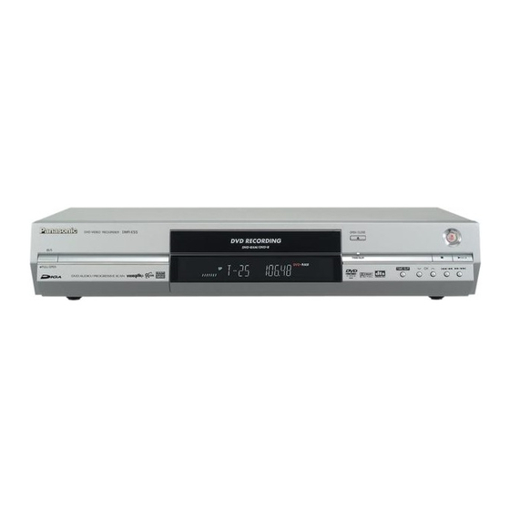
- Page 1 ORDER NO.DSD0403001C8 DVD Video Recorder DMR-E53EG / DMR-E55EB / DMR-E55EG / DMR-E55EBL / DMR-E55EP Colour (K).......Black Type (S).......Silver Type SPECIFICATIONS...
- Page 2 1. Safety precautions 1.1. General guidelines 1. When servicing, observe the original lead dress. If a short circuit is found, replace all parts which have been overheated or...
- Page 3 damaged by the short circuit. 2. After servicing, see to it that all the protective devices such as insulation barriers, insulation papers shields are properly installed. 3. After servicing, make the following leakage current checks to prevent the customer from being exposed to shock hazards. 1.1.1.
- Page 4 6. The potential at any point should not exceed 0.75 volts RMS. A leakage current tester (Simpson Model 229 or equivalent) may be used to make the hot checks, leakage current must not exceed 1/2 milliampere. In case a measurement isoutside of the limits specified, there is a possibility of a shock hazard, and the equipment should be repaired and rechecked before it is returned to the customer.
- Page 5 comparableconductive material). 7. Immediately before removing the protective material from the leads of a replacement ES device, touch the protective material to the chassis or circuit assembly into which the device will be installed. Caution Be sure no power is applied to the chassis or circuit, and observe all other safety precautions.
- Page 6 4.1. About lead free solder (PbF) Distinction of PbF P.C.B.: P.C.B.s (manufactured) using lead free solder will have a PbF stamp on the P.C.B. Caution: - Pb free solder has a higher melting point than standard solder; Typically the melting point is 50 - 70°F (30 - 40°C) higher. Please use a high temperature soldering iron.
- Page 7 direction of Arrow. 6. Put the Upper Base Unit so that the Opener Roller is inserted into the groove. 7. Check center of Opener Roller is seen through the Opener position Checking Hole, and tighten 4 screws. 7. Service Explorer Confirm “RAM-Drive Last Error”...
- Page 8 *After finishing display “(7). Factor of Drive Error occurring”, press [0] [2] ~[9] [9] keys of the Remote Controller so that 99 memories can be displayed as maximum. 2. Press [4] [2] keys of remote controller. Example of FL Display: (1) Error Number is displayed for 5 seconds.
- Page 9 FL Display (Disc Disc Maker Country Maker's ID) Panasonic Japan Pioneer Japan Mitsubishi Chemical Japan Corporation Japan Maxell Japan MITUI CHEMICALS Japan Victor JVC Japan TAIYOYUDEN Taiyo yuden Japan Giga Storage Taiwan PRODISC Prodisc Taiwan PRINCO PRINCO Taiwan RITEK RITEK...
- Page 10 FL Display Disc Type DVD-ROM/Video Audio-CD 2.6GB DVD-RAM 4.7GB DVD-RAM DVD-R Error Occurring Disc State 8. Self-Diagnosis and Special Mode Setting 8.1. Self-Diagnosis Functions Self-Diagnosis Function provides information for errors to service personnel by “Self-Diagnosis Display” when any error has occurred. U14, H** and F** are stored in memory and held.
- Page 11 Error Diagnosis contents Description Monitor FL display Display Code Remote control code Display appears when main unit No display error and remote controller codes are not matched. “*” is remote controller code of the main Display for 5 seconds. Abnormal inner Display appears when the drive No display temperature detected...
- Page 12 Error Diagnosis contents Description Monitor FL display Display Code Unsupported disc error *An unsupported format disc was “This disc is UNSUPPORT played, although the drive starts incompatible.” normally. *The data format is not Display for 5 seconds. supported, although the media type is supported.
- Page 13 Item FL display Key operation Mode name Description Front Key TEST Mode *All the main unit's parameters Press [SKIP (REV)], (include tuner) are initialized. SLIP] and [OPEN keys simultaneously five seconds when is off. Service Mode Setting every kind of modes for When the power servicing.
- Page 14 Item FL display Key operation Mode name Description Front Key Aging Perform sequence of modes as * Display following the then When the power Aging Description shown below mode. press [CH DOWN], continually. SLIP] and [OPEN simultaneously for five seconds and than 10 seconds.
- Page 15 Item FL display Key operation Mode name Description Front Key Progressive The progressive setting is The display before When the power initialization initialized to Interlace. execution leaves. mode), press [STOP] [TIME SLIP] simultaneously for seconds. Aging Contents (Example): 8.3. Service Modes Service mode setting: While the power is off, press TIME SLIP, STOP and OPEN / CLOSE simultaneously for five seconds.
- Page 16 Item FL display Key operation Mode name Description (Remote controller ROM Version Region code, MAIN firm version, Press [0] [2] in service Display TIMER firm version and DRIVE mode firmware versions are displayed on FL for five seconds per each version in order, but ROM version will be left displayed.
- Page 17 Item FL display Key operation Mode name Description (Remote controller White Picture White picture is output as *Initial mode is “Interlace”. Press [1] [1] in service Output component Output from AV mode. Decoder. *White picture Switch Interlace/ Press [1] [4] in White (Saturation rate : 100%) Progressive Picture Output mode.
- Page 18 Item FL display Key operation Mode name Description (Remote controller RTSC Return in XP AV1 input signal is encoded (XP), Initial mode: EE2/ Interlace/ Press [1] [3] in service decoded (XP) and output XP/ Audio 48kHz mode. decoded signal to external (A &...
- Page 19 Item FL display Key operation Mode name Description (Remote controller Laser Used Time Check laser used time (hours) of Press [4] [1] in service Indiction drive. mode. (*****) is the used time display in hour. Laser used time ofDVD/ CD in Playback/Recording mode is counted.
- Page 20 Item FL display Key operation Mode name Description (Remote controller RAM Drive Last RAM Drive error code display. 1. Error Number is Press [4] [2] in service Error displayed for 5 seconds. mode. *For details about the drive error code, refer to the Service Manual Then press [0] [1] for the specific RAM Drive.
- Page 21 Item FL display Key operation Mode name Description (Remote controller Delete the Last Delete the Last Drive Error Press [9] [6] in service Drive Error information stored on the DVD mode. RAM-Drive. Turn on all FL/ All segments of FL and all LEDs All segments are turned Press [5] [1] in service LEDs...
- Page 22 Item FL display Key operation Mode name Description (Remote controller Display the Error Display the Error History stored Display reason of error for Press [6] [5] in service History on the unit. 5 seconds. mode. Then press [0] [1] the past 19 error are displayed.
- Page 23 Item FL display Key operation Mode name Description (Remote controller P50 (H) Output Timer Microprocessor IC7501-22 Press [8] [4] in service output High signal for AV1-pin 10 mode. passing through inverter (approx. 0V DC at AV1-pin 10). When OK. When NG. P50 (L) Output Timer Microprocessor IC7501-22 Press [8] [5] in service...
- Page 24 The following chart is the procedure for disassembling the casing and inside parts for internal inspection when carrying out the servicing. To assemble the unit, reverse the steps shown in the chart below. 9.2. P.C.B. Positions 9.3. Top Case 1. Remove the 2 screws (A) and 3 screws (B). 2.
- Page 25 9.4. Digital P.C.B. 1. Remove the FFC and a Screw. 2. Lift up Digital P.C.B. slightly so to disconnect Connector to remove Digital P.C.B. CAUTION: When replacing Digital P.C.B., pay attention as below.
- Page 26 9.5. Front Panel 1. Remove 3 tabs (A) and 2 tabs (B) in this order. (The tab (A) and (B) should be removed at the same time, respectively.) 2. Move the front panel to front side straight and slowly so to remove it with Connector.
- Page 27 9.6. Front (R) P.C.B. 1. Remove 6 screws and Front Angle. 9.7. DVD-RAM Drive 1. Remove 3 Screws. 2. Pull out DVD-RAM Drive vertically so to remove it with Connector. 9.8. Rear Panel 1. Remove the 12 screws (A) and screw (B). 2.
- Page 28 9.8.1. Only Fan Motor 1. Remove the 2 screws. 2. Remove Fan Connector to remove Fan Motor. 9.9. Main P.C.B. 1. Remove the 7 screws (A), Connector (A) and Fan Connector.
- Page 29 2. Remove a Screw (B) and lift up Front Jack portion of Main P.C.B. slightly so to unlock Tab to remove Main P.C.B.. 9.10. Power P.C.B. 1. Remove 3 Screws and Connector (A). 2. Lift up Power P.C.B. a little so to unlock 2 Tabs and slide Power P.C.B.
- Page 30 Note: At first disconnect the connector on one side, and pull out the Scart P.C.B. 9.12. VIF Decoder P.C.B. and Nicam Decoder P.C.B. 1. Remove the solders. 2. Pull out the VIF Decoder P.C.B. and Nicam Decoder P.C.B.
- Page 31 10. Service Fixture and Tools Part Number Description Compatibility RFKZ0125 Extension FFC (Digital P.C.B. - DVD-RAM Drive / 40 Pin) Same as E50 series RFKZ0168 Extension Cable (Main P.C.B. - Fan / 3 Pin) Same as E50 series RFKZ0197 Extension Cable (Main P.C.B. - DVD-RAM Drive / 8 Pin) RFKZ0214 Extension Cable (MainP.C.B.
- Page 32 11.2. Checking and Repairing of Main P.C.B.
- Page 33 11.3. Checking and Repairing of Digital P.C.B.
- Page 34 11.4. Checking and Repairing of DVD-RAM Drive...
- Page 35 Turn on the power, and confirm items pointed out. Items pointed out should reappear. Insert RAM disc. The Panasonic RAM disc should be recognized. Enter the EE (TU IN / AV IN - AV OUT) mode. No abnormality should be seen in the picture, sound or operation.
-
Page 36: Table Of Contents
Item Contents Check Item Contents Block noise Distorted sound Crosscut noise Noise (static, background noise, etc.) Picture Sound Dot noise The sound level is too low. Picture disruption The sound level is too high. Not bright enough The sound level changes. Too bright Flickering color Color fading... - Page 37 INITIAL/LOGO ABBREVIATIONS A0~UP ADDRESS ACLK AUDIO CLOCK AD0~UP ADDRESS BUS ADATA AUDIO PES PACKET DATA ADDRESS LATCH ENABLE AMUTE AUDIO MUTE AREQ AUDIO PES PACKET REQUEST AUDIO RF SERVO AMP INVERTED INPUT SERVO AMPOUTPUT ASYNC AUDIO WORD DISTINCTION SYNC BIT CLOCK (PCM) BCKIN BIT CLOCK INPUT BLACK DROP OUT...
- Page 38 INITIAL/LOGO ABBREVIATIONS DACCK D/A CONVERTER CLOCK DEEMP DEEMPHASIS BIT ON/OFF DEMPH DEEMPHASIS SWITCHING DIG0~UP FL DIGIT OUTPUT DATA INPUT DMSRCK DM SERIAL DATA READ CLOCK DMUTE DIGITAL MUTE CONTROL DROP OUT DOUT0~UP DATAOUTPUT DATA SLICE RF (BIAS) DRPOUT DROP OUT SIGNAL DREQ DATA REQUEST DRESP...
- Page 39 INITIAL/LOGO ABBREVIATIONS IECOUT IEC958 FORMAT DATA OUTPUT IPFRAG INTERPOLATION FLAG IREF I (CURRENT) REFERENCE ISEL INTERFACE MODE SELECT LDON LASER DIODE CONTROL LASER POWER CONTROL LRCK L CH/R CH DISTINCTION CLOCK MA0~UP MEMORY ADDRESS MEMORY CLOCK MCKI MEMORY CLOCK INPUT MCLK MEMORY SERIAL COMMAND CLOCK...
- Page 40 INITIAL/LOGO ABBREVIATIONS READ ENABLE RFENV RF ENVELOPE RF PHASE DIFFERENCE OUTPUT (CD-ROM) REGISTER SELECT RSEL RF POLARITY SELECT RESET RESERVE SBI0, 1 SERIAL DATA INPUT SBO0 SERIAL DATA OUTPUT SBT0, 1 SERIAL CLOCK SERIAL DATA CLOCK SCKR AUDIO SERIAL CLOCK RECEIVER SERIAL CLOCK SCLK...
- Page 41 SYSTEM CLOCK INITIAL/LOGO ABBREVIATIONS TRACKING ERROR TIBAL BALANCE CONTROL BALANCE OUTPUT 1 BALANCE INPUT BALANCE INPUT BALANCE OUTPUT 2 TPSN OP AMP INPUT TPSO OP AMP OUTPUT TPSP OP AMP INVERTED INPUT TRCRS TRACK CROSSSIGNAL TRON TRACKING ON TRSON TRAVERSE SERVO ON INITIAL/LOGO ABBREVIATIONS VBLANK...
- Page 42 INITIAL/LOGO ABBREVIATIONS X' TAL XALE X ADDRESS LATCH ENABLE XAREQ X AUDIO DATA REQUEST XCDROM X CD ROM CHIP SELECT X CHIP SELECT XCSYNC X COMPOSITE SYNC X DATA STROBE XHSYNCO X HORIZONTAL SYNC OUTPUT XHINT XH INTERRUPTREQUEST X' TAL OSCILLATOR INPUT XINT X INTERRUPT X MEMORY WRITE ENABLE...
-
Page 43: Power P.c.b
17.10. AV Decoder/Main CPU Section (Digital P.C.B. (3/4)) Schematic Diagram (MC) 17.11. Audio I/O Section (Digital P.C.B. (4/4)) Schematic Diagram (AI) 17.12. VIF Decoder Schematic Diagram (For DMR-E55EB/EBL/EP) 17.13. VIF Decoder Schematic Diagram (For DMR-E53EG and DMR- E55EG) 17.14. Nicam Decoder Schematic Diagram 17.15. Scart Schematic Diagram 17.16. -
Page 44: Nicam Decoder P.c.b
18.3.2. Digital P.C.B. (Foil Side) 18.3.3. Digital P.C.B. Address Information 18.4. VIF Decoder P.C.B. (For DMR-E55EB/EBL/EP) 18.5. VIF Decoder P.C.B. (For DMR-E53EG and DMR-E55EG) 18.6. Nicam Decoder P.C.B. 18.7. Scart P.C.B. 18.7.1. Scart P.C.B. (Section 1/2) 18.7.2. Scart P.C.B. (Section 2/2) 18.8. - Page 45 19.2. Casing Parts & Mechanism Section 2...
- Page 46 19.3. Packing & Accessories Section...
- Page 47 20. Replacement Parts List Notes: *Important safety notice: Components identified by mark have special characteristics important for safety. Furthermore, special parts which have purposes of fire-retardant (resistors), high-quality sound (capacitors), low-noise (resistors), etc. are used. When replacing any of components, be sure to use only manufactures specified parts shown in the parts list.
- Page 48 of this assembly in production, it will no longer be available. *“<IA>”-“<IF>”, marks in Remarks indicate languages of instruction manuals. [<IA>: English/ Spanish, <IB>: German/Italian, <IC>:French/Netherlands, <ID>: Swedish/Danish, <IE>: English, <IF>: Polish] *All parts except parts mentioned [AVC-SPC] in the Remarks column are supplied from PAVCG.
- Page 49 REC BUTTON RING 12-10 RGL0658-Q PANEL LIGHT 12-11 RKF0689B-K PANEL DOOR 12-11 RKF0689B-S PANEL DOOR 12-12 RGK1776-Q FL ORNAMENT 12-13 VGB0560 PANASONIC BADGE 12-14 RHD26016 SCREW 12-15 RMX0299 DAMPER SHEET 12-16 RMX0302 DOOR DAMPER REP3713A FRONT(R) P.C.B. (RTL) RMC0595 EARTH PLATE...
- Page 50 Ref. No. Part No. Part Name & Description Remarks RPND0005A CUSHION(L) RPND0005B CUSHION(R) VZZ0025-A POLYETHYLENE BAG(UNIT) REP3664A/B/J (MAIN P.C.B.) C1503 F1H1A105A028 10V 1U C1504 F1H1C104A042 16V 0.1U C1505 F2A1A470A388 10V 47U C1512 F1H0J1050012 6.3V 1U C1513 F1H1A105A028 10V 1U C1514 F1H0J1050012 6.3V 1U C1515...
- Page 51 C3042 F1H0J1050012 6.3V 1U...
- Page 52 Ref. No. Part No. Part Name & Description Remarks C3045,46 ECEA0JKN470B 6.3V 47U C3047 F1H1C104A042 16V 0.1U C3048 F2A0J102A016 6.3V 1000U C3049 ECEA0JKA101B 6.3V 100U C3051 F2A0J102A016 6.3V 1000U C3052 ECEA0JKA101B 6.3V 100U C3053 F2A0J102A016 6.3V 1000U C3054 ECEA0JKA101B 6.3V 100U C3055,56 ECEA0JKA331Q 6.3V 330U...
- Page 53 Ref. No. Part No. Part Name & Description Remarks C4070 F2A1A221A206 10V 220U C4072 F2A1A221A206 10V 220U C4074,75 F1H1C104A008 16V 0.1U C4076 F2A1C471A236 16V 470U C4077 F1H1C104A008 16V 0.1U C4082,83 ECJ2VC1H561J 50V 560P C4091 F1H1C104A008 16V 0.1U C4092 F2A1C221A019 16V 220U C7401 F2A1C471A236 16V 470U...
- Page 54 Ref. No. Part No. Part Name & Description Remarks C7546 F1H1C104A042 16V 0.1U C7550 F1H1H1030006 50V 0.01U C7551 F2A1H100A248 50V 10U C7552 ECJ1VF1H104Z 50V 0.1U C7555 F2A1E221A210 25V 220U C7556 F2A1C221A243 16V 220U C7558 F2A1V470A190 35V 47U C7559 ECQB1H223KF3 50V 0.022U C7560 F2A1H100A248 50V 10U...
- Page 55 Ref. No. Part No. Part Name & Description Remarks D7401 B0EADD000002 DIODE D7402 MAZ4300NMF DIODE D7403 B0EADD000002 DIODE D7501 MAZ4240NMF DIODE D7502 B0AAGM000007 DIODE D7504,05 MA2C18500E DIODE D7506 MAZ4300NLF DIODE D7507 B0ACCK000005 DIODE D7508 B0JDCE000002 DIODE DP7501 A2BD00000074 FL DISPLAY TUBE DU7402 ENG47328G1Y TUNER...
- Page 56 K7401 ERJ3GEY0R00V 1/10W 0 EBL,EP...
- Page 57 Ref. No. Part No. Part Name & Description Remarks K7508 ERJ3GEY0R00V 1/10W 0 K7510 ERJ3GEY0R00V 1/10W 0 K7511 ERJ3GEY0R00V 1/10W 0 EB,EBL,EP,E53 K7514,15 ERJ3GEY0R00V 1/10W 0 L1501 G0A220G00018 COIL 22UH L4002 ELESN220KA COIL 22UH L7401 G0A220G00018 COIL 22UH L7402 G0C270JA0019 COIL 27UH L7403 G0C2R2JA0019...
- Page 58 Ref. No. Part No. Part Name & Description Remarks Q7506 2SD1819ARL TRANSISTOR Q7507 2SB0709ARL TRANSISTOR Q7508 2SD1819ARL TRANSISTOR Q7511 2SD0601ARN TRANSISTOR Q7512 2SD0874A0L TRANSISTOR Q7513 2SD132800L TRANSISTOR Q7517 2SD0601ARN TRANSISTOR Q7518 2SD1819ARL TRANSISTOR QR3002,03 UNR521200L TRANSISTOR QR4002-05 UNR521100L TRANSISTOR QR4012 UNR511300L TRANSISTOR QR7401-03...
- Page 59 Ref. No. Part No. Part Name & Description Remarks R4001 ERJ6GEYJ102V 1/8W 1K R4002 ERJ3GEYJ103V 1/10W 10K R4004 ERJ3GEYJ103V 1/10W 10K R4005,06 ERJ3GEY0R00V 1/10W 0 EG,EBL,EP,E53 R4006 ERJ3GEYJ225V 1/10W 2.2M R4007 ERJ3GEY0R00V 1/10W 0 R4008,09 ERJ3GEYJ823V 1/10W 82K R4010 ERJ3GEYJ101V 1/10W 100 R4010 ERJ3GEYJ101Z...
- Page 60 Ref. No. Part No. Part Name & Description Remarks R7409 ERJ3GEYJ271V 1/10W 270 R7410 ERJ3GEYJ100V 1/10W 10 R7411 ERG2SJ471E 2W 470 R7412 ERJ3GEYJ681V 1/10W 680 R7413,14 ERJ3GEYJ271V 1/10W 270 R7415,16 ERJ3GEYJ471V 1/10W 470 R7417 ERG2SJ471E 2W 470 R7418 ERJ3GEYJ221V 1/10W 220 EBL,EP R7419 ERJ3GEYJ151V...
- Page 61 Ref. No. Part No. Part Name & Description Remarks R7535 ERJ3GEYJ101Z 1/10W 100 EB,EBL,EP,E53 R7536 ERJ3GEYJ101V 1/10W 100 R7536 ERJ3GEYJ101Z 1/10W 100 EB,EBL,EP,E53 R7537 ERJ3GEYJ101V 1/10W 100 R7537 ERJ3GEYJ101Z 1/10W 100 EB,EBL,EP,E53 R7538 ERJ3GEYJ472V 1/10W 4.7K R7539 ERJ3GEYJ104V 1/10W 100K R7540 ERJ3GEYJ332V 1/10W 3.3K...
- Page 62 Ref. No. Part No. Part Name & Description Remarks R7578 ERJ3GEYJ101Z 1/10W 100 EB,EBL,EP,E53 R7579,80 ERJ3GEYJ221V 1/10W 220 R7581 ERJ3GEYG393V 1/10W 39K R7582 ERJ3GEYG433V 1/10W 43K R7583,84 ERJ3GEYJ473V 1/10W 47K R7585,86 ERJ3GEYJ223V 1/10W 22K R7588 ERJ3GEYJ472V 1/10W 4.7K R7589-91 ERJ3RBD822V 1/16W 8.2K R7593 ERJ3GEYJ103V...
- Page 63 Ref. No. Part No. Part Name & Description Remarks R7646 ERJ3GEYJ101V 1/10W 100 R7646 ERJ3GEYJ101Z 1/10W 100 EB,EBL,EP,E53 R7647 ERJ3GEYJ101V 1/10W 100 R7647 ERJ3GEYJ101Z 1/10W 100 EB,EBL,EP,E53 R7649 ERJ3GEY0R00V 1/10W 0 EG,E53 R7670 ERJ3GEYJ472V 1/10W 4.7K EG,E53 S7501 K0F111B00044 SWITCH,POWER T7501 ETS13TB119AP TRANSFORMER...
- Page 64 Ref. No. Part No. Part Name & Description Remarks C0720 F1H1H1030007 50V 0.01U EG,E53 C0721 ECJ2VC1H330J 50V 33P C0721 ECJ2VC1H470J 50V 47P EBL,EP C0721 F1H1H1030007 50V 0.01U EG,E53 C0722 F1J1H1040007 50V 0.1U EG,E53 C0723 ECEA1CKA101B 16V 100U EG,E53 C0724 ECJ2VF1H103Z 50V 0.01U EB,EBL,EP C0725...
- Page 65 Ref. No. Part No. Part Name & Description Remarks R0701 ERJ3GEY0R00V 1/10W 0 R0702 ERJ3GEYJ104V 1/10W 100K EB,EBL,EP R0703 ERJ3GEYJ102V 1/10W 1K EB,EBL,EP R0704 ERJ6GEYJ105V 1/8W 1M EB,EBL,EP R0705 ERJ6GEYJ392V 1/8W 3.9K R0705 ERJ6GEYJ472V 1/8W 4.7K EBL,EP R0706 ERJ3GEYJ223V 1/10W 22K EG,E53 R0707 ERJ3GEYJ393V...
- Page 66 Ref. No. Part No. Part Name & Description Remarks ERJ3GEY0R00V 1/10W 0 EG,E53 ERJ8GEY0R00V 1/4W 0 EB,EBL,EP ERJ3GEY0R00V 1/10W 0 EG,E53 ERJ6GEY0R00Z 1/8W 0 EB,EBL,EP W5,W6 ERJ8GEY0R00V 1/4W 0 ERJ6GEY0R00Z 1/8W 0 EB,EBL,EP ERJ8GEY0R00V 1/4W 0 EG,E53 ERJ6GEY0R00Z 1/8W 0 ERJ6GEY0R00Z 1/8W 0 EG,E53...
- Page 67 C7334 ECEA1HKA2R2B 50V 2.2U...
- Page 68 Ref. No. Part No. Part Name & Description Remarks C7335 F1H1C104A008 16V 0.1U IC7301 C1AB00001404 IC7302 C0EAH0000051 K7301-03 ERJ3GEY0R00V 1/10W 0 K7305 ERJ3GEY0R00V 1/10W 0 L7303 G0C1R0JA0019 COIL 1UH LB7301,02 J0JCC0000124 COIL LB7303 J0JCC0000080 COIL PK7301 K1MM07B00002 CONNECTOR(7P) PK7302 K1MM06B00002 CONNECTOR(6P) R7301 ERJ3GEY0R00V...
- Page 69 C3953,54 ECJ1VC1H471J 50V 470P...
- Page 70 Ref. No. Part No. Part Name & Description Remarks C3955,56 F1H1H1010005 50V 100P C3957,58 ECJ1VC1H471J 50V 470P C3959,60 F1H1H4700004 50V 47P C3961,62 F1H1H1010005 50V 100P D3901 B0EADD000002 DIODE D3903 MA3Z142D0LG DIODE IC3901 C1AB00001776 JK3901 K2HA306A0025 JACK,L1,L3 JK3904 K1FB121A0003 JACK,L2 JK3905 K1FB121A0003 JACK,AV1 LB3907,08...
- Page 71 Ref. No. Part No. Part Name & Description Remarks R3962 ERJ3GEYJ103V 1/10W 10K R3967 ERJ3GEYJ152V 1/10W 1.5K R3968 ERJ3GEYJ680V 1/10W 68 R3969 ERJ3GEYJ332V 1/10W 3.3K R3972,73 ERJ3GEYJ103V 1/10W 10K R3975 ERJ3GEYJ101V 1/10W 100 R3975 ERJ3GEYJ101Z 1/10W 100 R3976 ERJ3GEYJ101V 1/10W 100 R3976 ERJ3GEYJ101Z 1/10W 100...
- Page 72 C4408,09 ECJ0EF1C104Z 16V 0.1U <AVC-SPC>...
- Page 73 Ref. No. Part No. Part Name & Description Remarks C4410 F2H0J331A016 6.3V 330U <AVC-SPC> C4411 ECJ0EF1C104Z 16V 0.1U <AVC-SPC> C4412 EEEHB0J101P 6.3V 100P <AVC-SPC> C4415 EEEHB0J470R 6.3V 47P <AVC-SPC> C4416 ECJ0EF1C104Z 16V 0.1U <AVC-SPC> C4417 ECST1AY106R 10V 10U <AVC-SPC> C4418 ECJ0EF1C104Z 16V 0.1U <AVC-SPC>...
- Page 74 Ref. No. Part No. Part Name & Description Remarks IC6005 C3ABQG000068 <AVC-SPC> IC6701 C1ZBZ0002429 <AVC-SPC> IC6702 REP3717C DIGITAL P.C.B. IC6702 REP3717CJ DIGITAL P.C.B. IC6702 RFKBE55EB DIGITAL P.C.B. IC6702 RFKBE55EBL DIGITAL P.C.B. IC6702 RFKBE55EP DIGITAL P.C.B. IC50001 C3ABPG000067 E53 <AVC-SPC> IC50001 C3ABPG000133 EB,EG,EP,EBL <AVC-SPC>...
- Page 75 Ref. No. Part No. Part Name & Description Remarks R3453 ERJ2GEJ220X 1/16W 22 ERJ2RMJ220X <AVC-SPC> R3454 ERJ2GEJ390X 1/16W 39 ERJ2RMJ390X <AVC-SPC> R3455,56 ERJ2GEJ220X 1/16W 22 ERJ2RMJ220X <AVC-SPC> R3457 ERJ2GE0R00X 1/16W 0 <AVC-SPC> R3460-62 ERJ2GEJ470 1/16W 47 <AVC-SPC> R3463 ERJ2GEJ820X 1/16W 82 <AVC-SPC>...
- Page 76 Ref. No. Part No. Part Name & Description Remarks R6718 ERJ2GE0R00X 1/16W 0 <AVC-SPC> R6720-28 ERJ2GEJ470 1/16W 47 <AVC-SPC> R6729 ERJ2GEJ104 1/16W 100K <AVC-SPC> R6730 ERJ2GEJ103 1/16W 10K <AVC-SPC> R6731 ERJ2GEJ222X 1/16W 22K ERJ2RMJ222X <AVC-SPC> R6733 ERJ2GEJ103 1/16W 10K <AVC-SPC> R6735 ERJ2GEJ472X 1/16W 4.7K...
- Page 77 Ref. No. Part No. Part Name & Description Remarks RX6027-32 D1H84704A024 RESISTOR-RESISTOR <AVC-SPC> RX6033,34 D1H83324A013 RESISTOR-RESISTOR <AVC-SPC> RX6035,36 D1H83334A024 RESISTOR-RESISTOR <AVC-SPC> RX6037 D1H81034A024 RESISTOR-RESISTOR <AVC-SPC> RX6038 D1H83304A024 RESISTOR-RESISTOR <AVC-SPC> RX6039-42 D1H85604A024 RESISTOR-RESISTOR <AVC-SPC> RX6043 D1H81034A024 RESISTOR-RESISTOR <AVC-SPC> RX6044 D1H83334A024 RESISTOR-RESISTOR <AVC-SPC>...
- Page 78 C115 MBB224K5 50V 0.22...
- Page 79 Ref. No. Part No. Part Name & Description Remarks C117 KY1E221 25V 220U C118 KMG1H100 50V 10 C119 ECA1AHG102 10V 1000U C120 KY1E681L 25V 680 C124 KY1E221 25V 220U C125 ECA1AHG102 10V 1000U C127 ECJ2XB1H333K 50V 0.033 C128 KY1A471 10V 470U C129 MBB105K1 16V 1U...
- Page 80 L109 LHLZ4R7M COIL Ref. No. Part No. Part Name & Description Remarks P001 M2023 AC INLET PC001 PS2571L1 PHOTO COUPLER PS102 TWGP23XA1 CONNECTOR(23P) Q101 2SD602A-R TRANSISTOR 2SD0602AR Q102 2SB710AQRSTX TRANSISTOR 2SB0710A Q103 2SB0709ARL TRANSISTOR Q104 2SD601A-R TRANSISTOR 2SD0601AR Q105 2SK3366 TRANSISTOR Q106,07 2SD601A-R...
- Page 81 Ref. No. Part No. Part Name & Description Remarks R127 CR10F3321 0.1W 3.32K R128 CR10F1211 0.1W 1.21K R130 CR10J822 0.1W 8.2K R131 CR10J103 0.1W 10K R132 CR10J472 0.1W 4.7K R136,37 CR10J152 0.1W 1.5K R139 CR10J123 0.1W 12K R143 ERDS2FJ822 1/4W 8.2K R144 CR10J222 0.1W 2.2K...
- Page 82 Ref. No. Part No. Part Name & Description Remarks IR7801 B3RAD0000071 REMOTE SENSOR P7801 K1KA12B00136 CONNECTOR(12P) QR7801 UNR221400L TRANSISTOR R7801 ERDS2TJ330T 1/4W 33 R7802 ERJ3GEYJ221V 1/10W 220 R7809 ERJ3RBD272V 1/16W 2.7K R7817 ERJ3RBD272V 1/16W 2.7K R7818 ERJ3RBD222V 1/16W 2.2K R7819 ERJ3RBD332V 1/16W 3.3K R7825...
- Page 83 D1.2V L7401 V:Video I/O Section(Page: D1.5V D3.3V A:Audio Main Section(Page: IECOUT XDMUTE DMR-E53EG,E55EB/EG/EBL/EP T:Timer Section(Page: AU 5V MIXLOUT DM Main Net Section MIXROUT DM (Main P.C.B.(2/5)) AADC L NOTE:DO NOT USE THE PART NUMBER SHOWN ON THIS DRAWING FOR ORDERRING.THE CORRECT PART NUMBER IS SHOWN AADC R IN THE PARTS LIST,AND MAY BE SLIGHTLY DIFFERNT OR AMENDED SINCE THIS DRAWING WAS PREPARED.
- Page 84 (TO DVD RAM DRIVE) 12,13 Vadj Q106 X SW+13V PS102 P1502 IC101 (ERROR VOLTAGE DET.) Q113 D108 (REG.DR+5V) F103 PC001 125V 2.5A DR+5V PS102 P1502 P1501 P102 FEED (TO DVD RAM DRIVE) BACK 16,17 COLD DMR-E53EG,E55EB/EG/EBL/EP Power Supply Block Diagram...
- Page 85 IC3001(+5.0V) IC7403 E55EB (REG.+5V) IC4009/IC4012- DU7402- REG.+5V PP7401 PS3901 VOUT IC3901- (Audio Main Sec.) QR7401 PS+12V PP7401 PS3901 IC3901- IC7401 (REG.PS+12V) PWR SAVE SCART P.C.B. IC7501- VOUT DMR-E53EG,E55EB/EG/EBL/EP DMR-E53EG,E55EB/EG/EBL/EP Power Supply Block Diagram (Main Net Sec.) Power Supply Block Diagram...
- Page 86 IC101 IC102 Ref No. MODE -810 16.1 13.5 PLAY -810 16.0 13.5 STOP -810 16.0 13.6 IC103 IC106 Ref No. MODE 12.0 12.0 13.6 PLAY 12.0 12.0 13.5 STOP 12.0 12.0 13.7 Ref No. Q101 Q102 Q103 Q104 Q105 MODE 13.6 13.5 13.1...
- Page 87 ZD101 C102 C104 C120 R114 Q106 C105 JE12 JE11 F103 Q113 C118 D108 L105 C119 ZD107 IC103 L109 JE10 Q111 IC106 D111 Q110 Q114 IP101 C124 R167 R143 Q107 R131 R130 R166 C131 PS102 R174 DMR-E53EG, E55EB/EG/EBL/EP Power P.C.B. (ETXMM506E4F)
- Page 88 C3928 C3929 R3972 R3973 R3904 C3930 R3911 R3912 C3931 C3932 C3933 C3934 C3939 R3975 R3976 50V1 50V1 0.01 2200 2200 50V1 50V1 16V100 0.01 0.01 C3935 16V100 R3985 R3913 4700 C3938 R3910 R3986 1200 <PS+5V> <PS+12V> DMR-E53EG,E55EB/EG/EBL/EP Scart Schematic Diagram...
- Page 89 D3901 R3924 MA2C165001VT <PS+5V> <PS+12V> DMR-E53EG,E55EB/EG/EBL/EP DMR-E53EG,E55EB/EG/EBL/EP NOTE:DO NOT USE THE PART NUMBER SHOWN ON THIS DRAWING FOR ORDERRING.THE CORRECT PART NUMBER IS SHOWN Scart Schematic Diagram Scart Schematic Diagram IN THE PARTS LIST,AND MAY BE SLIGHTLY DIFFERNT OR AMENDED SINCE THIS DRAWING WAS PREPARED.
- Page 90 Capacitor D3901 C3916 Connector C3917 JK3901 C3918 JK3904 C3919 JK3905 C3921 PS3901 C3924 PS3902 C3928 PS3903 C3929 Capacitor C3931 C3909 C3932 C3910 C3933 C3911 C3935 Resisitor C3914 C3915 R3924 Scart P.C.B. DMR-E53EG, E55EB/EG/EBL/EP (COMPONENT SIDE) Scart P.C.B. (Component Side) (REP3682A)
- Page 91 R3910 R3929 R3978 R3993 QR3909 C3922 C3959 R3911 R3930 R3979 R3994 QR3913 C3923 C3960 R3912 R3932 R3980 Diode C3925 C3961 R3914 R3933 R3981 D3903 C3930 C3962 R3915 R3934 R3982 Scart P.C.B. DMR-E53EG, E55EB/EG/EBL/EP (FOIL SIDE) Scart P.C.B. (Foil Side) (REP3682A)
- Page 92 IC3901 Ref No. MODE 12.1 PLAY 12.1 11.6 STOP 12.1 IC3901 Ref No. MODE PLAY STOP IC3901 Ref No. MODE PLAY STOP Q3901 Q3905 Q3906 Q3908 Q3909 Ref No. MODE -0.6 -0.2 PLAY -0.6 -0.2 STOP -0.6 -0.3 Q3910 QR3908 QR3909 QR3913 Ref No.
- Page 93 C1543 R1516 C1540 25V47 1000 DMR-E53EG,E55EB/EG/EBL/EP Sub Power Supply Section (Main P.C.B.(1/5)) NOTE:DO NOT USE THE PART NUMBER SHOWN ON THIS DRAWING FOR ORDERRING.THE CORRECT PART NUMBER IS SHOWN Schematic Diagram(P) IN THE PARTS LIST,AND MAY BE SLIGHTLY DIFFERNT OR AMENDED SINCE THIS DRAWING WAS PREPARED.
- Page 94 QR7501 M:Main Net Section(Page: UNR511300L V:Video I/O Section(Page: (XFWE MUTE) A:Audio Main Section(Page: T:Timer Section(Page: <N SW+5V> <N SW+5V> L2 IN R L2 IN L L2 IN CPS L2 IN CPNY L2 IN CPNC DMR-E53EG,E55EB/EG/EBL/EP Timer Section(Main P.C.B.(5/5)) Schematic Diagram(T)
- Page 95 FANDCOUT <N SW+5V> FANLOCK FAN GND DMR-E53EG,E55EB/EG/EBL/EP DMR-E53EG,E55EB/EG/EBL/EP NOTE:DO NOT USE THE PART NUMBER SHOWN ON THIS DRAWING FOR ORDERRING.THE CORRECT PART NUMBER IS SHOWN IN THE PARTS LIST,AND MAY BE SLIGHTLY DIFFERNT OR AMENDED SINCE THIS DRAWING WAS PREPARED.
- Page 96 IC4001 XCIN (AUDIO PROCESSOR) X7502 <EEPROM information> 32.768KHz XCOUT 1.Country & Language 2.Tuner preset IC3001 (VIDEO PROCESSOR) 3.Timer REC info. 4.ROM correction info. DU7402 XOUT TUNER X7501 10MHz MSDA MSCL SCLK TBUS CLK P7402- DIGITAL P.C.B. DMR-E53EG,E55EB/EG/EBL/EP Timer Block Diagram...
- Page 97 VIF Decoder P.C.B. E55EB E55EBL/EP E55EBL/EP E55EBL/EP E55EB E55EBL/EP E55EB E55EBL/EP E55EB DMR-E55EB/EBL/EP VIF Decoder P.C.B. VEP07A71M: E55EB VEP07A71N: E55EBL/EP...
- Page 98 VIF Decoder P.C.B. PP0701 IC0701 VR0701 QR0702 Q0702 Q0703 DMR-E53EG/E55EG VIF Decoder P.C.B. (VEP07A47B)
- Page 99 E55EB E55EB C0714 C0713 6V100 R0729 R0701 R0725 E55EB E55EBL/EP C0712 R0728 R0709 R0732 LB0701 E55EBL/EP R0714 J0JBC0000041 R0740 C0721 470:E55EB 47P:E55EBL/EP C0706 R0726 270:E55EBL/EP 33P:E55EB 0.033 3300 R0711 E55EBL/EP C0707 C0725 3P:E55EBL/EP C0727 C0732 0.47 100P 12P:E55EB R0747 C0702 C0724 R0702 0.01...
- Page 100 5600 5600 VR0701 EVNCYAA03B14 DMR-E53EG/E55EG NOTE:DO NOT USE PART NUMBER SHOWN ON THIS SCHEMATIC DIAGRAM FOR VIF Decoder NOTE:THE MEASUREMENT MODE OF THE DC VOLTAGE ON THIS DIAGRAM IS STOP MODE. ORDERING.WHEN YOU ORDER A PART,PLEASE REFER TO PARTS LIST.
- Page 101 T:Timer Section(Page: Q3007 SCART VIN 2SB1218A0L (AMP) DMR-E53EG,E55EB/EG/EBL/EP Video I/O Section (Main P.C.B.(3/5)) NOTE:DO NOT USE THE PART NUMBER SHOWN ON THIS DRAWING FOR ORDERRING.THE CORRECT PART NUMBER IS SHOWN Schematic Diagram(V) IN THE PARTS LIST,AND MAY BE SLIGHTLY DIFFERNT OR AMENDED SINCE THIS DRAWING WAS PREPARED.
- Page 102 IC1502 IC1505 IC1506 Ref No. MODE PLAY STOP IC1507 IC1508 IC1509 Ref No. MODE PLAY STOP IC1510 Ref No. MODE PLAY STOP IC3001 Ref No. MODE PLAY STOP IC3001 Ref No. MODE PLAY STOP IC3001 Ref No. MODE PLAY STOP IC3001 Ref No.
- Page 103 IC3003 Ref No. MODE PLAY STOP Ref No. IC3003 MODE PLAY STOP Ref No. IC4001 MODE PLAY STOP IC4001 Ref No. MODE PLAY STOP IC4005 IC4007 Ref No. IC4006 MODE PLAY STOP IC4009 IC4010 Ref No. IC4011 MODE 12.1 13.5 12.1 PLAY 12.1...
- Page 104 IC7502 Ref No. MODE -25.5 -25.5 -25.5 -28.8 PLAY -25.5 -25.5 -25.5 -28.8 STOP -25.6 -25.5 -25.6 -28.9 IC7503 IC7504 IC7505 Ref No. MODE PLAY STOP IC7506 IC7508 Ref No. MODE 13.5 PLAY 13.5 STOP 13.6 Q3006 Q3007 Q3009 Q3010 Q4004 Ref No.
- Page 105 P9001 Ref No. MODE PLAY STOP P9001 Ref No. MODE PLAY STOP P9001 Ref No. MODE PLAY STOP P9001 Ref No. MODE PLAY STOP P9001 Ref No. MODE PLAY STOP...
- Page 106 T001-B1 STOP T001-P2 STOP T001-S3 STOP T001-P1 STOP 60Vp-p (5 sec.div) 20Vp-p (5m sec.div) 50Vp-p (5 sec.div) 500Vp-p (5 sec.div) T001-S2,S4 STOP IC001-2 STOP IC001-4 STOP P7402-2 REC/PLAY 24Vp-p (5 sec.div) 1.0Vp-p (5 sec.div) 1.0Vp-p (5 sec.div) 1.0Vp-p (20 sec.div) P7402-26 REC/PLAY P7402-30 REC/PLAY P7402-18 REC/PLAY...
- Page 107 17 Schematic Diagram 17.1. Interconnection Schematic Diagram P7402 P9001 FP3401 FP601 CPNCIN DM CPNCIN DM RESET- RESET- V YIN DM V YIN DM DU7402 DGND DGND TUNER DGND DGND G/CY IN G/CY IN BOOSTER+5V RGB CPSVIN RGB CPSVIN DGND DGND DGND DGND DD10...
- Page 108 DECODER AUDIO(R) P.C.B.Name Circuit Name Ref.No. DECODER AUDIO(L) Main Net Ref.No.7400 SERIES JC 5V Sub Power Supply Ref.No.1500 SERIES Main Video I/O Ref.No.3000 SERIES P.C.B. NICAM DECODER P.C.B. Audio Main Ref.No.4000 SERIES Timer Ref.No.7500,7600 SERIES DMR-E53EG, E55EB/EG/EBL/EP Interconnection Schematic Diagram...
- Page 109 17.2. Main Power Supply Schematic Diagram T001 ETB28BF1U6A POWER TRANSFORMER D001 D101 GPP20J RK49 L103 EXCELDR35 C009 R010 C117 IC001 450V47 237K 250V220 STRG6353 D005 D002 ST3D200 (SW IC) C101 C103 R102 GPP20J 220P 220P C105 250V470 R006 DRAIN 237K C010 330P C008...
- Page 110 3.32K 3.32K 1000P 4700 MA165 4700 DMR-E53EG,E55EB/EG/EBL/EP Main Power Supply USE THE PART NUMBER SHOWN ON THIS DRAWING FOR ORDERRING.THE CORRECT PART NUMBER IS SHOWN TS LIST,AND MAY BE SLIGHTLY DIFFERNT OR AMENDED SINCE THIS DRAWING WAS PREPARED. Schematic Diagram...
- Page 111 17.3. Sub Power Supply Section (Main P.C.B. (1/5)) Schematic Diagram (P) C151 10V4 IC1502 C0DBAHG00013 C1516 (REG.JC+5V) IC1506 C0CBCDD00002 (REG.ANA+5V) JC P ON C1519 C1503 C1504 C1505 10V47 POWER ON R1502 D1501 R1503 3300 MA2C165001VT TO P102 RAM DRIVE UNIT P1501 R1501 C1512...
- Page 112 X SW 13V X SW 5.8V D3.3V R1515 C1543 DMR-E53EG,E55EB/EG/EBL/EP Sub Power Supply Section (Main P.C.B.(1/5)) NOTE:DO NOT USE THE PART NUMBER SHOWN ON THIS DRAWING FOR ORDERRING.THE CORRECT PART NUMBER IS SHOWN Schematic Diagram(P) IN THE PARTS LIST,AND MAY BE SLIGHTLY DIFFERNT OR AMENDED SINCE THIS DRAWING WAS PREPARED.
- Page 113 17.4. Main Net Section (Main P.C.B. (2/5)) Schematic Diagram (M) TO PS3901 SCART P.C.B. PP7401 IIC CLK IIC DATA <REG.+5V> BOOSTER+5V <REG.+5V> PS 5V TUNER VIDEO SCART VIDEO IN CPS V OUT CPN Y OUT <REG.PS+12V> <X SW+5.8V> PS 12V LB7407 J0JHC0000032 PR OUT...
- Page 114 DECODER AUDIO(L) P:Sub Power Supply Section(Page: M:Main Net Section(Page: V:Video I/O Section(Page: A:Audio Main Section(Page: DMR-E53EG,E55EB/EG/EBL/EP T:Timer Section(Page: Main Net Section (Main P.C.B.(2/5)) NOTE:DO NOT USE THE PART NUMBER SHOWN ON THIS DRAWING FOR ORDERRING.THE CORRECT PART NUMBER IS SHOWN IN THE PARTS LIST,AND MAY BE SLIGHTLY DIFFERNT OR AMENDED SINCE THIS DRAWING WAS PREPARED.
- Page 115 17.5. Video I/O Section (Main P.C.B. (3/5)) Schematic Diagram (V) YOUT DM LB3004 J0JHC0000032 JC REG5V R3053 R3052 R3049 R3051 QR3002 UNR521200L Q3009 (RGB :ON) 2SB1218A0L QR3003 Q3010 (BUFFER) UNR521200L Q3006 2SB1218A0L 2SB1218A0L (RGB :ON) (BUFFER) (BUFFER) GPYOUT DM RPROUT DM BPBOUT DM LB3002 J0JHC0000032...
- Page 116 ZJ3001 K9ZZ00000424 V:Video I/O Section(Page: A:Audio Main Section(Page: T:Timer Section(Page: DMR-E53EG,E55EB/EG/EBL/EP Video I/O Section (Main P.C.B.(3/5)) NOTE:DO NOT USE THE PART NUMBER SHOWN ON THIS DRAWING FOR ORDERRING.THE CORRECT PART NUMBER IS SHOWN Schematic Diagram(V) IN THE PARTS LIST,AND MAY BE SLIGHTLY DIFFERNT OR AMENDED SINCE THIS DRAWING WAS PREPARED.
- Page 117 17.6. Audio Main Section (Main P.C.B. (4/5)) Schematic Diagram (A) EXCEPT E R4022 R4023 R4015 R4021 C4019 16V10 C4031 C4027 C4021 L4002 50V1 50V1 16V10 C4053 C4054 C4022 6V47 LB4001 J0JGC0000020 L2 IN L L2 IN R AADC L AADC R MIXLOUT DM C4069 0.1 MIXROUT DM...
- Page 118 A:Audio Main Section(Page: IC4012 T:Timer Section(Page: 4066 C0ABBB000118 (AMP) IN1- IN1+ K4008 DMR-E53EG,E55EB/EG/EBL/EP 4067 C4070 C4072 10V220 10V220 Audio Main Section (Main P.C.B.(4/5)) NOTE:DO NOT USE THE PART NUMBER SHOWN ON THIS DRAWING FOR ORDERRING.THE CORRECT PART NUMBER IS SHOWN Schematic Diagram(A) IN THE PARTS LIST,AND MAY BE SLIGHTLY DIFFERNT OR AMENDED SINCE THIS DRAWING WAS PREPARED.
- Page 119 17.7. Timer Section (Main P.C.B. (5/5)) Schematic Diagram (T) XINTM POWER ON JC P ON XINTP AV2 8 SBMTP SBPTM C7606 LB7506 E53EG/E55EG J0JGC0000020 <N SW+5V> TL7524 R7670 R7649 4700 JC REG5V QR7508 UNR521300L CSYNC IN (AMP) TL7526 C7580 10P SCLK R7620 22K XMPREQ...
- Page 120 AV3 SINL AV2 PB SW UART R7636 10K TL7507 R7544 100 IIC CLK RST UART R7545 100 R7635 10K IIC DATA SYNC DET TL7521 C7589 C7590 6.3V47 R7554 100 300L N SW+5V> N SW+5V> DMR-E53EG,E55EB/EG/EBL/EP Timer Section(Main P.C.B.(5/5)) Schematic Diagram(T)
- Page 121 <N SW+5V> <N SW+5V> R7600 IC7508 C7636 C7637 C0EBE0000218 0.01 Q7512 2SD0874A0L (RESET) (FAN MOTOR DRIVE) VOUT NC C7588 0.01 IC7506 C0ABBA000073 (FAN MOTOR DRIVE) C7546 C7639 R7602 R7603 R7601 <N SW+5V> DMR-E53EG,E55EB/EG/EBL/EP NOTE:D IN TH Timer Section(Main P.C.B.(5/5)) Schematic Diagram(T)
- Page 122 FANDCOUT FANLOCK FAN GND DMR-E53EG,E55EB/EG/EBL/EP NOTE:DO NOT USE THE PART NUMBER SHOWN ON THIS DRAWING FOR ORDERRING.THE CORRECT PART NUMBER IS SHOWN IN THE PARTS LIST,AND MAY BE SLIGHTLY DIFFERNT OR AMENDED SINCE THIS DRAWING WAS PREPARED. Timer Section(Main P.C.B.(5/5)) Schematic Diagram(T)
- Page 123 17.8. Glue Net Section (Digital P.C.B. (1/4)) Schematic Diagram (GN) TO P7402 MAIN P.C.B. (MAIN NET) P9001 D1.2V D1.2V X SW 5.8V DGND D1.2V < X SW 5.8V D1.5V D1.2V R6731 X SW 5.8V CKG79 CKG75 2200 D1.5V ANA5V ANA5V D1.5V D1.5V D3.3V...
- Page 124 RX6736 RX6737 2.2KX4 10KX4 4.7KX4 1 3 5 7 R6710 3300 R6730 R6729 100K Q6705 B1ABCF000114 Q6701 (BUFFER) B1ABCF000114 (BUFFER) Q6704 B1ABCF000114 (BUFFER) RX6734 47X4 Q6703 B1ABCF000114 (BUFFER) Q6702 B1ABCF000114 (BUFFER) DMR-E53EG,E55EB/EG/EBL/EP Glue Net Section (Digital P.C.B.(1/4)) Schematic Diagram (GN)
- Page 125 ODATA0 3.3KX4 47KX4 R6743 IODATA4 IODATA3 IODATA2 IODATA1 CL6709 IODATA0 RX6712 RX6724 I5DATA0 3.3KX4 47KX4 I5DATA1 O5DATA1 O5DATA2 CL6705 R6718 R6744 <D3.3V> R6745 < D3.3V > DMR-E53EG,E55EB/EG/EBL/EP Glue Net Section (Digital P.C.B.(1/4)) NOTE:DO NOT IN THE PAR Schematic Diagram (GN)
- Page 126 SA25 SA22 SA22 DMR-E53EG,E55EB/EG/EBL/EP Glue Net Section (Digital P.C.B.(1/4)) NOTE:DO NOT USE THE PART NUMBER SHOWN ON THIS DRAWING FOR ORDERING. THE CORRECT PART NUMBER IS SHOWN IN THE PARTS LIST,AND MAY BE SLIGHTLY DIFFERNT OR AMENDED SINCE THIS DRAWING WAS PREPARED.
- Page 127 17.9. AV Encoder/Real Time Stream Control (RTSC) Section (Digital P.C.B. (2/4)) < D1.5V > D1.5V < D3.3V > D3.3V I2C3DT I2C3CK < ANA3.3V > ANA3.3V R656DEC7 R656DEC7 R656DEC6 C3430 R656DEC6 R656DEC5 R3410 FL3407 R656DEC5 C3431 F1H0J4740004 R656DEC4 R656DEC4 FL3409 FL3402 F1H0J4740004 F1H0J4740004 R3412...
- Page 128 MAB12 BA0S D BA1S D XWE D RX3416 22X4 DQM0 D GN:Glue Net Section(Page: XCS0 D R3448 XRAS D 5600 EN:AVENC/RTSC Section(Page: XCAS D R3449 MC:AVDEC/Main CPU Section(Page: 6800 AI:Audio I/O Section(Page: DMR-E53EG,E55EB/EG/EBL/EP AVENC/RTSC Section (Digital P.C.B.(2/4)) Schematic Diagram (EN)
- Page 129 ARDQM1 NARCS0 CL3427 NARCS1 NARRAS NARCAS CLK27XI CLK27XO NRST 1.5V-VDD FL3417 F1H0J4740004 AVDD AGND FL3419 F1H0J4740004 FL3418 F1H0J4740004 < D1.5V > FL3420 F1H0J4740004 < D3.3V > < D3.3V > R3430 22 R3421 DMR-E53EG,E55EB/EG/EBL/EP AVENC/RTSC Section (Digital P.C.B.(2/4)) Schematic Diagram (EN)
- Page 130 MSD16 XVDSPDK NHDK XIRQ6 NHINT1 XRTSCINT NHINT0 XMWE3 NHWE XMRE NHRE SA12 HA11 SA11 HA10 1.5V-VDD SA10 MSA4 MSA3 MSA2 MSA1 LRCKIO R3442 AMAS ADIN PCKI R3443 0 PCKO BCKIO R3444 0 DMR-E53EG,E55EB/EG/EBL/EP AVENC/RTSC Section (Digital P.C.B.(2/4)) Schematic Diagram (EN)
- Page 131 RX3444 22X4 22X4 22X4 22X4 22X4 22X4 LB3409 FL3435 J0JHC0000032 F1H0J4740004 IC3408 C3ABPJ000048 (32bit/64M SDRAM) LB3408 FL3434 J0JHC0000032 F1H0J4740004 RX3433 RX3434 RX3435 RX3436 RX3437 RX3438 22X4 22X4 22X4 22X4 22X4 22X4 R3472 DMR-E53EG,E55EB/EG/EBL/EP AVENC/RTSC Section (Digital P.C.B.(2/4)) Schematic Diagram (EN...
- Page 132 2 4 6 8 RX3427 RX3428 10KX4 10KX4 DMR-E53EG,E55EB/EG/EBL/EP AVENC/RTSC Section (Digital P.C.B.(2/4)) NOTE:DO NOT USE THE PART NUMBER SHOWN ON THIS DRAWING FOR ORDERING. THE CORRECT PART NUMBER IS SHOWN IN THE PARTS LIST, AND MAY BE Schematic Diagram (EN) c Diagram (EN) SLIGHTLY DIFFERNT OR AMENDED SINCE THIS DRAWING WAS PREPARED.
- Page 133 17.10. AV Decoder/Main CPU Section (Digital P.C.B. (3/4)) Schematic Diagram (MC) < D1.2V > < D3.3V > RX5000 XCASM BAM1 BAM0 D1.2V XCSM DGND D3.3V RX5001 XRESET FL50001 FL50003 XWEM F1H0J4740004 F1H0J4740004 XRASM R50003 RX5001 54 53 52 51 50 49 48 47 46 45 44 43 42 41 40 39 38 37 36 35 34 33 32 31 30 29 28 IC50001 C3ABPG000067 RX5001...
- Page 134 RX6032 47x4 RX6025 33x4 TESTSEL1 RX6033 3.3Kx4 RX6026 33x4 < D1.2V > FL6010 F1H0J4740004 < ANA3.3V > R6001 RX6034 3.3Kx4 RX6001 10Kx4 FL6012 F1H0J4740004 < D1.2V > < D3.3V > SDCLK DMR-E53EG,E55EB/EG/EBL/EP AV Decoder/Main CPU Section (Digital P.C.B.(3/4)) Schematic Diagram (MC)
- Page 135 MN2DS0010-H (AVDEC/MAIN CPU) < D1.2V > < ANA3.3V > R6021 XGINT2 XIRQ6 XIRQ5 C50001 1 R6022 XGINT1 EPG ON H < D1.2V > R50010 XIRQ0 2400 R6018 < D3.3V > DMR-E53EG,E55EB/EG/EBL/EP AV Decoder/Main CPU Section (Digital P.C.B.(3/4)) Schematic Diagram (MC)
- Page 136 F1H0J4740004 768FS2 C50001 1 CLK54A1 NOTE:DO NOT USE ANY PART NUMBER SHOWN ON THIS SCHEMATIC DIAGRAM FOR FL50006 R50011 22K ORDERING.WHEN YOU ORDER A PART,PLEASE REFER TO PARTS LIST. F1H0J4740004 DMR-E53EG,E55EB/EG/EBL/EP AV Decoder/Main CPU Section (Digital P.C.B.(3/4)) Schematic Diagram (MC)
- Page 137 17.11. Audio I/O Section (Digital P.C.B. (4/4)) Schematic Diagram (AI) LB4401 J0JGC0000020 D3.3V R4403 R4402 768FS1 C4406 C4403 C4402 16V10 IC4402 C0FBBK000035 (AUDIO 2CH D/A CONVERTER) R4406 FL4401 LB4404 1DABCK R4405 F1H0J4740004 J0JGC0000020 1DADATA R4404 1DALRCK C4407 16V10 C4408 0.1 IC4404 C4405 C4404...
- Page 138 C4415 6V47 R4418 R4414 0 DMR-E53EG,E55EB/EG/EBL/EP ART NUMBER SHOWN ON THIS DRAWING FOR ORDERING. THE CORRECT PART NUMBER IS SHOWN Audio I/O Section (Digital P.C.B.(4/4)) D MAY BE SLIGHTLY DIFFERNT OR AMENDED SINCE THIS DRAWING WAS PREPARED. Schematic Diagram (AI)
- Page 139 17.12. VIF Decoder Schematic Diagram (For DMR-E55EB/EBL/EP) R0732 LB0701 R0714 J0JBC0000041 C0721 47P:E55EBL/EP 33P:E55EB E55EBL/EP E55EBL/EP PK0701 R0731 IC0701 DU7402-19 C1AB00001924 DU7402-20 DU7402-21 DU7402-22 SIF OUT R0742 DU7402-23 AFC S-CURVE DU7402-24 TUNER VIDEO DU7402-25 REG 5V R0743 DU7402-26 DU7402-27 R0741 Q0702 2SB0709A0L (AMP)
- Page 140 E55EB E55EB C0714 C0713 6V100 R0729 R0701 R0725 E55EB E55EBL/EP C0712 R0728 R0709 E55EBL/EP R0740 C0721 470:E55EB 47P:E55EBL/EP C0706 R0726 270:E55EBL/EP 33P:E55EB 0.033 3300 R0711 C0707 C0725 C0727 C0732 3P:E55EBL/EP 0.47 100P 12P:E55EB R0747 C0702 C0724 R0702 0.01 100K EQ AMP 1ST SIF IC0701 C1AB00001924...
-
Page 141: Pk0701 Du7402-19
17.13. VIF Decoder Schematic Diagram (For DMR-E53EG and DMR-E55EG) PP0701 (TO TUNER UNIT) 4MHz R0735 C0730 R0734 16V22 6800 C0703 R0711 0.01 5600 R0727 X0706 EFCKK9453D C0728 C0717 L0706 50V0.1 0.01 150u D0703 C0706 MA3Z080E0L 0.01 R0710 L0707 150u R0709... -
Page 142: Q0702
5600 7500 R0741 C0725 50V2.2 C0715 C0716 C0726 0.01 390P 1500P C0735 R0722 R0717 R0755 R0756 R0737 0.01 5600 5600 VR0701 EVNCYAA03B14 DMR-E53EG/E55EG SHOWN ON THIS SCHEMATIC DIAGRAM FOR VIF Decoder ER A PART,PLEASE REFER TO PARTS LIST. Schematic Diagram... - Page 143 17.14. Nicam Decoder Schematic Diagram C7335 C7305 6V100 IC7302 C0EAH0000051 TO PK7701 (RESET) MAIN P.C.B. (MAIN NET) PK7301 TU AUDIO IN LB7303 L7303 J0JCC0000080 G0C1R0JA0019 JC 5V C7303 C7306 C7334 6V100 0.01 50V2.2 C7311 100P R7304 C7301 R7301 C7302 0 TO PK7702 MAIN P.C.B.
- Page 144 R7309 R7314 TL7301 LB7302 C7313 C7312 J0JCC0000124 16V10 16V10 C7318 16V10 R7315 C7314 NOTE: DMR-E53EG,E55EB/EG/EBL/EP DO NOT USE ANY PART NUMBER SHOWN ON THIS SCHEMATIC DIAGRAM Nicam Decoder Schematic Diagram FOR ORDERING.WHEN YOU ORDER A PART,PLEASE REFER TO PARTS LIST.
- Page 145 17.15. Scart Schematic Diagram LB3922 J0JGC0000020 TO PP7401 MAIN P.C.B. LB3923 J0JGC0000020 (MAIN NET SEC.) PS3901 IIC CLK IIC DATA BOOSTER+5V PS 5V TUNER VIDEO SCART VIDEO IN R3914 150 CPS V OUT R3919 150 CPN Y OUT PS 12V PR OUT PB OUT PY OUT...
- Page 146 EXTEMAL CLAMP INTERFACE (12V+0.5V) 100K CLAMP CONTROL3 BLOCK CLAMP C3930 R3911 R3912 C3931 C3932 C3933 C3934 C3939 R3975 R3976 2200 2200 50V1 50V1 16V100 0.01 0.01 C3935 16V100 R3985 R3913 C3938 R3910 R3986 1200 <PS+5V> <PS+12V> DMR-E53EG,E55EB/EG/EBL/EP Scart Schematic Diagram...
- Page 147 UNR521100L (AUDIO MUTE) (AUDIO MUTE) R3967 R3969 1500 Q3906 3300 2SB0710A0L (SWITCH) QR3913 R3968 UNR521200L (SWITCH) R3917 QR3908 UNR521200L (AV2 RGB THROUGH :ON) R3915 Q3905 R3916 2SD132800L (AV2 BLANKING OUT) R3962 D3901 R3924 MA2C165001VT <PS+5V> <PS+12V> DMR-E53EG,E55EB/EG/EBL/EP Scart Schematic Diagram...
- Page 148 R3903 R3902 R3901 R3924 DMR-E53EG,E55EB/EG/EBL/EP EBL/EP NOTE:DO NOT USE THE PART NUMBER SHOWN ON THIS DRAWING FOR ORDERRING.THE CORRECT PART NUMBER IS SHOWN Scart Schematic Diagram IN THE PARTS LIST,AND MAY BE SLIGHTLY DIFFERNT OR AMENDED SINCE THIS DRAWING WAS PREPARED.
- Page 149 17.16. Front (R) Schematic Diagram IR7801 B3RAD0000071 (REMOTE CON.SENSOR) R7801 C7801 R7802 D7801 B3ABA0000396 TO P7504 MAIN P.C.B. TIME-WARP (TIMER) P7801 KEYIN2 KEYIN3 QR7801 KEYIN1 UNR221400L TIME WARP LED TIME WARP LED DRIVE N SW 5V R7809 2700 R7817 2700 R7818 2200 S7801 S7802...
- Page 150 EVQ11G07K EVQ11G07K EVQ11G07K EVQ11G07K STOP SKIP-R CH-UP TIME-WARP PLAY DMR-E53EG,E55EB/EG/EBL/EP ART NUMBER SHOWN ON THIS DRAWING FOR ORDERING. THE CORRECT PART NUMBER IS SHOWN Front (R) D MAY BE SLIGHTLY DIFFERNT OR AMENDED SINCE THIS DRAWING WAS PREPARED. Schematic Diagram...
- Page 151 IC Pin Terminal Chart ( TC 1 - TC 6 ) IC Pin Terminal Chart ( TC7 - TC10 ) IC3404 / AVENC&RTSC IC3402 / SDRAM IC3404 / AVENC&RTSC FP3401 (DVD RAM) IC6001 / AV DEC&MAIN CPU IC50001 / SDRAM IC6001 / AV DEC&MAIN CPU IC6005 / W-MEMORY SIGNAL NAME...
- Page 152 SA0 - SA25 ADDRESS BUS LINE (TC12, TC14-1, TC15-1, TC17, TC18-1) SD16 - SD31 DATA BUS LINE (TC14-2, TC15-2, TC18-2 ) 14-1 15-1 18-1 14-2 15-2 18-2 IC3404 / AVENC&RTSC IC6701 / GLUE IC6004 / BUFFER IC6003 / LOADER IC6701 / GLUE IC6003 / LOADER IC6001 / AVDEC&MAIN CPU IC6001 / AVDEC&MAIN CPU...
- Page 154 L CH IN L OUT IIC DATA FROM IC7501- IIC BUS TIMER LOGIC IIC CLK SECTION IC7501- NICAM DECODER P.C.B. IC4007 IC4005 FROM P9001 P7402 IEC OUT IC4006 DIGITAL OPTICAL P.C.B. D+5V (DIGITAL AUDIO OUT) DMR-E53EG,E55EB/EG/EBL/EP Analog Audio Block Diagram...
- Page 155 R4418 R4414 0 XADC PD DMR-E53EG,E55EB/EG/EBL/EP NOTE:DO NOT USE THE PART NUMBER SHOWN ON THIS DRAWING FOR ORDERING. THE CORRECT PART NUMBER IS SHOWN Audio I/O Section (Digital P.C.B.(4/4)) IN THE PARTS LIST, AND MAY BE SLIGHTLY DIFFERNT OR AMENDED SINCE THIS DRAWING WAS PREPARED.
- Page 156 X SW 13V C4026 C4030 C4029 C4059 C4075 C4076 C4077 16V470 16V470 DMR-E53EG,E55EB/EG/EBL/EP R4067 C4070 C4072 POWER ON 10V220 10V220 Audio Main Section (Main P.C.B.(4/5)) NOTE:DO NOT USE THE PART NUMBER SHOWN ON THIS DRAWING FOR ORDERRING.THE CORRECT PART NUMBER IS SHOWN Schematic Diagram(A) IN THE PARTS LIST,AND MAY BE SLIGHTLY DIFFERNT OR AMENDED SINCE THIS DRAWING WAS PREPARED.
- Page 157 AV2 V IN PP7402 PS3902 FROM IC7501- IIC BUS Q7406 TIMER DIGITAL CONTROL IIC CLK SECTION P9001 P7402 R/CR IN P.C.B. BUFFER IC7501- Q7405 P9001 P7402 G/C Y IN BUFFER Q7404 P9001 P7402 B/C B IN BUFFER DMR-E53EG,E55EB/EG/EBL/EP Analog Video Block Diagram...
- Page 158 Nicam Decoder P.C.B. DMR-E53EG, E55EB/EG/EBL/EP Nicam Decoder P.C.B. (VEP07A51A)
- Page 159 R7309 R7314 TL7301 LB7302 C7313 C7312 J0JCC0000124 16V10 16V10 C7318 16V10 R7315 C7314 NOTE: DMR-E53EG,E55EB/EG/EBL/EP DO NOT USE ANY PART NUMBER SHOWN ON THIS SCHEMATIC DIAGRAM Nicam Decoder Schematic Diagram FOR ORDERING.WHEN YOU ORDER A PART,PLEASE REFER TO PARTS LIST.
- Page 160 Digital P.C.B. Integrated Circuit CKC88 F CKG22 C CL6714 C FL3429 C C4415 C R4420 F R50002 F RX6010 IC3401 C CKC93 F CKG23 C CL6715 F FL3431 C C4416 F R4421 F R50003 F RX6011 IC3402 C CKC94 F CKG25 C CL6716 F FL3433 C C4417...
- Page 161 Digital P.C.B. OVER VIEW DMR-E53EG, E55EB/EG/EBL/EP Digital P.C.B. (Component side) REP3717CJ: E53EG REP3717C: E55EG RFKBE55EB: E55EB (COMPONENT SIDE) RFKBE55EBL: E55EBL RFKBE55EP: E55EP...
- Page 162 Digital P.C.B. OVER VIEW DMR-E53EG, E55EB/EG/EBL/EP Digital P.C.B. (Foil side) REP3717CJ: E53EG REP3717C: E55EG RFKBE55EB: E55EB (FOIL SIDE) RFKBE55EBL: E55EBL RFKBE55EP: E55EP...
- Page 163 AVDEC / MAIN CPU Ref.No.6000,50000 SERIES Audio I/O Ref.No.4400 SERIES Sub Power Supply Ref.No.1500 SERIES Main Net Ref.No.7400 SERIES Digital P.C.B.connect circuit P7402 Main WORKING DMR-E53EG,E55EB/EG/EBL/EP P.C.B. Video I/O Ref.No.3000,3900,4900 SERIES MEMORY BUFFER LOADER 16bit/128M- Audio Main Ref.No.4000 SERIES 16bit/64M 16bit/64M...
- Page 164 XCS0 D R3448 XRAS D R3450 100K 5600 EN:AVENC/RTSC Section(Page: XCAS D R3414 C3441 C3440 R3449 MC:AVDEC/Main CPU Section(Page: ACLKSEL 6V100 6800 X3401 AI:Audio I/O Section(Page: H0J270500069 ENCLRCK C3407 C3408 R3451 ENCDATA ENCBCK DMR-E53EG,E55EB/EG/EBL/EP AVENC/RTSC Section (Digital P.C.B.(2/4)) Schematic Diagram (EN)
- Page 165 R3443 0 PCKO FL3419 AGND BCKIO F1H0J4740004 R3444 0 FL3418 F1H0J4740004 < D1.5V > FL3420 F1H0J4740004 < D3.3V > < D3.3V > R3430 22 R3421 DMR-E53EG,E55EB/EG/EBL/EP AVENC/RTSC Section (Digital P.C.B.(2/4)) Schematic Diagram (EN) DMR-E53EG,E55EB/EG/EBL/EP AVENC/RTSC Section (Digital P.C.B.(2/4)) Schematic Diagram (EN)
- Page 166 NOTE:DO NOT USE THE PART NUMBER SHOWN ON THIS DRAWING FOR ORDERING. THE CORRECT PART NUMBER IS SHOWN IN THE PARTS LIST, AND MAY BE Schematic Diagram (EN) DMR-E53EG,E55EB/EG/EBL/EP AVENC/RTSC Section (Digital P.C.B.(2/4)) Schematic Diagram (EN) SLIGHTLY DIFFERNT OR AMENDED SINCE THIS DRAWING WAS PREPARED.
- Page 167 Front (R) P.C.B. DMR-E53EG, E55EB/EG/EBL/EP Front (R) P.C.B. (REP3713A)
- Page 168 CH-UP TIME-WARP PLAY DMR-E53EG,E55EB/EG/EBL/EP NOTE:DO NOT USE THE PART NUMBER SHOWN ON THIS DRAWING FOR ORDERING. THE CORRECT PART NUMBER IS SHOWN Front (R) IN THE PARTS LIST, AND MAY BE SLIGHTLY DIFFERNT OR AMENDED SINCE THIS DRAWING WAS PREPARED.
- Page 169 QR7801 Ref No. MODE PLAY STOP...
- Page 170 G/CY IN DGND Q6704 DGND B1ABCF000114 V YIN DM V YIN DM (BUFFER) CPNCIN DM CPNCIN DM C9002 C9001 RX6734 47X4 Q6703 B1ABCF000114 (BUFFER) UARTG2M UARTM2G Q6702 B1ABCF000114 XIRQ0 (BUFFER) XVDSPCS DMR-E53EG,E55EB/EG/EBL/EP Glue Net Section (Digital P.C.B.(1/4)) Schematic Diagram (GN)
- Page 171 SA25 SA25 SA22 SA22 < D3.3V > DMR-E53EG,E55EB/EG/EBL/EP DMR-E53EG,E55EB/EG/EBL/EP Glue Net Section (Digital P.C.B.(1/4)) Glue Net Section (Digital P.C.B.(1/4)) NOTE:DO NOT USE THE PART NUMBER SHOWN ON THIS DRAWING FOR ORDERING. THE CORRECT PART NUMBER IS SHOWN Schematic Diagram (GN) IN THE PARTS LIST,AND MAY BE SLIGHTLY DIFFERNT OR AMENDED SINCE THIS DRAWING WAS PREPARED.
- Page 172 DECODER AUDIO(R) P.C.B.Name Circuit Name Ref.No. DECODER AUDIO(L) Main Net Ref.No.7400 SERIES JC 5V Sub Power Supply Ref.No.1500 SERIES Main Video I/O Ref.No.3000 SERIES P.C.B. NICAM DECODER P.C.B. Audio Main Ref.No.4000 SERIES Timer Ref.No.7500,7600 SERIES DMR-E53EG, E55EB/EG/EBL/EP Interconnection Schematic Diagram...
- Page 173 Main P.C.B. Integrated Circuit QR7405 Coil C1541 C4004 C7417 C7594 R3060 R7418 R7558 R7646 IC1502 QR7406 L1501 C1543 C4005 C7418 C7595 R4001 R7419 R7559 R7647 IC1505 QR7407 L4002 C3003 C4006 C7419 C7596 R4002 R7420 R7561 R7649 IC1506 QR7501 L7401 C3004 C4007 C7420 C7597...
- Page 174 Location Map (REAR) (FRONT) DMR-E53EG, E55EB/EG/EBL/EP Main P.C.B. REP3664A: E53EG, E55EG REP3664B: E55EB REP3664J : E55EBL/EP (1/4 Section)
- Page 175 E53EG/E55EG Location Map (REAR) (FRONT) DMR-E53EG, E55EB/EG/EBL/EP Main P.C.B. REP3664A: E53EG, E55EG REP3664B: E55EB REP3664J : E55EBL/EP (2/4 Section)
- Page 176 Main P.C.B. E55EB E55EB EXCEPT E55EB E55EB E55EB Location Map (REAR) EXCEPT E55EB (FRONT) DMR-E53EG, E55EB/EG/EBL/EP Main P.C.B. REP3664A: E53EG, E55EG REP3664B: E55EB REP3664J : E55EBL/EP (3/4 Section)
- Page 177 EXCEPT E55EB EXCEPT E55EB E55EB E53EG/ E55EG E53EG/ E55EG E55EBL EXCEPT E55EB EXCEPT E55EB Location Map (REAR) (FRONT) DMR-E53EG, E55EB/EG/EBL/EP Main P.C.B. REP3664A: E53EG, E55EG REP3664B: E55EB REP3664J : E55EBL/EP (4/4 Section)
- Page 178 F1H0J4740004 RX6033 3.3Kx4 RX6026 33x4 < D1.2V > FL6010 F1H0J4740004 < ANA3.3V > R6001 RX6034 3.3Kx4 RX6001 10Kx4 FL6012 F1H0J4740004 < D1.2V > XMWE3 < D3.3V > XMWE2 XMRE SDCLK DMR-E53EG,E55EB/EG/EBL/EP AV Decoder/Main CPU Section (Digital P.C.B.(3/4)) Schematic Diagram (MC)
- Page 179 NOTE:DO NOT USE ANY PART NUMBER SHOWN ON THIS SCHEMATIC DIAGRAM FOR XIRQ0 FL50006 2400 R50011 22K ORDERING.WHEN YOU ORDER A PART,PLEASE REFER TO PARTS LIST. F1H0J4740004 R6018 DMR-E53EG,E55EB/EG/EBL/EP < D3.3V > AV Decoder/Main CPU Section (Digital P.C.B.(3/4)) Schematic Diagram (MC) DMR-E53EG,E55EB/EG/EBL/EP AV Decoder/Main CPU Section (Digital P.C.B.(3/4)) Schematic Diagram (MC)
- Page 180 4700 P001 COLD AC SOCKET IMPORTANT SAFETY NOTICE: DMR-E53EG,E55EB/EG/EBL/EP COMPONENTS IDENTIFIED WITH THE MARK HAVE THE SPECIAL CHARACTERISTICS FOR SAFETY. Main Power Supply NOTE:DO NOT USE THE PART NUMBER SHOWN ON THIS DRAWING FOR ORDERRING.THE CORRECT PART NUMBER IS SHOWN WHEN REPLACING ANY OF THESE COMPONENTS.ONLY THE SAME TYPE.
- Page 181 IC7301 Ref No. MODE PLAY STOP Ref No. IC7301 MODE PLAY STOP IC7301 Ref No. MODE PLAY STOP IC7302 Ref No. MODE PLAY STOP...