Table of Contents
Advertisement
Quick Links
IMPORTANT INFORMATION ABOUT LEAD FREE, (PbF), SOLDERING
If lead free solder was used in the manufacture of this product the printed circuit boards will be marked PbF.
Standard leaded, (Pb), solder can be used as usual on boards without the PbF mark.
When this mark does appear please read and follow the special instructions described in this manual on the use of PbF and how
it might be permissible to use Pb solder during service and repair work.
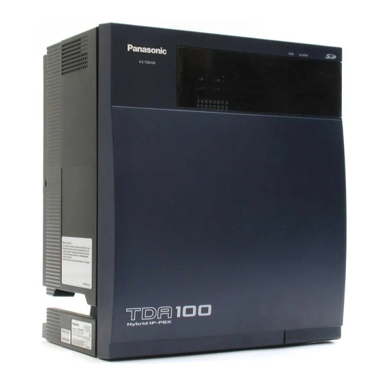
KX-TDA100CE
(for Europe)
© 2003 Panasonic Communications Co., Ltd. All
rights
reserved.
distribution is a violation of law.
ORDER NO. KMS0304728C2
Hybrid IP-PBX
Unauthorized
copying
and
Advertisement
Table of Contents

Related Manuals for Panasonic TDA 100


Summary of Contents for Panasonic TDA 100
- Page 1 When this mark does appear please read and follow the special instructions described in this manual on the use of PbF and how it might be permissible to use Pb solder during service and repair work. © 2003 Panasonic Communications Co., Ltd. All rights reserved.
-
Page 2: Table Of Contents
KX-TDA100CE CONTENTS Page Page 1 ABOUT LEAD FREE SOLDER (PbF: Pb free) 11 TROUBLESHOOTING GUIDE 1.1. SUGGESTED PbF SOLDER 11.1. MPR CARD 1.2. HOW TO RECOGNIZE THAT Pb FREE SOLDER IS 12 DIAGNOSIS USED 12.1. DIAGNOSIS FEATURES 2 FOR SERVICE TECHNICIANS 12.2. -
Page 3: About Lead Free Solder (Pbf: Pb Free)
KX-TDA100CE 1 ABOUT LEAD FREE SOLDER (PbF: Pb free) Note: In the information below, Pb, the symbol for lead in the periodic table of elements, will refer to standard solder or solder that contains lead. We will use PbF when discussing the lead free solder used in our manufacturing process which is made from Tin, (Sn), Silver, (Ag), and Copper, (Cu). -
Page 4: How To Recognize That Pb Free Solder Is Used
KX-TDA100CE 1.2. HOW TO RECOGNIZE THAT Pb FREE SOLDER IS USED Marked PbF (PbF is marked around here) (Component View) PSUP1317ZB RA308 C218 X202 R247 J113 R248 BATALM C217 R243 D407 LED103 CN206 R176 R239 R164 LED101 SDIN R241 R220 R209 R232 R230... -
Page 5: Caution
KX-TDA100CE 3 CAUTION 3.1. NOTE When you note the serial number, write down all of the 11 digits. The serial number may be found on the label affixed to the bottom of the unit. 3.2. SAFETY PRECAUTIONS 1. Before servicing, unplug the power cord to prevent an electric shock. 2. -
Page 6: Specifications
KX-TDA100CE 4 SPECIFICATIONS 4.1. GENERAL DESCRIPTION Control Bus Original bus (16 bit, 8 MHz,10 megabytes per second) Communication Bus H.100 bus conformity (1024 time slot) Switching Non Blocking Distributed Time Switch Power Input PSU-S 100 V AC to 130 V AC/200 V AC to 240 V AC, 1.4 A/0.8 A, 50 Hz/60 Hz (KX-TDA0108) PSU-M 100 V AC to 130 V AC/200 V AC to 240 V AC, 2.5 A/1.4 A, 50 Hz/60 Hz... -
Page 7: System Capacity
KX-TDA100CE 4.3. SYSTEM CAPACITY 4.3.1. Maximum Trunk and Extension Cards The following number of trunk and extension cards can be installed in the Hybrid IP-PBX for expansion. Card Type KX-TDA100 Trunk Card *1 Extension Card Total *1 One T1, E1, PRI30 and PRI23 card counts as 2 cards. Note: ·... -
Page 8: System Overview
KX-TDA100CE 5 SYSTEM OVERVIEW 5.1. SYSTEM CONFIGURATIONS... -
Page 9: System Components
Blank Slot Cover KX-T30865X Doorphone Available Telephones The Hybrid IP-PBX supports all of the Panasonic X-T7xxx and KX-TD7xxx series: · Digital/Analog proprietary telephones (e.g., KX-T7625, KX-T7630, KX-T7633, KX-T7636) · Portable stations (e.g., KX-TD7590) · DSS consoles (e.g., KX-T7640) · Single line telephones (e.g., KX-T7710) The Hybrid IP-PBX does not support the following telephones: ·... -
Page 10: System Connection Diagram
KX-TDA100CE · The power supply capacity of the Hybrid IP-PBX may differ from the values described in this manual depending on the model number.Please consult your dealer for detailed information. 5.3. SYSTEM CONNECTION DIAGRAM... - Page 11 KX-TDA100CE *Only 1 Server PC can be connected to the Hybrid IP-PBX.Two or more Server PCs cannot be used simultaneously.
-
Page 12: Name And Locations
KX-TDA100CE 6 NAME AND LOCATIONS · Null slot : Null slot is not available for any optional service card. · RUN Indicator : Shows the system normally working by green light. · ALARM Indicator : Shows the system detected some obstacles. ·... -
Page 13: Disassembly Instructions
KX-TDA100CE 7 DISASSEMBLY INSTRUCTIONS 7.1. DISASSEMBLY INSTRUCTION (MPR CARD) 1. Remove the Lib by sliding it in the direction of the arrow 1. 2. This will be removed if the user attaches the Pad Lock as shown in a Fig.1. 3. -
Page 14: Disassembly Instruction (Back Board)
KX-TDA100CE 7.2. DISASSEMBLY INSTRUCTION (BACK BOARD) 1. Remove four Screws (A). 2. Remove the Left Side Cover and the Right Side Cover. 3. Remove the Hook. And remove the Top Cover. 4. Remove nine Screws (B). 5. Remove the Back Cover. - Page 15 KX-TDA100CE 6. Remove the RS-232C Connector and LED Connector from the Back Board 1. 7. Remove eight Screws (C). 8. Remove the Back Board 1. 9. Remove the LED Connector from the Back Board 2. 10. Remove the Screw (C). 11.
-
Page 16: Outline
KX-TDA100CE 8 OUTLINE 8.1. GENERAL DESCRIPTION The control system of this unit is composed of the main control section (MPR) controlling the entire system, exchanging voice data, the circuit control section (LPR) controlling various telephone lines and the power supply section (POWER). MPR, LPR and POWER are connected each other through the System BUS (ADDRESS BUS, DATA BUS and CONTROL BUS). -
Page 17: System Control
KX-TDA100CE 8.2. SYSTEM CONTROL 8.2.1. System Control Block Diagram... - Page 18 KX-TDA100CE 8.2.2. Voice (TDM Highway) Bus Block Diagram...
- Page 19 KX-TDA100CE 8.2.3. Voice Bus Logical Assignment In the line card, the CT_D line number, which is output in accordance with the inserted slot, and the time slot are assigned on a software base. For the detail of output slot for each card, refer to the service manual of card. 8.2.4.
-
Page 20: Back Board Signal Connection Diagram
KX-TDA100CE 8.3. BACK BOARD SIGNAL CONNECTION DIAGRAM 8.3.1. CT Bus System Connection Diagram... - Page 21 KX-TDA100CE 8.3.2. EC Bus System Connection Diagram...
- Page 22 KX-TDA100CE 8.3.3. System Control and Analog Signal Connection Diagram 8.3.4. Power Supply System Connection Diagram...
-
Page 23: Mpr Card Circuit Operation
KX-TDA100CE 9 MPR CARD CIRCUIT OPERATION 9.1. MPR CARD 9.1.1. Outline 1) Function · System Control · Circuit Switching (includes gain adjustment function) · Conference Call (3 people x 8 ~ 8 people x 3) · MOH · PAGING · Clock 2) Configuration ·... - Page 24 KX-TDA100CE 9.1.2. Description of Each Part LED light (BATALM): Turns on to indicate the dropping of the lithium battery voltage (less than 2.8V). LED light (SD ACCES): Turns on when the SD card is accessing. SD card slot: Mounts the system program SD card. Reset Switch: Press at the system reset.
- Page 25 IC301, IC302 IC305, IC306 IC303 +15V +3.3V +1.8V SD Card Interface MEC Card SD Card (MN5773) FLASH (Expansion Memory) SRAM SDRAM IC403 IC205 (Future option) Total:1MB Total:512KB Total:16 MB Series Reg. 4Mbit*2 4Mbit IC413 IC402 64Mbit*2 USB Interface (16bit bus) (16bit bus) (32bit bus) SW Reg.
- Page 26 KX-TDA100CE 9.1.4. Circuit Description 9.1.4.1. Outline of Block Description · CPU block This block operates the main unit control. Besides this operates various controls, select signal generation, DMA control and serial port control. This contains the built-in clock function. · ASIC block This provides the communication function between each option card, call control (TSW function), conference call, tone generation and gain control function.
- Page 27 KX-TDA100CE Signal Name Function nBACK Bus Acknowledge: This indicates Bus Acknowledge. nBATT This indicates whether external battery is connected or not.L: Connected nBAT_ALM Battery Alarm Signal: This indicates the declined voltage of lithium battery. (L: Alarm condition) nBREQ Bus Request: Bus request signal Bus Cycle Start: Bus cycle start signal nCASL Lower Byte Address Column Address Strobe: CAS signal for SDRAM...
- Page 28 KX-TDA100CE Signal Name Function nIRQ_ASIC Interrupt Request from ASIC: This indicates ASIC requests interrupt. nIRQ_SDB Interrupt Request from SD card I/F: This indicates SD card I/F requests interrupt. nIRQ_USB Interrupt Request from USB I/F: This indicates USB I/F requests interrupt. LA[1] -[16] Address bus Lower Byte Select: This indicates Lower byte select signal of SRAM...
- Page 29 KX-TDA100CE · ASIC block Configuration: IC102 (ASIC), IC111, X103 and so on. Function: (IC102) This Functions as the bus master of EC bus (synchronous bus with 16 bit width, transmission rate max.10Mbps). Communicates with ASIC mounted to each option card via EC bus and controls the option card. Controls CT bus (HW clock 8.192MHz, 8 highway, 128 timeslot) for TSW function.
- Page 30 KX-TDA100CE in IC413, C453 and C454. +3.3V generated in DC/DC converter is converted to 1.8V in the back board or IC403 and Q405 via Q404 and supplied to IC101 core power, and also is converted to 1.9V in IC404 via the back-flow prevention diode D407 and supplied to IC101 clock block power.
-
Page 31: Back Board Circuit Operation
KX-TDA100CE 10 BACK BOARD CIRCUIT OPERATION The back board (BB) connects signals between all cards in KX-TDA100. It also supplies power from the power supply unit to the cards. CONNECTORS EXPLANATION (1) Power Supply Unit Connector: CN100 (2) Free Slot Connectors: CN102-CN106 (3) Option Card Slot Connector: CN107 (4) MPR Card Connector: CN112 (5) RS-232C Connector: CN113... -
Page 32: Troubleshooting Guide
KX-TDA100CE 11 TROUBLESHOOTING GUIDE 11.1. MPR CARD 11.1.1. Startup... - Page 33 KX-TDA100CE...
- Page 34 KX-TDA100CE...
- Page 35 KX-TDA100CE...
- Page 36 KX-TDA100CE...
- Page 37 KX-TDA100CE 11.1.2. Phone Call...
- Page 38 KX-TDA100CE 11.1.3. Paging...
- Page 39 KX-TDA100CE...
- Page 40 KX-TDA100CE...
- Page 41 KX-TDA100CE 11.1.4. MOH Using...
- Page 42 KX-TDA100CE...
- Page 43 KX-TDA100CE...
- Page 44 KX-TDA100CE 11.1.5. USB Connection...
- Page 45 KX-TDA100CE...
- Page 46 KX-TDA100CE 11.1.6. RS-232C Connection...
- Page 47 KX-TDA100CE...
- Page 48 KX-TDA100CE 11.1.7. SD Card I/F...
- Page 49 KX-TDA100CE 11.1.8. Other...
-
Page 50: Diagnosis
KX-TDA100CE 12 DIAGNOSIS 12.1. DIAGNOSIS FEATURES Card Test and Pair Port Test is in Diagnosis Features. 12.1.1. Card Test Card Test -SUMMARY Description Diagnose all kind of Cards. Parallel of Diagnose item of Card Tests and every Cards DHLC SLC8/L MSLC/ CS-INF LCOT OPB3... - Page 51 KX-TDA100CE 12.1.1.2. Card CT Bus Diagnosis Diagnose CT bus by Loop back test to use CT bus DHLC SLC8/L MSLC/ CS-INF LCOT OPB3 E&M CTI- SLC8 SLC16 LINK Object of Card Diagnosis result Card CT bus diagnosis OK Card CT bus diagnosis NG 12.1.1.3.
- Page 52 KX-TDA100CE 12.1.1.6. DSP DTMF Receiver Diagnosis Diagnose DTMF receiver of DSP in the Card to use DTMF generator of DSP DHLC SLC8/L MSLC/ CS-INF LCOT OPB3 E&M CTI- SLC8 SLC16 LINK Object of Card Diagnosis point Time slot Time slot test Primary circuit Primary circuit loop back test DSP ST loop back...
- Page 53 KX-TDA100CE 12.1.1.10. Super Frame Synchronization Diagnosis Diagnose Super frame synchronization feature of CS-INF DHLC SLC8/L MSLC/ CS-INF LCOT OPB3 E&M CTI- SLC8 SLC16 LINK Object of Card Diagnosis point DECT DECT super frame synchronization test SS super frame synchronization test Diagnosis result Super frame synchronization diagnosis OK Super frame synchronization diagnosis NG...
-
Page 54: Diagnosis Test
KX-TDA100CE 12.2. DIAGNOSIS TEST 1. Click [Diagnosis] of [Utility]. - Page 55 KX-TDA100CE 2. Pair Port Test operation Select card for Test. 3. Click [Pair Port Test].
- Page 56 KX-TDA100CE 4. Click [OK]. 5. Click [Cancel].
- Page 57 KX-TDA100CE 6. Card Test operation Select card for Test. 7. Click [Card Test].
- Page 58 KX-TDA100CE 8. Click [OK]. 9. Click [Cancel].
-
Page 59: Ic Data
KX-TDA100CE 13 IC DATA 13.1. IC101 Pin No. Pin Name Description Clock mode setting Clock mode setting Vcc-TRC*1 Power for RTC XTAL2 Crystal oscillator terminal for built-in RTC EXTAL2 Crystal oscillator terminal for built-in RTC (*6) Vcc-TRC*1 Power for RTC Nonmaskable interrupt request IRQ0/IRL0/PTH[0] External interrupt request/input port H... - Page 60 KX-TDA100CE Pin No. Pin Name Description Power supply (*3) Power supply (*3) D18/PTA[2] Data bus/I/O port A D17/PTA[1] Data bus/I/O port A D16/PTA[0] Data bus/I/O port A VssQ Power for I/O (0V) Data bus VccQ Power for I/O (3.3V) Data bus Data bus Data bus Data bus...
- Page 61 KX-TDA100CE Pin No. Pin Name Description WE3/DQMUU/ICIOW O/I/O D31-D24 select signal/DOM (SDRAM) /PCMCIA I/O write/I/O port K R/PTK[7] RD/WR Read/Write AUDSYNC/PTE[7] O/I/O AUD synchronization/I/O port E VssQ Power for I/O (0V) CS0/MCS[0] Chip select 0/mask ROM chip select 0 VccQ Power for I/O (3.3V) CS2/PTK[0] O/I/O...
- Page 62 KX-TDA100CE Pin No. Pin Name Description Power supply (*3) XTAL Clock oscillator terminal EXTAL External clock/crystal oscillator terminal STATUS0/PTJ[6] O/I/O Processor status STATUS0/PTJ[7] O/I/O Processor status TCLK/PTH[7] Clock I/O for TMU or RTC/I/O port J IRQOUT Interrupt request notification VssQ Power for I/O (0V) CKIO System clock I/O...
-
Page 63: Terminal Guide Of Ics, Transistors And Diodes
KX-TDA100CE 14 TERMINAL GUIDE OF ICS, TRANSISTORS AND DIODES... -
Page 64: How To Replace A Flat Package Ic
KX-TDA100CE 15 HOW TO REPLACE A FLAT PACKAGE IC 15.1. PREPARATION 15.3. REMOVING SOLDER FROM BETWEEN PINS · PbF (: Pb free) Solder · Soldering Iron 1. Add a small amount of solder to the bridged pins. Tip Temperature of 700°F ± 20°F (370°C ± 10°C) 2. -
Page 65: Cabinet And Electrical Parts Location
KX-TDA100CE 16 CABINET AND ELECTRICAL PARTS LOCATION... -
Page 66: Extension Boards For Servicing
KX-TDA100CE 16.1. EXTENSION BOARDS FOR SERVICING... -
Page 67: Accessories And Packing Materials
KX-TDA100CE 17 ACCESSORIES AND PACKING MATERIALS... -
Page 68: Replacement Parts List
KX-TDA100CE 18 REPLACEMENT PARTS LIST Note: Ref. Part No. Part Name & Description Remarks 1. RTL (Retention Time Limited) PSMH1205Z CHASSIS, LED The marking (RTL) indicates that the Retention Time is PSHD1091Z BOLT WITH NUT limited for this item. PSKV1016Z1 COVER, RIGHT SIDE ABS-HB After the discontinuation of this assembly in production, the... -
Page 69: Mpr Card Parts
KX-TDA100CE Ref. Part No. Part Name & Description Remarks 18.3. MPR CARD PARTS D409 MA728 DIODE(SI) Ref. Part No. Part Name & Description Remarks DA401 MA143 DIODE(SI) PCB1 PSWP1DA100CE MPR CARD ASS´Y (RTL) DA402 MA143 DIODE(SI) (ICS) LED101 PSVD1VGCT IC101 C2DBYJ000009 LED103 PSVD1SRCT... - Page 70 KX-TDA100CE Ref. Part No. Part Name & Description Remarks Ref. Part No. Part Name & Description Remarks RA306 D1HA1038A005 RESISTOR ARRAY C174 ECUV1C104ZFV RA307 D1HA1038A005 RESISTOR ARRAY RA308 D1HA1038A005 RESISTOR ARRAY C201 ECUV1H220JCV RA309 D1HA1038A005 RESISTOR ARRAY C202 PQCUV1A225ZF C203 ECUV1H220JCV (CAPACITORS) C204...
- Page 71 KX-TDA100CE Ref. Part No. Part Name & Description Remarks Ref. Part No. Part Name & Description Remarks R137 ERJ3GEYJ103 C430 ECUV1H153KBV 0.015 R138 ERJ3GEYJ103 C431 ECUV1H153KBV 0.015 R139 ERJ3GEYJ103 C433 ECUV1C104ZFV C435 ECUV1A105ZFV R140 ERJ3GEYJ330 C436 ECUV1A105ZFV R142 ERJ3GEYJ330 C437 ECUV1H333KBV 0.033 R143...
- Page 72 KX-TDA100CE Ref. Part No. Part Name & Description Remarks Ref. Part No. Part Name & Description Remarks R241 ERJ3GEYJ473 R455 ERJ3GEYJ223 R242 ERJ3GEYJ473 R456 ERJ3GEYJ223 R243 ERJ3GEYJ104 100k R457 ERJ3GEYJ223 R244 ERJ3GEYJ472 4.7k R458 ERJ3GEYJ472 4.7k R245 ERJ3GEYJ473 R459 ERJ3GEYJ472 4.7k R246 ERJ3GEYJ473...
- Page 73 KX-TDA100CE Ref. Part No. Part Name & Description Remarks Ref. Part No. Part Name & Description Remarks J115 PQ4R18XJ000 L115 ERJ3GEY0R00 J116 PQ4R18XJ000 L116 ERJ3GEY0R00 J121 ERJ3GEY0R00 L117 ERJ3GEY0R00 J123 ERJ3GEY0R00 L118 ERJ3GEY0R00 J126 ERJ3GEY0R00 L119 ERJ3GEY0R00 J129 ERJ3GEY0R00 J130 ERJ3GEY0R00 L120 ERJ3GEY0R00...
-
Page 74: Back/Led Board Parts
KX-TDA100CE Ref. Part No. Part Name & Description Remarks Ref. Part No. Part Name & Description Remarks L186 PFVF1A471SG CERAMIC FILTER X101 PSVCC0025GT CRYSTAL OSCILLATOR L187 PFVF1A471SG CERAMIC FILTER X102 PSVCC0019CT CRYSTAL OSCILLATOR L189 PFVF1B470SB CERAMIC FILTER X103 H1B1635B0016 CRYSTAL OSCILLATOR X201 H0J120500019 CRYSTAL OSCILLATOR... -
Page 75: Fixtures And Tools
KX-TDA100CE Ref. Part No. Part Name & Description Remarks R151 ERJ3GEYJ103 R152 ERJ3GEYJ103 R153 ERJ3GEYJ103 R154 ERJ3GEYJ103 R155 ERJ3GEYJ103 R156 ERJ3GEYJ103 R157 ERJ3GEYJ103 R165 ERJ3GEYJ103 R166 ERJ3GEYJ103 R167 ERJ3GEYJ103 R168 ERJ3GEYJ103 R169 ERJ3GEYJ103 R170 ERJ3GEYJ103 R177 ERJ3GEYJ103 R178 ERJ3GEYJ103 R179 ERJ3GEYJ103 R180 ERJ3GEYJ103... -
Page 76: For The Schematic Diagram
KX-TDA100CE 19 FOR THE SCHEMATIC DIAGRAM Note: 1. DC voltage measurements are taken with an oscilloscope or a tester with a ground. 2. The schematic diagrams and circuit board may be modified at any time with the development of new technology. -
Page 77: Schematic Diagram
20 SCHEMATIC DIAGRAM 20.1. MPR CARD L194 C101 2.2u C102 1.0u C103 0.1u J121 J122 C104 0.1u C106 0.1u 0.1u C107 0.1u 16.384MHz C108 0.1u C105 J123 J124 X101 C110 0.1u 0.1u 0.1u C111 C112 0.1u C161 3.3V C171 C172 C118 C117 R552... - Page 78 R198 4.7K R139 TP335 R561 R560 IC125 IC125 C_CS[0] R566 0.1u DCLK_RMT TP2039 DOUT_RMT TP2040 C162 IC131 DIN_RMT R526 R569 0.1u C174 0.1u J130 C465 J126 J129 PLLCLK 0.1u J127 R562 C141 0.1u C139 1.0u C142 0.1u 0.1u R143 C140 C144 0.1u C163...
- Page 79 A[0-25] A[0-25] A[0-25] A[0-25] D[0-31] CN210 J201 IC203 TP663 L203 TP643 R228 LD[0-15] DO1+ FIL203 TP664 TP651 TP678 TP635 SHW_CLK LA[1-16] TP665 L204 R229 TP644 TP652 DO1- +3.3V +3.3V TP666 J202 TP636 3.3V IC205 TP667 IC206 LA[1] LD[0] MNA1 MND0 J203 LA[2] LD[1]...
- Page 80 A[0-25] D[0-31] LD[0-15] LA[1-16] A[19] J301 +3.3V +3.3V +3.3V_CPU A[22] J307 RA308 RA301 RA305 TP703 J302 A[20] A[23] J308 TP712 LD[15] D[31] A[25] LD[14] D[30] A[24] J303 IC309 J309 LD[13] D[29] A[23] IC310 LD[12] TP704 TP706 J329 D[28] A[22] A[21] J304 A[24] J310...
- Page 81 +3.3V +3.3V +3.3V C422 0.1u TP816 TP826 LDHW[0] VagRef TP817 TP891 LUHW[0] R423 /PDI TP832 TP818 LHWCLK[0] MCKL BCLKR J402 TP865 1.0u TP873 L405 TP836 BCLKT JK402 C469 TP833 R429 C442 TP899 L414 1000p FIL403 C470 L415 TP819 CH_SEL[0] 1000p 1.0u L406 TP866...
-
Page 82: Back/Led Board
20.2. BACK/LED BOARD +40V +15V +40V +40V +40V +15V +15V +15V +15VPT +15VPT +15VPT +15VPT +15VPT +15VPT +15VPT +15VPT +3.3V +3.3V CN102 CN103 CN104 CN101 R101 R103 R147 R149 CT_D[0] EC_nSTOP POWERGND POWERGND POWERGND POWERGND POWERGND POWERGND POWERGND POWERGND EC_CLK EC_nSTOP EC_CLK EC_nSTOP... - Page 83 +40V +15V +40V +15V +40V +15V +15VPT CN105 +15VPT +15VPT CN106 +15VPT +15VPT CN107 +15VPT POWERGND POWERGND POWERGND POWERGND POWERGND POWERGND EC_CLK EC_nSTOP EC_CLK EC_nSTOP EC_CLK EC_nSTOP EC_nTRDY EC_nPERR EC_nTRDY EC_nPERR EC_nTRDY EC_nPERR EC_nFRAME EC_PAR EC_nFRAME EC_PAR EC_nFRAME EC_PAR EC_nCBE[0] EC_nCBE[1] EC_nCBE[0] EC_nCBE[1]...
- Page 84 +40V +15V +15VPT +15VPT +3.3V +3.3V CN112 R301 R304 Reserve-A31 R323 R326 CT_D[0] POWERGND POWERGND EC_CLK EC_nSTOP R302 R305 Reserve-B31 CN113 R324 R327 CT_D[1] EC_nTRDY EC_nPERR L104 EC_nFRAME EC_PAR L105 R303 R306 Reserve-A32 R325 R328 EC_nCBE[0] EC_nCBE[1] CT_D[2] L106 EC_AD[11] EC_nRST L107 R307...
-
Page 85: Waveform
20.3. WAVEFORM Waveform 1 Waveform 2 Waveform 3 16.384MHz 32.768kHz 65.536MHz Waveform 4 Waveform 5 Waveform 6 16.384MHz Switching the frequency of 20Hz/25Hz is Switching the pulse spacing of 2976msec/3840msec possible by the soft setting. /4992msec/5120msec is possible by the soft setting. The abobe-mentioned waveform is the The abobe-mentioned waveform is the example of example of 20Hz. - Page 86 Waveform 8 Waveform 7 20MHz 12MHz...
-
Page 87: Printed Circuit Board
21 PRINTED CIRCUIT BOARD 21.1. MPR CARD C408 CN103 C402 IC413 L401 R504 J301 R192 IP401 J329 R194 L161 L165 L167 IC309 J330 RA136 IC310 IC127 IC201 J331 R193 RA134 L164 R196 IC311 RA137 J304 R563 L166 R519 J305 J160 L163 R195 L173 J134... - Page 88 C404 L413 Q412 RA129 RA128 RA127 RA126 RA125 RA124 RA123 RA133 Q403 Q404 3.3V BB R403 C416 R406 IC402 L403 C420 D403 +3.3V +15VIN C321 C206 C322 C162 C320 R175 C163 C148 C175 Q101 C411 J136 C410 C150 R172 J316 J315 D406 R161...
-
Page 89: Back/Led Board
21.2. BACK/LED BOARD LED202 LED201 KX-TDA100 BACK/LED BOARD COMPONENT VIEW... - Page 90 +15VPT +15VPT LED202 +15V +40V +15VPT Power GND Power GND EC_nSTOP EC_CLK +15V EC_nPERR EC_nTRDY +15V EC_PAR EC_nFRAME EC_nCBE[1] EC_nCBE[0] +40V LED201 EC_nRST EC_AD[5] EC_AD[4] EC_AD[3] EC_AD[2] EC_AD[1] EC_AD[0] EC_AD[6] EC_AD[11] EC_AD[1] EC_AD[0] Power GND EC_AD[3] EC_AD[2] EC_AD[5] EC_AD[4] EC_AD[7] EC_AD[6] EC_AD[9] EC_AD[8]...
- Page 91 KX-TDA100CE KXTDA100CE...