
Related Manuals for Asus AAEON BOXER-6710


Summary of Contents for Asus AAEON BOXER-6710
- Page 1 BOXER-6710 Fanless Embedded Box PC User ’s Manual 4 Last Updated: October 12, 2021...
- Page 2 Copyright Notice This document is copyrighted, 2021. All rights are reserved. The original manufacturer reserves the right to make improvements to the products described in this manual at any time without notice. No part of this manual may be reproduced, copied, translated, or transmitted in any form or by any means witho ut the prior written permission of the original manufacturer.
- Page 3 Acknowledgements All other products’ name or trademarks are properties of their respective owners. Microsoft Windows is a registered trademark of Microsoft Corp. ⚫ Intel®, Pentium®, and Celeron® are registered trademarks of Intel ⚫ Corporation ITE is a trademark of Integrated Technology Express, Inc. ⚫...
- Page 4 Packing List Before setting up your product, please make sure the following items have been shipped: I t em Quantity BOXER-6710 ⚫ 3 Pin DC-In Power Connector ⚫ Din Rail bracket ⚫ Screw Package ⚫ If any of these items are missing or damaged, please contact your distributor or sales representative immediately.
- Page 5 About this Document This User’s Manual contains all the essential information, such as detailed descriptions and explanations on the product’s hardware and software features (if any), its specifications, dimensions, jumper/connector settings/definitions, and driver installation instructions (if any), to facilitate users in setting up their product. Users may refer to the product page at AAEON.com for the latest version of this document.
- Page 6 Saf e ty Precautions Please read the following safety instructions carefully. It is advised that you keep this manual for future references All cautions and warnings on the device should be noted. All cables and adapters supplied by AAEON are certified and in accordance with the material safety laws and regulations of the country of sale.
- Page 7 As most electronic components are sensitive to static electrical charge, be sure to ground yourself to prevent static charge when installing the internal co mponents. Use a grounding wrist strap and contain all electronic components in any static-shielded containers. If any of the following situations arises, please the contact our service personnel: Damaged power cord or plug Liquid intrusion to the device iii.
- Page 8 FCC Statement This device complies with Part 15 FCC Rules. Operation is subject to the following two conditions: (1) this device may not cause harmful interference, and (2) this device must accept any interference received including interference that may cause undesired operation.
- Page 9 Chi na RoHS Requirements ( CN) 产品中有毒有害物质或元素名称及含量 AAEON System QO4-381 Rev.A0 有毒有害物质或元素 部件名称 铅 汞 镉 六价铬 多溴联苯 多溴二苯 醚(PBDE) (Pb) (Hg) (Cd) (Cr(VI)) (PBB) 印刷电路板 × ○ ○ ○ ○ ○ 及其电子组件 外部信号 × ○ ○ ○ ○ ○ 连接器及线材...
- Page 10 Chi na RoHS Requirement (EN) Hazardous and Toxic Materials List AAEON System QO4-381 Rev.A0 Hazardous or Toxic Materials or Elements Component Name PCB and Components Wires & Connectors for Ext.Connections Chassis CPU & RAM HDD Drive LCD Module Optical Drive Touch Control Module Battery...
-
Page 11: Table Of Contents
Table of Contents Chapter 1 - Product Specifications..............1 Specifications .................... - Page 12 Chapter 3 - AMI BIOS Setup..............22 System Test and Initialization ...............
- Page 13 IRQ Mapping Chart ..................58 Appendix C – Glue Removal Procedure ............59 Removing Glue from Y our System...............
-
Page 14: Chapter 1 - Product Specifications
Chapter 1 Chapter 1 - Product Specifications... -
Page 15: Specifications
1 .1 Spe cifications System CP U Intel® Pentium® processor N4200 Intel® Celeron® processor N3350 Chip set Intel® System on Chip Sys tem Memory DDR3L 1866 MHz SODIMM slot x 1, up to 8GB Dis play Interface HDMI, VGA St orage Device HDD/SSD optional mSATA N etwork... - Page 16 Me chanical Mo unting DIN Rail Mount Dimensions (W x H x D) 44mm(W) x 166mm(H) x 106mm(D) Gross Weight 3.08 lbs. (1.4kg) N et Weight 1.32 lbs. (0.6kg) E nvironmental -20°C ~ 60°C with W.T. SSD/HDD/mSATA Op erating Temperature (according to IEC68-2-14 with 0.5 m/s airflow;...
-
Page 17: Chapter 2 - Hardware Information
Chapter 2 Chapter 2 – Hardware Information... -
Page 18: Dimensions
Di mensions 1 0 6 , 6 Chapter 2 – Hardware Information... -
Page 19: Jumpers And Connectors
2.2 Jum pers and connectors Chapter 2 – Hardware Information... -
Page 20: List Of Jumpers
2.3 Li st of Jumpers Please refer to the table below for all of the system’s jumpers that you can configure for your application Lab el F unction JP 5 AT/ATX mode select JP 10 Clear CMOS 2.3 .1 Se tting Jumpers Y ou configure your card to match the needs of your application by setting jumpers. -
Page 21: Auto Power Button (Jp5)
2.3 .2 Auto Power Button ( JP5) Disable Enable (Default) JP 5 F unction 1- 2 ATX (Default)- 2- 3 2.3 .3 Cl e ar CMOS (JP10) JP 10 F unction 1- 2 Normal (Default) 2- 3 Clear CMOS Chapter 2 – Hardware Information... -
Page 22: List Of Connectors
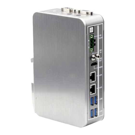
2.4 Li st of Connectors Please refer to the table below for all of the system’s connectors that you can co nfigure for your application Lab el F unction CN 65 CRT port (BOX connector) CN 38 DC-IN CN 61 HDMI connector CN 8 SPI ROM connector... - Page 23 Lab el F unction SI M1 SIM1 card connector CN 39 SATA LED connector DI MM1 SO DIMM connector Chapter 2 – Hardware Information...
-
Page 24: Mini Card Connector (Cn33, Cn5)
2.4.1 Mi ni Card Connector ( CN33, CN5) P in Sig nal P in Sig nal PCIE_WAKE# +V3.3A +1.5V PCIE_CLK_REQ# UIM_PWR UIM_DATA PCIE_REF_CLK- UIM_CLK PCIE_REF_CLK+ UIM_RST UIM_VPP W_DISABLE# PCIE_RST# PCIE_RX- +V3.3A PCIE_RX+ +1.5V SMB_CLK PCIE_TX- SMB_DATA PCIE_TX+ USB_D- USB_D+ +V3.3A +V3.3A +1.5V Chapter 2 –... -
Page 25: Lpc Port (Cn45)
P in Sig nal P in Sig nal +V3.3A 2.4.2 LPC Port ( CN45) P in P in Name Sig nal Type Sig nal Level LAD0 +3.3V LAD1 +3.3V LAD2 +3.3V LAD3 +3.3V +3.3V +3.3V LFRAME# LRESET# +3.3V LCLK I2C CLK +3.3V I2C DATA +3.3V... -
Page 26: Sata Port (Cn4)
2.4.3 SATA Port (CN4) P in P in Name Sig nal Type Sig nal Level GND # SATA_TX+ DIFF SATA_TX- DIFF SATA_RX- DIFF SATA_RX+ DIFF 2.4.4 SATA PW R Port (CN3) P in P in Name Level +12V Chapter 2 – Hardware Information... -
Page 27: Usb 3.0 (Cn26, Cn27)
2.4.5 USB 3.0 (CN26, CN27) P in Sig nal P in Sig nal VBUS_1 VBUS_2 (A)D- (B)D- (A)D+ (B)D+ (A)SSRX- (B)SSRX- (A)SSRX+ (B)SSRX+ (A)SSTX- (B)SSTX- (A)SSTX+ (B)SSTX+ Chapter 2 – Hardware Information... -
Page 28: Vga Port Box Connector (Cn65)
2.4.7 VG A port BOX connector (CN65) P in Sig nal P in Sig nal VSYNC HSYNC DDC_CLK DDC_DATA Blue Green VGA_VCC 2.4.8 DC-IN ( CN38) P in Sig nal P in Sig nal PWR_IN 2.4.9 HDMI Port (CN61) P in Sig nal P in Sig nal... -
Page 29: Spi Rom Connector For Debugging (Cn8)
P in Sig nal P in Sig nal HDMI_SCL HDMI_SDA HDMI_PWR HDMI_HDP 2.4.10 SPI ROM connector f or debugging ( CN8) P in Sig nal P in Sig nal SPI_VCC SPI_CE SPI_CLK SPI_DATA_OUT SPI_DATA_IN 2.4.11 Re m ote switch connector (CN63) P in Sig nal P in... -
Page 30: Usb2.0 Connector (Internal Box Connector) (Cn53, Cn54)
2.4.12 USB2.0 connector (internal BOX connector) (CN53, CN54) P in Sig nal P in Sig nal VBUS USB1- USB+ 2.4.13 Powe r Switch connector (internal BOX connector) (CN36) P in Sig nal P in Sig nal PANSWH# GND- 2.4.15 COM port RS-232/422/485 BOX connector ( CN18/CN9/CN12/CN14) P in R S-232 R S-422... - Page 31 P in R S-232 R S-422 R S-485 Chapter 2 – Hardware Information...
-
Page 32: Hdd & Ram Installation
2.5 HDD & RAM Installation Remove the screws as shown below; then remove the cover. Chapter 2 – Hardware Information... - Page 33 Put the thermal pad on between the chassis and the RAM, slot in the RAM diagonally into the slot and push down to secure. * 6 M3 SCREW PAD 2 0 * 1 0 * 0 . 7 * 2 M3 SCREW PAD 6 6 * 2 0 * 4 RAM HEATSINK Chapter 2 –...
-
Page 34: Din Rail Installation
2.6 Di n Rail Installation Chapter 2 – Hardware Information... -
Page 35: Chapter 3 - Ami Bios Setup
Chapter 3 Chapter 3 - AMI BIOS Setup... -
Page 36: System Test And Initialization
System Test and Initialization The system uses certain routines to perform testing and initialization. If an error, fatal or non-fatal, is encountered, a few short beeps or an error message will be outputted. The board can usually continue the boot up sequence with non-fatal errors. The system configuration verification routines check the current system configuration against the values stored in the CMOS memory. -
Page 37: Ami Bios Setup
3.2 AMI BIOS Setup The AMI BIOS ROM has a pre-installed Setup program that allows users to modify basic system configurations, which is stored in the battery-backed CMOS RAM and BIOS NVRAM so that the information is retained when the power is turned off. To enter BIOS Setup, press <Del>... -
Page 38: Setup Submenu: Main
3.3 Se tup Submenu: Main Chapter 3 – AMI BIOS Setup... -
Page 39: Setup Submenu: Advanced
3.4 Se tup Submenu: Advanced Chapter 3 – AMI BIOS Setup... -
Page 40: Advanced: Trusted Computing
3.4.1 Advanced: Trusted Computing Options summary: Security Device Disabled Optimal Default, Failsafe Default Support Enabled Enable/Disable Security Device. NOTE: Y our Computer will reboot during restart in order to change State of the Device. SHA-1 PCR Bank Disabled Enabled Optimal Default, Failsafe Default Enable or Disable SHA-1 PCR Bank SHA256 PCR Bank Disabled... - Page 41 Storage Hierarchy Disabled Enabled Optimal Default, Failsafe Default Enable or Disable Storage Hierarchy Endorsement Disabled Hierarchy Enabled Optimal Default, Failsafe Default Enable or Disable Endorsement Hierarchy TPM2.0 UEFI Spec TCG_2 Optimal Default, Failsafe Default Version TCG_1_2 Select the TCG2 Spec Version Support, TCG_1_2: the Compatible mode for Win8/Win10, TCG_2: Support new TCG2 protocol and event format for Win10 or later Physical presence...
-
Page 42: Advanced: Cpu Configuration
3.4.2 Advanced: CPU Configuration Chapter 3 – AMI BIOS Setup... - Page 43 Options summary: Active Processor Disabled Optimal Default, Failsafe Default Cores Enabled Number of cores to enable in each processor package Intel Virtualization Disabled Technology Enabled Optimal Default, Failsafe Default When enabled, a VMM can utilize the additional hardware capabilities provided by Vanderpool Technology.
- Page 44 Power Limit 1 Enable Disabled Optimal Default, Failsafe Default Enabled Enable/Disable Power Limit 1 C-States Disabled Optimal Default, Failsafe Default Enabled Enable/Disable C States Chapter 3 – AMI BIOS Setup...
-
Page 45: Advanced: Sata Drives
3.4.3 Advanced: SATA Drives Options summary: Chipset SATA Enable Optimal Default, Failsafe Default Disable Enable or Disable the Chipset SATA Controller. The Chipset SATA controller supports the 2 black internal SATA ports (up to 3Gb/s supported per port) Port Enable Optimal Default, Failsafe Default Disable Enable or Disable SATA Port... -
Page 46: Advanced: Hardware Monitor
3.4.4 Advanced: Hardware Monitor Chapter 3 – AMI BIOS Setup... -
Page 47: Advanced: Sio Configuration
3.4.5 Advanced: SIO Configuration Chapter 3 – AMI BIOS Setup... -
Page 48: Sio Configuration: Serial Port 1 Configuration
3.4.5.1 SIO Configuration: Serial Port 1 Configuration Options summary: Use This Device Disabled Enabled Optimal Default, Failsafe Default Enable or Disable this Logical Device. Possible: Use Automatic Settings Optimal Default, Failsafe Default IO=3F8; IRQ=4; IO=2F8; IRQ=3; Allows the user to change the device resource settings. New settings will be reflected on this setup page after system restarts. -
Page 49: Sio Configuration: Serial Port 2 Configuration
3.4.5.2 SIO Configuration: Serial Port 2 Configuration Options summary: Use This Device Disabled Enabled Optimal Default, Failsafe Default Enable or Disable this Logical Device. Possible: Use Automatic Settings Optimal Default, Failsafe Default IO=2F8; IRQ=3; IO=3F8; IRQ=4; Allows the user to change the device resource settings. New settings will be reflected on this setup page after system restarts. -
Page 50: Sio Configuration: Serial Port 3 Configuration
3.4.5.3 SIO Configuration: Serial Port 3 Configuration Options summary: Use This Device Disabled Enabled Optimal Default, Failsafe Default Enable or Disable this Logical Device. Possible: Use Automatic Settings Optimal Default, Failsafe Default IO=3E8; IRQ=11; IO=2E8; IRQ=11; Allows the user to change the device resource settings. New settings will be reflected on this setup page after system restarts. -
Page 51: Power Management
3.4.6 Powe r Management Options summary: Power Mode ATX Type Optimal Default, Failsafe Default AT Type Select system power mode. Restore AC Power Loss Last State Optimal Default, Failsafe Default Power On Power Loss RTC wake system from S5 Disabled Optimal Default, Failsafe Default Fixed Time Dynamic Time... -
Page 52: Setup Submenu: Chipset
3.5 Se tup submenu: Chipset Chapter 3 – AMI BIOS Setup... -
Page 53: Chipset: North Bridge
3.5.1 Chi pset: North Bridge Options summary: DCMT Total Gfx 128M 256M Optimal Default, Failsafe Default Select DVMT5.0 Total Graphics Memory size used by the Internal Graphics Device Chapter 3 – AMI BIOS Setup... -
Page 54: Chipset: South Bridge
3.5.2 Chi pset: South Bridge Options summary: HD-Audio Support Disable Enable Optimal Default, Failsafe Default Enable/Disable HD-Audio Support Mini-Card 1 Speed Auto Optimal Default, Failsafe Default Gen 1 Gen 2 Configure PCIe Speed Mini-Card 2 Speed Auto Optimal Default, Failsafe Default Gen 1 Gen 2 Configure PCIe Speed... -
Page 55: Setup Submenu: Security
3.6 Se tup submenu: Security Change User/Administrator Password Y ou can set a User Password once an Administrator Password is set. The password will be required during boot up, or when the user enters the Setup utility. Please Note that a User Password does not provide access to many of the features in the Setup utility. -
Page 56: Setup Submenu: Boot
3.7 Se tup submenu: Boot Options summary: Quiet Boot Disabled Enabled Optimal Default, Failsafe Default Enable or Disable Quiet Boot option Network Stack Disabled Optimal Default, Failsafe Default Enabled Enable/Disable UEFI Network Stack Chapter 3 – AMI BIOS Setup... -
Page 57: Setup Submenu: Save & Exit
3.8 Se tup submenu: Save & Exit Chapter 3 – AMI BIOS Setup... -
Page 58: Chapter 4 - Drivers Installation
Chapter 4 Chapter 4 – Drivers Installation... -
Page 59: Driver Download And Installatio N
Dri ver Download and Installation Drivers for the BOXER-6710 can be downloaded from the product page on the AAEON website by following this link: https://www.aaeon.com/en/p/fanless-embedded-box-pc-boxer-6710 Download the driver(s) you need and follow the steps below to install them . St ep 1 – Install Chipset Drivers Open the STEP1-Chipset folder and select your OS Open the Set upChipset.exe file in the folder Follow the instructions... - Page 60 St ep 4 – Install LAN Drivers Open the STEP4–LAN folder and select your OS Open the t ar.gz or .exe file Follow the instructions Drivers will be installed automatically St ep 5 – Install Audio Drivers Open the STEP5–Audio folder and select your OS Open the .
-
Page 61: Appendix A - Watchdog Timer Programming
Appendix A Appendix A - Watchdog Timer Programming... -
Page 62: Watchdog Timer Initial Program
Watchdog T imer Initial Program Tab le 1 : SuperIO relative register table Default Value N o te SIO MB PnP Mode Index Register I nd ex 0x2E(Note1) 0x2E or 0x4E SIO MB PnP Mode Data Register Dat a 0x2F(Note2) 0x2F or 0x4F Tab le 2 : Watchdog relative register table R egister... -
Page 63: Watchdog Sample Program
A.2 Watchdog Sample Program ************************************************************************************ // SuperIO relative definition (Please reference to Table 1) #d efine byte SIOIndex //This parameter is represented from N o te1 #d efine byte SIOData //This parameter is represented from N o te2 #d efine vo id IOWriteByte(b yte IOPort, b yte Value); #d efine b yte IOReadByte(b yte IOPort);... - Page 64 ************************************************************************************ VOID Main(){ // Procedure : AaeonWDTConfig // (byte)Timer : Time of WDT timer.(0x00~0xFF) // (boolean)Unit : Select time unit(0: second, 1: minute). AaeonWDTConfig(); // Procedure : AaeonWDTEnable // This procudure will enable the WDT counting. AaeonWDTEnable(); ************************************************************************************ Appendix A – Watchdog Timer Programming...
- Page 65 ************************************************************************************ // Procedure : AaeonWDTEnable VOID A aeonWDTEnable (){ WDTEnableDisable(Enab leLDN, EnableReg, EnableBit, 1); // Procedure : AaeonWDTConfig VOID A aeonWDTConfig (){ // Disable WDT counting WDTEnableDisable(Enab leLDN, EnableReg, EnableBit, 0); // Clear Watchdog Timeout Status WDTClearTimeoutStatus(); // WDT relative parameter setting WDTParameterSetting();...
- Page 66 ************************************************************************************ VOID SI OEnterMBPnPMode(){ IOWriteByte(SIOIndex, 0x87); IOWriteByte(SIOIndex, 0x87); VOID SI OExitMBPnPMode(){ IOWriteByte(SIOIndex, 0xAA); VOID SI OSelectLDN(byte LDN){ IOWriteByte(SIOIndex, 0x07); // SIO LDN Register Offset = 0x07 IOWriteByte(SIOData, LDN); VOID SI OBitSet(byte LDN, byte Register, byte BitNum, byte Value){ Byte TmpValue; SIOEnterMBPnPMode();...
-
Page 67: Appendix B - I/O Information
Appendix B Appendix B - I/O Information... -
Page 68: I/O Address Map
I/O Address Map Appendix B – I/O Informati o n... - Page 69 Appendix B – I/O Informati o n...
-
Page 70: Memory Address Map
B.2 Me m or y Address Map Appendix B – I/O Informati o n... - Page 71 B.3 IRQ Mapping Chart Appendix B – I/O Informati o n...
- Page 72 Appendix C Appendix C – Glue Removal Procedure...
- Page 73 Re m oving Glue f rom Your System To protect components from damage and ensure proper operation out of the box, glue may have been applied to some cables or connectors to keep them in place during shipping. This glue must be removed before attempting to swap components or perform maintenance.
- Page 74 St ep 1: Using an eyedropper or bottle as shown above, apply a few drops of alcohol to the glue. St ep 2: Allow the alcohol to soak for 10 seconds, then use a cotton swab or cotton with anti-static tweezers to evenly rub the alcohol over the glue. St ep 3: Let soak for 10 more seconds, then use anti-static tweezers to remove the glue.
- Page 75 If you encounter any issues or need support, please contact your AAEON representative or visit our Support Page at AAEON.com Appendix C – Glue Removal Procedure...