Advertisement
Quick Links
CAUTION
EXTREME CAUTION MUST BE TAKEN WHEN SERVICING THIS MACHINE. EVEN THOUGH
THE MODE SWITCH IS IN THE OFF POSITION, VOLTAGE IS STILL SUPPLIED TO THE
ENTIRE MACHINE.
WHEN WORKING ON THIS MACHINE MAKE SURE THAT THE POWER CORD IS
REMOVED FROM THE WALL OUTLET.
CHAPTER 1. SPECIFICATIONS. . . . . . . . . . . . . . . . . . . . . . . . . . . . . . . . . . . 1-1
CHAPTER 2. OPTIONS . . . . . . . . . . . . . . . . . . . . . . . . . . . . . . . . . . . . . . . . . 2-1
CHAPTER 3. SERVICE (SRV) MODE . . . . . . . . . . . . . . . . . . . . . . . . . . . . . . 3-1
CHAPTER 4. HARDWARE DESCRIPTION . . . . . . . . . . . . . . . . . . . . . . . . . . 4-1
CHAPTER 5. TEST FUNCTION . . . . . . . . . . . . . . . . . . . . . . . . . . . . . . . . . . . 5-1
CHAPTER 6. DOWN LOAD FUNCTION. . . . . . . . . . . . . . . . . . . . . . . . . . . . . 6-1
CHAPTER 7. SERVICE PRECAUTION . . . . . . . . . . . . . . . . . . . . . . . . . . . . . 7-1
CHAPTER 8. CIRCUIT DIAGRAM & PWB LAYOUT . . . . . . . . . . . . . . . . . . . 8-1
Parts marked with " ! " is important for maintaining the safety of the set. Be sure to replace these parts with specified ones
for maintaining the safety and performance of the set.
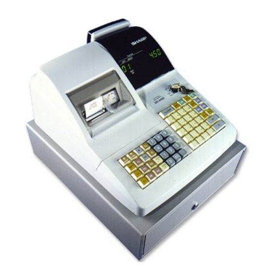
SERVICE MANUAL
ELECTRONIC
CASH REGISTER
MODEL
CONTENTS
SHARP CORPORATION
ER-A450
SRV Key : LKGIM7113RCZZ
PRINTER
: PR-45M
("V" version)
This document has been published to be used
for after sales service only.
The contents are subject to change without notice.
Advertisement

Related Manuals for Sharp ER-A450


Summary of Contents for Sharp ER-A450
-
Page 1: Table Of Contents
SERVICE MANUAL ELECTRONIC CASH REGISTER ER-A450 MODEL SRV Key : LKGIM7113RCZZ PRINTER : PR-45M ("V" version) CAUTION EXTREME CAUTION MUST BE TAKEN WHEN SERVICING THIS MACHINE. EVEN THOUGH THE MODE SWITCH IS IN THE OFF POSITION, VOLTAGE IS STILL SUPPLIED TO THE ENTIRE MACHINE. -
Page 2: Chapter 1. Specifications
CHAPTER 1. SPECIFICATIONS 1. Appearance/Rating 1) Rating ± Power source AC 230V or local voltage 50/60Hz Power consumption Standby: 14 W Maximum: 41 W (max.) Operating temperature 0°C 40°C (32°F 104°F) Operating humidity 90% (RH) ´ ´ Physical dimensions, 355(W) 424(D) 308(H)mm ´... - Page 3 3. Mode switch Customer display (Pop-up display) Fig. 4-2 7 segment display (LED) No. of positions OP,X/Z Color of display Yellow Green Character size 14.2 (H) 8.0 (W) mm X1/Z1 PGM1 X2/Z2 Display contents PGM2 (SRV) Display Description (SRV') Position Amount Fig.
- Page 4 · Cutter: Manual 2) Paper · Paper near end sensor: Item Description · Printing area: Name Heat-quality paper ± Roll dimension 44.5 0.5 mm in width Number of thermal head heater elements 864 dots Thickness 0.06 mm to 0.08 mm (688dots) 3) Cutter ·...
-
Page 5: Chapter 2. Options
CHAPTER 2. OPTIONS 1. System configuration (NOTE1) This symbol shows NEW MODEL ER-A450 LOCAL PURCHASE ER-03RA MASTER MACHINE COMPUTER OPTION RAM COMMERCIAL ER-01/02FD ER-05DW DKiT-8669BHZZ PRODUCT 3.5 inch FDD CABLE REMOTE DRAWER 1 HOLE CASHIER SWITCH Fig. 1-1 2 – 1... - Page 6 2. Options NAME MODEL DESCRIPTION EXPANSION RAM CHIP ER-03RA 512K bytes RAM CHIP REMOTE DRAWER ER-05DW PRESETS LOADER ER-01FD/02FD FD unit ´ KEY TOP KIT ER-11KT7 1 KYE TOP UNIT ´ ER-12KT7 2 KYE TOP UNIT ´ ER-22KT7 2 KYE TOP UNIT ´...
- Page 7 [key setup procedure] CHAPTER 3. SRV. RESET AND MASTER RESET MRS-2 Key position set Free key Free key setup executed complete. 1. SRV. reset (Program Loop Reset) Disable Used to return the machine back to its operational state after a lock-up has occurred.
-
Page 8: Chapter 4. Hardware Description
CHAPTER 4. HARDWARE DESCRIPTION 1. Hard ware block diagram STANDARD OPTIONAL RAM1 RAM2 ER-03RA:512KB DRAWER 128KB 512KB STANDARD GATE ARRAY TPRC1 MPCA7 OPERATER DISPLAY 512KB 1 LINE 7SEG 10DIG CUSTOMER DISPLAY 1 LINE PRINTER 7SEG 7DIG PR-45M CKDC8 SWITCH KEY BOARD RS232 1 ports Fig. - Page 9 2. Description of main LSI’s 2-1. CPU (HD6415108-10) 1) Pin configuration AVSS P57/STOP HD6415108-10 pin configuration Fig. 2-1 4 – 2...
- Page 10 2) Block diagram P27/A23 P26/A22 Data bus Port 1 P25/A21 P24/A20 P23/A19 P22/A18 P21/A17 P20/A16 EXTAL XTAL Clock Watch oscillator dog timer H8/500 CPU STBY Interruption controller 16bit free running Refresh controller timer x 2ch RFSH BREQ BACK Wait state 8bit timer controller WAIT...
- Page 11 3) Pin description SIGNAL SIGNAL SYMBOL FUNCTION SYMBOL FUNCTION NAME NAME /RES /RESET RESET INPUT from CKDC WUTH /PRST Printer (PR-45) Reset signal from BUFFER MPCA NON-MASKABLE INTERRUPT INPUT /NEJ Near END signal jounal FOR SSP INTERRUPT INPUT (NU) GND /NER Near END signal receipt EVENT READ CANCEL (to CKDC)
- Page 12 2-2. G.A (MPCA7) 1) Pin configuration EXINT0 EXINT1 PCUT EXINT2 FCUT EXINT3 STAMP RA15 SLRS RA16 SLMTD RA17 RA18 EXWAIT POFF WAIT INT1 HTS1 MCR1 SCK1 STH1 DAX1 RCKX IRRX UATX VRESC UARX SLTMG UASCK SLRST IRTX PHAI SDT7 SDT6 MA15 SDT5 TEST...
- Page 13 2) Block diagram A23~A0 IRLON ROS1 ROS2 Address decode RASEL RAS1 SSPRQ SSP comparison register External CS Image BAR. RAS2 Internal CS control RAS3 OPTCS IRTX IRRX I/R Control D0~D7 ASKRX Buffer TXDI SCKI RXDI HTS1 Multiplexer SCK1 serial select STH1 HTS2 SCK2...
- Page 14 3) Pin description Signal Signal Function Function name name Receipt side paper feed solenoid (NU) 8 bit serial port output to CPU RXD2 Journal side paper feed solenoid (NU) 8 bit serial port input from CPU TXD2 Printer partial cut signal (NU) Serial port shift clock input from CPU.
- Page 15 2-3. CKDC8 Signal Function name 1) Pin configulation — MCR1 — MCR2 Wait request signal WAIT External wait control input signal (NU) EXWAIT RA18 RA17 /RESETS — /SHEN RA16 LDRQ RA15 Expansion RD signal CKDC8 Option Expansion WR signal RS232C /CD interrupt EXINT3 KR10 Option PWB (PULL UP)
- Page 16 2-4. TPRC1 (F258024PC) SIGNAL SYMBOL FUNCTION NAME 1) General KEY RETURN 7 TPRC1 is the LSI circuit of the peripheral circuits of the microcomputer AVRF required for thermal printer control. AVDD /RESET /RES0 Auto cutter Pulse motor 32.768 KHz POF,RES 4.19 MHz Thermal VSS1...
- Page 17 2) Pin configuration PTJM PTRM BA13 BA14 BA15 LATCH CLOCK INHDEC CSEN TEST2 TEST1 CTAO CTBO VHCOM JVPON RVPON PCRES PHUP EBACK INTI EBREQ Fig. 2-7 4 – 10...
- Page 18 3) Block diagram INHBEC CSEN DECODEK UNIT RD,WR SYSTEM POF,INH A0~23 PDCTLU D0~7 HEAD CONTROL TIMER UNIT POP,PHUP,PFP,PCRES PORT PTRM,PTJM MOTOR CONTROL CLOCK,SO,ST1~5,HCO TIMER UNIT HEAD EBAK,EPEQ MISC. CUTTER CONTROL EBRK,EACK TIMER UNIT RVPON,JVPON, MOTOR RAS,RBS,RCS,RDS, CONTROL JAS,JBD,JCS,JDS INTI TEST TEST1,TEST2 CIRCUIT CLOCK...
- Page 19 Signal Signal In/Out Function In/Out Function name name Data bus 5: Internal register, print buffer EBACK Bus acknolege to option data IO Receipt paper empty Data bus 6: Internal register, print buffer Journal paper empty data IO PHUP Printer head up Data bus 7: Internal register, print buffer PCRES Auto cutter unit reset signal input (Nu)
- Page 20 2) CKDC8 oscillation circuit Signal In/Out Function name 127 BA9 Address bus 9 for PB-RAM 128 BA8 Address bus 8 for PB-RAM 4.19MHz 129 BA7 Address bus 7 for PB-RAM 130 GND — 131 GND — 132 GND — 133 BA6 Address bus 6 for PB-RAM CKDC 8 134 BA5...
- Page 21 The voltage at the (–) pin of the comparator IC7A is always maintained 0 page memory map to 5.1V by means of the zener diode ZD2, while +24V supply voltage 000000H is divided through the resistors R114, R115 and R116, and is applied to the (+) pin.
- Page 22 RAM area memory map 2) Block diagram 100000H Data bus ROS1 ROM1 NOT USE MPCA6 1C0000H RAS1 (Not use) RAM2 1E0000H Address bus RAM1 (OPTION) RAS2 128K Byte RAS2 RAS3 200000H RAS3 512K Byte Fig. 5-6 (OPTION) ROM control 280000H C80000H~CFFFFFH ROS2 (MAX 2MB)
- Page 23 As the address detection system, the brake address register compari- 6. SSP circuit son system is employed though the mapping system was employed in the conventional monitor RAM. The address registerlocated in MPCA 1) Block diagram is always compared with the system address bus to monitor and gen- erate NMI signal at a synchronized timing and togo to NMI exception This is the circuit employed to do the Special Service Preset(SSP).
- Page 24 3) SSP register access method Access to SSP break address register is performed through the tem- porary register as shown below: A19 A18 A17 A16 A15 A8 A7 Temporary Temporary Fig. 6-5 Enable flags can be accessed individually. Information on which brake register the SSP brake is detected in is Though enable register 4 can be accessed individually, writing to read as binary data by reading address FFFFFFH (*1).
- Page 25 Receipt feed motor: The motor rotates counterclockwise. 9. Key, display, time buzzer controls Phase Step No. MPCA7 HTS1 STH1 SCK1 RESET RESET RES1 INT2 Journal feed motor: The motor rotates clockwise. POFF Phase Step No. LDRQ LDRQ SHEN SHEN P-OFF POFF Note 1: ON = Conducting OFF = Not conducting...
- Page 26 2) Power off sequence 4) DISPLAY CONTROL When the CPU senses a service interruption, it performs necessary procedures for CPU stop. Then the CPU outputs a reset request to the LED-display CKDC8. (for operator) G1-G10 Reset request SA-SG,DP LED-display (for custmer) SHEN DON'T CARE CKDC5...
-
Page 27: Chapter 5. Test Function
1) Key operation 1) This diagnostic program has been developed for diagnosing ma- chine functions in the field. The program is contained within the ER-A450. The diagnostic program is stored in the external ROM which will be 2) Functional description... - Page 28 70 15 05 16 04 13 03 12 02 11 01 00 26 25 06 3) Check items <ER-A450 STANDARD KEY BOARD LAYOUT> 1. Check that the slanted lines of special characters are clearly printed. 68 67 58 77 78 2.
- Page 29 3) Check items [STANDARD KEYBOARD LAYOUT] × × × × × × × × a) Check of the display in the test and the content of end print. SUMCHECK DATA = A4 + 0E + 04 + 2B + 17 + = 2243 4) Test termination 44 43 3A 4D 4E...
- Page 30 [7] Calendar oscillator test [9] Drawer open sensor test (For standard test) 1) Key operation 1) Key operation 2) Functional description 2) Functional description State of the drawer open sensor is sensed and displayed. This program is used to test the calendar oscillator function. Display: 1 1 0 3) Check items...
- Page 31 2) Functional description 4) Test termination Perform the following check for the standard RAM 128 KByte SRAM. The test automatically terminates with termination message. The memory contents should not be changed before and after the Normal termination print check. ROM1 27040 ***** Perform the following processes for memory address to be checked *****...
- Page 32 2) Content 2) Functional description The following check are performed for the optional RAM. Control signal check The following process is performed for memory addresses to be OUT PUT INPUT checked. PASS1: memory data save PASS2: Data "0000H" write PASS3: Data "0000H" read and comparison, data "5555H" write PASS4: Data "5555H"...
-
Page 33: Chapter 6. Down Load Function
CHAPTER 6. DOWN LOAD 3. Location of connector pins FUNCTION ECR-ECR cable 9PIN D-SUB 9PIN D-SUB 1. General RAM data can be transmitted in the following two methods. Save the data before servicing as follows: ¬¾¾® · Cable: 9 pin D-SUB – 9 pin D-SUB Fig. - Page 34 ECR-ER-02FD cable 5. Data format 25PIN D-SUB 9PIN D-SUB A single byte image of the RAM data to be transmitted is divided into a high order 4 bits and low order 4 bits and converted into ASCII code. ER-02FD Then, the image of the memory is sent in the following format: Data (128bytes) Memory top address: 0000H FFFFH...
- Page 35 7. Operational method 8. Saving/Loading of data to/From the FD unit Configuration 1) To prepare an ECR to receive data from another ECR or the ER-02FD, the memory size of the receiving unit must the same as 1) Turn off the power switch of the ER-02FD, and set the DIP or greater than the sending unit.
-
Page 36: Chapter 7. Service Precaution
3. Caution to be taken when removing the TOP CABINET After removing the ER-A450’s TOP CABINET from the BOTTOM CABINET, put the TOP CABINET on the positions given below to prevent the cable that connects the MAIN PWB and POWER SUPPLY PWB from disconnecting. -
Page 37: Chapter 8. Circuit Diagram & Pwb Layout
CHAPTER 8. CIRCUIT DIAGRAM & PWB LAYOUT POWER SUPPLY(MAIN PWB) 1/10 +24V HEAT SINK C4153 1SR154-400 220uH FUSE 1SR154-400 T800mA/250V R112 R111 3.6KF R121 C266 +24V PTZ6.2A R120 100uF KA34063A SFPL52V 1000uF R113 330uF/16V PS CN 330uF/16V FROM PS PWB 0.1uF 220P 0.1uF/50V... - Page 38 CPU(HD6415108) 2/10 10K X8 R187 R188 R189 R190 0.1u 0.1u 0.1u 47u16V 47u16V R136 R191 R192 R135 D[0..7] R193 3-8C 5-7D R194 6-5C 7-7B 3-8C 5-7D 100P 6-8B R134 7-8C R133 3-8C 5-7D 6-5B 7-7B 100P R132 R164 4.7K R131 3-8C R165 R167...
- Page 39 GATE ARRAY(MPCA7) 3/10 IC10 R229 RASP 7-6B DOTEN PCUT TWAIT /TWAIT 6-2C /RES FCUT C170 100P STAMP C148 SLRS R228 100 0.01u SLMTD STH2 4-4C (R204) R205 R206 R207 R208 R227 SCK2 FSCK 4-4C HTS2 4-4C R226 SLMTR 1-5A /POFF INT0 SLMTS INT1...
- Page 40 (NOT USED) 4/10 R237 R238 R239 R240 IC11 CN14 KIA7812 2-5C C171 /FRES FRES C173 R232 KTA1664 R233 0.1u/50V 3-1D 0.1u/50V 3-1D 1.2K 3-1D FSCK FSCK BUSY BUSY 2-5A C172 R234 2-5A 3-3A /RDY 10u/50V 3.3K VCON R241 68 "F" FMC CN R235 3.9K...
- Page 41 MAIN MEMORY 5/10 2-1D 2-1D 2-8C A[0..18] 2-8D D[0..7] 4-7D 3-8C 3-1C 3-1C RAS1 RAS2 C183 C180 100P 100P R242 C176 0 OHM 47U/16V IC13 (IC15) ROM1 IC14 C177 0.1u A18/PGM R243 0 OHM 32P DIP 1M SRAM 1M SRAM C178 C181 C184...
- Page 42 OPTION MEMORY/CONNECTOR 6/10 +24V A[0..18] CN16 2-8C 7-8A CUTM+ CUTM+ 7-4A CN15 CUTM- CUTM- 7-4A CUTS CUTS 7-3B VJCOM VJCOM 7-1A /JPFA /JPFA 7-2C /JPFB /JPFB 7-2C IC16 /JPFD /WR0 /JPFD 7-2C 3-1B /WR0 /WR0 /JPFC /RESET /JPFC 7-2C 5-6A /RESET /RESET /JPES...
- Page 43 GATE ARRAY(TPRC1) 7/10 10KX9 (R315) R313 R310 R308 C264 C230 R316 R312 R309 R314 R311 R317 C265 0.1u 74HC00S (C231) C236 IC17 C227 R246 R247 R248 R249 R250 R251 R252 R253 R307 0 OHM 10u16V 10u16V +24V /RESET 5-6A R306 6-3B /STRB1 RESET...
- Page 44 DISPLAY DRIVER(CKDC8) 8/10 A1663 A1663 A1663 A1663 A1663 A1663 A1663 A1663 A1663 A1663 KRC106SX10 G[1..10] G10' G[1'..10'] 330K 10U/16V TO POP UP LED PWB 32.768KHZ BUZZER (R5) TO FRONT LED PWB 1SS353 1-5A /POFF BD10 4.19MHz 9-5B G7' PDS' 9-5B 9-5B C2412K 2.2K...
- Page 45 KEY I/F(MAIN PWB) 9/10 8-4B ST[0..9] KEYBOARD KEY74 CN19 CN18 ST4A KR10 D D 14 8-4B KR10 KR10 ST5A ST0A D D 16 ST1A D D 17 ST2A D D 18 ST3A 1SS353X4 D D 19 CLERK_CN ST4A D D 20 ST5A D D 21 ST6A...
- Page 46 RS232C 10/10 CN21 C251 0.1U C255 0.1U C252 IC27 0.1U RS CN C254 0.1U C253 0.1U 2-1B /RSS T1IN T1OUT 2-1B /ERS T2IN T2OUT T3IN T3OUT 2-1C T4IN T4OUT R334 2-1C R1OUT R1IN R335 2-1B /CDS R2OUT R2IN R336 2-1B R3OUT R3IN R337...
- Page 47 FRONT PWB <FRONT LED PWB> G1'..G10' G10' FND5 FND4 FND3 FND2 FND1 G10' FRONT CN(18P) A'..DP'...
- Page 48 POP-UP PWB DIG7' DIG6' DIG5' DIG4' DIG3' DIG2' DIG1' FND4 FND3 FND2 FND1 POP UP CN...
- Page 49 PS PWB CN17 CAR BT CN HEAT SINK POWER UNIT KTD998 +24V 180uH SEMKO T2.5AL/250V 22KF CORE PS156R LM2574HVN 2200uF/50V +24V 3300UF M0.033u (C2) 3300UF PS CN 6,8PIN:NC (4700UF) 22UF/50v (50V) 1.2KF TO MAIN PWB CP301...
- Page 50 THERMAL PRINTER(PR.PWB) CON2 VDD(+5V) CON1 CON6 /STB4 VHIN CON7 /STB3 /JPFD CUTM+ VRCOM /JPFC CUTM- VRCOM /JPFB CUTS /RPFA /JPFA VJCOM /RPFB VJCOM VJCOM /RPFC VJCOM /JPFA 53047-0910 /RPFD /JPFB MOLEX /JPFC 53014-0610 53014-0610 /JPFD MOLEX MOLEX /JPES CON3 A-1 VH VDD(+5V) A-2 VH /STB4...
- Page 51 MAIN PWB LAYOUT (1) SIDE A...
- Page 52 (2) SIDE B...
- Page 53 PS PWB FRONT DISPLAY PWB POP-UP DISPLAY PWB 8 – 17...
-
Page 54: Parts Guide
ER-A450V PARTS GUIDE ER-A450 MODEL PRINTER : PR-45M SRV key : LKGIM7113BHZZ (for TQ,TS,KA,KB) CONTENTS Exteriors PS PWB unit Keyboard unit Front LED PWB unit Packing material & Accessories Pop up LED PWB unit Drawer box unit(SK420 type) Articles for consumption Main PWB unit(include Block Service route options &... - Page 55 ER-A450V 1 Exteriors PRICE PART PARTS CODE DESCRIPTION RANK MARK RANK 1 P F I L W 6 9 7 6 B H Z Z Front filter 2 G C A B B 7 8 6 1 B H Z Z Pop up cabinet 5 C P W B F 7 5 0 4 B H 0 1 Pop up LED PWB unit (NORMAL)
- Page 56 ER-A450V 1 Exteriors RCPS0234 – 2 –...
- Page 57 ER-A450V 2 Keyboard unit PRICE PART PARTS CODE DESCRIPTION RANK MARK RANK 1 L A N G Q 7 6 0 4 B H Z Z Mode sw angle 2 L K G I W 0 0 0 1 B H Z Z Mode switch(Body) 3 Q C N W - 7 8 8 1 B H Z Z Mode sw cable...
- Page 58 ER-A450V 2 Keyboard unit R C P S 0235 3 Packing material & Accessories RCPS0236 – 4 –...
- Page 59 ER-A450V 4 Drawer box unit(SK420 type) 15 16 RCPS0237 – 5 –...
- Page 60 ER-A450V 4 Drawer box unit(SK420 type) PRICE PART PARTS CODE DESCRIPTION RANK MARK RANK 1 C C A B M 7 8 6 3 B H Z Z Cabinet unit 2 L P L T M 6 7 0 9 B H Z Z Bracket Screw (3 ×...
- Page 61 ER-A450V 5 Main PWB unit(include Block PRICE PART PARTS CODE DESCRIPTION RANK MARK RANK R C O R F 7 0 0 2 B H Z Z Chip core (EFCB322513TS) [FB1,2,3,4,5,6,7,8] R C O R F 7 0 0 2 B H Z Z Chip core (EFCB322513TS) [B1,2,4,5,6,7,8,9,10,11,13,14,15,16] R C O R F 7 0 0 2 B H Z Z...
- Page 62 ER-A450V 5 Main PWB unit(include Block PRICE PART PARTS CODE DESCRIPTION RANK MARK RANK Resistor (1/10W 8.2K Ω ± 2%) 70 V R S - T S 2 A D 8 2 2 G [R114] Resistor (1/10W 9.1K Ω ± 2%) 71 V R S - T S 2 A D 9 1 2 G [R116] Resistor (1/10W 1.15K Ω...
- Page 63 ER-A450V 7 PS PWB unit PRICE PART PARTS CODE DESCRIPTION RANK MARK RANK Q F S - C 2 5 2 1 T A Z Z Fuse (250V 2.5A) [F1] Choke coil (180 µ H) 17 R C I L C 6 6 5 3 B H Z Z [L1] Capacitor (50WV 2200 µ...
- Page 64 ER-A450V 11 Service route options & Service tools PRICE PART PARTS CODE DESCRIPTION RANK MARK RANK 113 L K G I M 1 0 0 4 B H 1 3 Clerk key(13) (2pcs/1set,with key ring) 114 L K G I M 1 0 0 4 B H 1 4 Clerk key(14) (2pcs/1set,with key ring) 115 L K G I M 1 0 0 4 B H 1 5 Clerk key(15) (2pcs/1set,with key ring)
- Page 65 ER-A450V Index PRICE PART PARTS CODE RANK MARK RANK LKGIM1004BH06 PRICE PART 11-106 PARTS CODE RANK MARK RANK LKGIM1004BH07 11-107 LKGIM1004BH08 11-108 CCABM7863BHZZ LKGIM1004BH09 11-109 CCASP6700BHZZ LKGIM1004BH10 4-501 11-110 CDRW-6681BH02 4- 14 LKGIM1004BH11 11-111 CDRW-6683BHZZ LKGIM1004BH12 4-504 11-112 CFRM-6701BH01 LKGIM1004BH13 4- 27 11-113 CPLTM6708BH01...
- Page 66 ER-A450V PRICE PART PRICE PART PARTS CODE PARTS CODE RANK MARK RANK RANK MARK RANK QCNCW7202BH1E VCEAGA1HW105M 5- 17 QCNCW7242BH0B VCEAGA1HW106M 7- 13 5- 18 QCNCW7243BH3D 11-204 VCEAGA1HW107M 5- 19 QCNCW7245BH1J VCEAGA1HW226M 5- 91 QCNCW7246BH0H VCEAGA1HW228M 5- 90 5-104 QCNW-1035CCZZ 1- 27 "...
- Page 67 ER-A450V PRICE PART PRICE PART PARTS CODE PARTS CODE RANK MARK RANK RANK MARK RANK VS2SC4153-/-1 5-111 VS2SJ328-Z/-1 5- 11 VSKRC106S//-1 5- 76 VSKTA1663//-1 5- 77 VSKTD998///-1 7- 22 XBBSC30P08000 XBPSD30P06000 5-113 " 7- 23 XBPSD30P06K00 1- 44 XBPSD40P06K00 4- 28 XEBSD30P08000 1- 18 "...
- Page 68 COPYRIGHT 1998 BY SHARP CORPORATION All rights reserved. Printed in Japan. No part of this publication may be reproduced, stored in a retrieval system, or transmitted, in any form or by any means, electronic, mechanical, photocopying, recording, or otherwise, without prior written permission of the publisher.