
Related Manuals for Asus Aaeon NanoCOM-TGU


Summary of Contents for Asus Aaeon NanoCOM-TGU
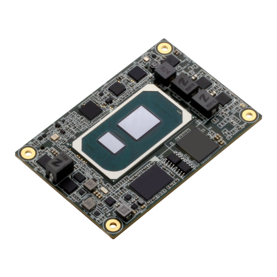
- Page 1 NanoCOM-TGU COM Express Module User’s Manual 2nd Ed Last Updated: November 23, 2021...
- Page 2 Copyright Notice This document is copyrighted, 2021. All rights are reserved. The original manufacturer reserves the right to make improvements to the products described in this manual at any time without notice. No part of this manual may be reproduced, copied, translated, or transmitted in any form or by any means without the prior written permission of the original manufacturer.
- Page 3 Acknowledgements All other products’ name or trademarks are properties of their respective owners. Microsoft Windows is a registered trademark of Microsoft Corp. Intel® and Celeron® are registered trademarks of Intel Corporation Intel Core™ is a trademark of Intel Corporation ...
- Page 4 Packing List Before setting up your product, please make sure the following items have been shipped: Item Quantity NanoCOM-TGU If any of these items are missing or damaged, please contact your distributor or sales representative immediately. Preface...
- Page 5 About this Document This User’s Manual contains all the essential information, such as detailed descriptions and explanations on the product’s hardware and software features (if any), its specifications, dimensions, jumper/connector settings/definitions, and driver installation instructions (if any), to facilitate users in setting up their product. Users may refer to the product page at AAEON.com for the latest version of this document.
- Page 6 Safety Precautions Please read the following safety instructions carefully. It is advised that you keep this manual for future references All cautions and warnings on the device should be noted. Make sure the power source matches the power rating of the device. Position the power cord so that people cannot step on it.
- Page 7 If any of the following situations arises, please the contact our service personnel: Damaged power cord or plug Liquid intrusion to the device iii. Exposure to moisture Device is not working as expected or in a manner as described in this manual The device is dropped or damaged Any obvious signs of damage displayed on the device...
- Page 8 FCC Statement This device complies with Part 15 FCC Rules. Operation is subject to the following two conditions: (1) this device may not cause harmful interference, and (2) this device must accept any interference received including interference that may cause undesired operation.
- Page 9 China RoHS Requirements (CN) 产品中有毒有害物质或元素名称及含量 AAEON Main Board/ Daughter Board/ Backplane 有毒有害物质或元素 部件名称 铅 汞 镉 六价铬 多溴联苯 多溴二苯醚 (Pb) (Hg) (Cd) (Cr(VI)) (PBB) (PBDE) 印刷电路板 × ○ ○ ○ ○ ○ 及其电子组件 外部信号 × ○ ○ ○ ○ ○ 连接器及线材...
- Page 10 China RoHS Requirement (EN) Poisonous or Hazardous Substances or Elements in Products AAEON Main Board/ Daughter Board/ Backplane Poisonous or Hazardous Substances or Elements Hexavalent Polybrominated Polybrominated Component Lead Mercury Cadmium Chromium Biphenyls Diphenyl Ethers (Pb) (Hg) (Cd) (Cr(VI)) (PBB) (PBDE) PCB &...
-
Page 11: Table Of Contents
Table of Contents Chapter 1 - Product Specifications..................1 Specifications ......................2 Chapter 2 – Hardware Information ..................4 Dimensions ....................... 5 Row A/B Connector Pin Definitions ..............7 Function Block Diagram ..................12 Chapter 3 - AMI BIOS Setup ....................13 System Test and Initialization ................14 AMI BIOS Setup ...................... - Page 12 3.5.5 Legacy Logical Devices Configuration ..........40 3.5.5.1 Serial Port 1 Configuration ...............41 3.5.5.2 Serial Port 2 Configuration ............. 42 3.5.6 Serial Port Console Redirection .............. 43 Setup Submenu: Security ..................44 3.6.1 Trusted Computing ..................45 3.6.2 Secure Boot ....................47 3.6.2.1 Key Management ................
-
Page 13: Chapter 1 - Product Specifications
Chapter 1 Chapter 1 - Product Specifications... -
Page 14: Specifications
Specifications System Form Factor COM Express Mini size, Type 10 11th Generation Intel® Core™ Series Processor CPU Frequency Up to 1.80 GHz, i7-1185GRE Chipset 11th Generation Intel® Core™ Series SoC Memory Type Onboard LPDDR4x-4266, in-band ECC support based on SKU Max. - Page 15 Display Display Controller Intel® UHD Graphics Video Output Dual Display: eDP, DDI x 1 Ethernet Intel® i225LM, up to 2.5 Gbps Ethernet x 1 Audio High Definition Audio Interface USB port USB3.2 Gen 2 x 2 USB2.0 x 8 Serial Port 2-wire UART (TX/RX) x 2 HDD Interface SATA III x 2...
-
Page 16: Chapter 2 - Hardware Information
Chapter 2 Chapter 2 – Hardware Information... -
Page 17: Dimensions
Dimensions Chapter 2 – Hardware Information... - Page 18 Chapter 2 – Hardware Information...
-
Page 19: Row A/B Connector Pin Definitions
Row A/B Connector Pin Definitions Row A Row B GND (FIXED) GND (FIXED) GBE0_MDI3- GBE0_ACT# GBE0_MDI3+ LPC_FRAME# GBE0_LINK100# LPC_AD0 GBE0_LINK1000# LPC_AD1 GBE0_MDI2- LPC_AD2 GBE0_MDI2+ LPC_AD3 GBE0_LINK# GBE0_MDI1- GBE0_MDI1+ LPC_CLK GND (FIXED) GND (FIXED) GBE0_MDI0- PWRBTN# GBE0_MDI0+ SMB_CK SMB_DAT SUS_S3# SMB_ALERT# SATA0_TX+ SATA1_TX+ SATA0_TX-... - Page 20 Row A Row B USB3_RX1_N USB3_TX1_N USB3_RX1_P USB3_TX1_P BATLOW# ATA_ACT# AC_SYNC AC_RST# AC_SDIN0 GND (FIXED) GND (FIXED) AC_BITCLK SPKR AC_SDOUT I2C_CK BIOS_DIS0# I2C_DAT THRMTRIP# THRM# USB6- USB7- USB6+ USB7+ USB_6_7_OC# USB_4_5_OC# USB4- USB5- USB4+ USB5+ GND (FIXED) GND (FIXED) USB2- USB3- USB2+ USB3+...
- Page 21 Row A Row B GND (FIXED) GND (FIXED) GPI0 GPO1 GPO2 PCIE_TX3+ PCIE_RX3+ PCIE_TX3- PCIE_RX3- GND (FIXED) GND (FIXED) PCIE_TX2+ PCIE_RX2+ PCIE_TX2- PCIE_RX2- GPI1 GPO3 PCIE_TX1+ PCIE_RX1+ PCIE_TX1- PCIE_RX1- WAKE0# GPI2 WAKE1# PCIE_TX0+ PCIE_RX0+ PCIE_TX0- PCIE_RX0- GND (FIXED) GND (FIXED) EDP_TX2_P DDI0_PAIR0+ EDP_TX2_N...
- Page 22 Row A Row B EDP_VDDEN EDP_BKLTEN GND (FIXED) GND (FIXED) EDP_TX3_P DDI0_PAIR3+ EDP_TX3_N DDI0_PAIR3- EDP_AUXP EDP_BKLT_CTRL EDP_AUXN VCC_5V_SBY GPI3 VCC_5V_SBY VCC_5V_SBY EDP_HPD VCC_5V_SBY PCIE0_CK_REF+ BISO_DIS1# PCIE0_CK_REF- DDI0_HPD GND (FIXED) GND (FIXED) SPI_POWER SPI_MISO GPO0 SPI_CLK SPI_MOSI DDI0_DDC_AUX_SEL TYPE10# SPI_CS# (Pull down 47k ohm to GND) RS1_TX DDI0_AUX_DP RS1_RX...
- Page 23 Row A Row B A103 LID# B103 SLEEP# A104 VCC_12V B104 VCC_12V A105 VCC_12V B105 VCC_12V A106 VCC_12V B106 VCC_12V A107 VCC_12V B107 VCC_12V A108 VCC_12V B108 VCC_12V A109 VCC_12V B109 VCC_12V A110 GND (FIXED) B110 GND (FIXED) Chapter 2 – Hardware Information...
-
Page 24: Function Block Diagram
Function Block Diagram Chapter 2 – Hardware Information... -
Page 25: Chapter 3 - Ami Bios Setup
Chapter 3 Chapter 3 - AMI BIOS Setup... -
Page 26: System Test And Initialization
System Test and Initialization The system uses certain routines to perform testing and initialization during the boot up sequence. If an error, fatal or non-fatal, is encountered, the system will output a few short beeps or an error message. The board can usually continue the boot up sequence with non-fatal errors. -
Page 27: Ami Bios Setup
AMI BIOS Setup The AMI BIOS ROM has a pre-installed Setup program that allows users to modify basic system configurations, which is stored in the battery-backed CMOS RAM and BIOS NVRAM so that the information is retained when the power is turned off. To enter BIOS Setup, press <Del>... -
Page 28: Setup Submenu: Main
Setup Submenu: Main Chapter 3 – AMI BIOS Setup... -
Page 29: Setup Submenu: Advanced
Setup Submenu: Advanced Chapter 3 – AMI BIOS Setup... -
Page 30: Graphics Configuration
3.4.1 Graphics Configuration Options Summary VBT Select eDP On eDP Off Optimal Default; Failsafe Default Select VBT for GOP Driver Chapter 3 – AMI BIOS Setup... -
Page 31: Cpu Configuration
3.4.2 CPU Configuration Options Summary Active Processor Optimal Default, Failsafe Default Cores Number of cores to enable in each processor package. Turbo Mode Disabled Enabled Optimal Default, Failsafe Default Enable/Disable processor Turbo Mode (requires EMTTM enabled too). AUTO means enabled Hyper-Threading Disabled Enabled... - Page 32 Options Summary Intel (VMX) Disabled Virtualization Enabled Optimal Default, Failsafe Default Technology When enabled, a VMM can utilize the additional hardware capabilities provided by Vanderpool Technology. Chapter 3 – AMI BIOS Setup...
-
Page 33: Memory Configuration
3.4.3 Memory Configuration Note: In-Band ECC Support availability depends on CPU. Options Summary In-Band ECC Disabled Support Enabled Optimal Default, Failsafe Default Enable/Disable In-Band ECC. Either the IBECC or the TME can be enabled In-Band ECC Error Enabled Injection Disabled Optimal Default, Failsafe Default By enabling this Error Injection feature, the user acknowledges the security risks. -
Page 34: On-Module H/W Monitor
3.4.4 On-Module H/W Monitor Chapter 3 – AMI BIOS Setup... -
Page 35: Fan 1 Mode Configuration
3.4.4.1 Fan 1 Mode Configuration Fan 1: Full Mode Options Summary FAN 1 Full Mode Optimal Default, Failsafe Default Manual Mode by PWM Auto Mode by PWM Smart Fan Mode Select PWM signal Non-inverting Optimal Default, Failsafe Default Inverting Select output PWM of inverting or non-inverting signal. Chapter 3 –... - Page 36 Fan 1: Manual Mode by PWM Options Summary Manual Setting Optimal Default; Failsafe Default Set Fan at fixed Duty-Cycle Min = 0 Max = 100 Please input Dec number: Chapter 3 – AMI BIOS Setup...
- Page 37 Fan 1: Auto Mode by PWM Options Summary Monitor Thermal CPU Temperature (PECI) Optimal Default, Failsafe Default Thermal Source 1(T1) Thermal Source 2(T2) Select monitor thermal source Temperature Of Start 30 Optimal Default, Failsafe Default Temperature Of Start Temperature of Off Optimal Default, Failsafe Default Temperature of Off Start PWM...
-
Page 38: Pch-Fw Configuration
3.4.5 PCH-FW Configuration Chapter 3 – AMI BIOS Setup... -
Page 39: Firmware Update Configuration
3.4.5.1 Firmware Update Configuration Options Summary Me FW Image Enabled Re-Flash Disabled Optimal Default, Failsafe Default Enable/Disable Me FW Image Re-Flash function. Local FW Update Enabled Optimal Default, Failsafe Default Disabled Enable/Disable ME FW Update function Chapter 3 – AMI BIOS Setup... -
Page 40: On-Module Configuration
3.4.6 On-Module Configuration Options Summary Battery Disabled Optimal Default, Failsafe Default Management One Battery Enable to support battery in ACPI OS by I2C_CK, I2C_DAT (B33, B34) EC-SMB-HC Enabled Support Disabled Optimal Default, Failsafe Default SMBus Host Controller Interface via Embedded Controller. Chapter 3 –... -
Page 41: Power Management
3.4.7 Power Management Options Summary Power Mode ATX Type Optimal Default, Failsafe Default AT Type Select system power mode. Restore AC Power Last State Loss Always On Always Off Optimal Default, Failsafe Default SIO Restore AC Power Loss: To decide the behavior after system power cut then resupply. -
Page 42: Aaeon Bios Robot
3.4.8 AAEON BIOS Robot Options Summary Sends watch dog Disabled Optimal Default, Failsafe Default before BIOS POST. Enabled Enabled - Robot set Watch Dog Timer (WDT) right after power on, before BIOS start POST process. And then Robot will clear WDT on completion of POST. WDT will reset system automatically if it is not cleared before its timer counts down to zero. - Page 43 Options Summary Delayed POST (DXE Disabled Optimal Default, Failsafe Default phase) Enabled Enabled – Robot holds BIOS from starting POST, right after power. This allows BIOS POST to start with stable power or start after system is physically warmed-up. Note: Robot does this before ‘Sends watch dog’. Reset System once Disabled Optimal Default, Failsafe Default Enabled...
-
Page 44: Setup Submenu: System I/O
Setup Submenu: System I/O Chapter 3 – AMI BIOS Setup... -
Page 45: Pci Express Configuration
3.5.1 PCI Express Configuration Options Summary PCI Express Root Disabled Port 1 Enabled Optimal Default, Failsafe Default Control the PCI Express Root Port. PCIe Speed Auto Optimal Default, Failsafe Default Gen1 Gen2 Gen3 Gen4 Configure PCIe Speed Hot Plug Disabled Optimal Default, Failsafe Default Enabled PCI Express Hot Plug Enable/Disable... - Page 46 Options Summary PCIe 0_3 Select PCIE Controller are four ×1 Optimal Default, Failsafe Default PCIE Controller are one ×2 and two ×1 PCIE Controller are two ×2 PCIE Controller is one ×4 PCIE Controller Selection PCI Express 0 Disable Enable Optimal Default, Failsafe Default Control the PCI Express Root Port.
- Page 47 Options Summary PCI Express 3 Disable Enable Optimal Default, Failsafe Default Control the PCI Express Root Port. PCIe Speed Auto Optimal Default, Failsafe Default Gen1 Gen2 Gen3 Configure PCIe Speed Hot Plug Disabled Optimal Default, Failsafe Default Enabled PCI Express Hot Plug Enable/Disable PCI Express 4 Disable Enable...
-
Page 48: Storage Configuration
3.5.2 Storage Configuration Options Summary SATA Controller(s) Enabled Optimal Default, Failsafe Default Disabled Enable/Disable SATA Device. Port 0 Disabled Enabled Optimal Default, Failsafe Default Enable or Disable SATA Port Hot Plug Disabled Optimal Default, Failsafe Default Enabled Designates this port as Hot Pluggable SATA Device Type Hard Disk Drive Optimal Default, Failsafe Default... - Page 49 Options Summary Hot Plug Disabled Optimal Default, Failsafe Default Enabled Designates this port as Hot Pluggable SATA Device Type Hard Disk Drive Optimal Default, Failsafe Default Solid State Drive Identify the SATA port is connected to Solid State Drive or Hard Disk Drive Chapter 3 –...
-
Page 50: Hd Audio Configuration
3.5.3 HD Audio Configuration Options Summary HD Audio Disabled Enabled Optimal Default, Failsafe Default Control Detection of the HD-Audio device. Disabled: HD-Audio will be unconditionally disabled. Enabled: HD-Audio will be unconditionally enabled. Chapter 3 – AMI BIOS Setup... -
Page 51: Digital Io Port Configuration
3.5.4 Digital IO Port Configuration Options Summary GPI* Output Input Optimal Default, Failsafe Default Set DIO as Input or Output GPO* Output Optimal Default, Failsafe Default Input Set DIO as Input or Output Output Level High Optimal Default, Failsafe Default Set output level when DIO pin is output Chapter 3 –... -
Page 52: Legacy Logical Devices Configuration
3.5.5 Legacy Logical Devices Configuration Chapter 3 – AMI BIOS Setup... -
Page 53: Serial Port 1 Configuration
3.5.5.1 Serial Port 1 Configuration Options Summary Use This Device Disabled Enabled Optimal Default, Failsafe Default Enable or Disable this Logical Device. Possible Use Automatic Settings Optimal Default, Failsafe Default IO=3F8h; IRQ=4; DMA; IO=2C8h; IRQ=11; DMA Allows the user to change the device resource settings. New settings will be reflected on this setup page after system restarts. -
Page 54: Serial Port 2 Configuration
3.5.5.2 Serial Port 2 Configuration Options Summary Use This Device Disabled Enabled Optimal Default, Failsafe Default Enable or Disable this Logical Device. Possible Use Automatic Settings Optimal Default, Failsafe Default IO=2F8h; IRQ=3; DMA; IO=2D8h; IRQ=10; DMA Allows the user to change the device resource settings. New settings will be reflected on this setup page after system restarts. -
Page 55: Serial Port Console Redirection
3.5.6 Serial Port Console Redirection Options Summary Console Redirection Disabled Optimal Default, Failsafe Default Enabled Console Redirection Enable or Disable. Console Redirection Disabled Optimal Default, Failsafe Default Enabled Console Redirection Enable or Disable. Chapter 3 – AMI BIOS Setup... -
Page 56: Setup Submenu: Security
Setup Submenu: Security Change User/Administrator Password You can set an Administrator Password or User Password. An Administrator Password must be set before you can set a User Password. The password will be required during boot up, or when the user enters the Setup utility. A User Password does not provide access to many of the features in the Setup utility. -
Page 57: Trusted Computing
3.6.1 Trusted Computing Options Summary Security Device Disable Optimal Default, Failsafe Default Support Enable Enables or Disables BIOS support for security device. O.S. will not show Security Device. TGU EFI protocol and INT1A interface will not be available. SHA-1 PCR Bank Disabled Optimal Default, Failsafe Default Enabled... - Page 58 Options Summary SM3_256 PCR Bank Disabled Optimal Default, Failsafe Default Enabled Enable or Disable SM3_256 PCR Bank Pending operation None Optimal Default, Failsafe Default TPM Clear Schedule an Operation for the Security Device. Note: Your Computer will reboot during restart in order to change State of Security Device. Platform Hierarchy Disabled Enabled Optimal Default, Failsafe Default...
-
Page 59: Secure Boot
3.6.2 Secure Boot Options Summary Secure Boot Disabled Optimal Default, Failsafe Default Enabled Secure Boot feature is Active if Secure Boot is Enabled, Platform Key (PK) is enrolled and the System mode is in User mode. Changing the mode requires platform reset. Secure Boot Mode Standard Optimal Default, Failsafe Default Custom... -
Page 60: Key Management
3.6.2.1 Key Management Options Summary Factory Key Disabled Optimal Default, Failsafe Default Provision Enabled Install factory default Secure Boot keys after the platform reset and while the System is in Setup mode. Chapter 3 – AMI BIOS Setup... -
Page 61: Setup Submenu: Boot
Setup Submenu: Boot Options Summary Quiet Boot Disabled Enabled Optimal Default, Failsafe Default Enables or disables Quiet Boot option. Network Stack Disabled Optimal Default, Failsafe Default Enabled Enable/ Disable UEFI Network Stack Chapter 3 – AMI BIOS Setup... -
Page 62: Setup Submenu: Save & Exit
Setup Submenu: Save & Exit Chapter 3 – AMI BIOS Setup... -
Page 63: Chapter 4 - Drivers Installation
Chapter 4 Chapter 4 – Drivers Installation... -
Page 64: Driver Download And Installation
Driver Download and Installation Drivers for the NanoCOM-TGU can be downloaded from the product page on the AAEON website by following this link: https://www.aaeon.com/en/p/com-express-cpu-modules-nanocom-tgu Download the driver(s) you need and extract the zip. Then, follow the steps below to install the drivers. Audio Driver (Windows 10) Open the folder where you unzipped the Audio Drivers Run the Setup.exe in the folder... - Page 65 LAN Drivers (Windows 10) Open the folder where you unzipped the LAN Drivers Read the ReadMe.txt file before proceeding. Caution: Be sure to install the driver package before installing the Intel® PROSet package. Open the Wired_driver_26.3_x64 folder Run the Wired_driver_26.3_x64.exe file in the folder Follow the instructions, drivers will be installed automatically.
- Page 66 Peripheral Driver (Linux) Open the folder where you unzipped the Peripheral Drivers Follow the instructions contained within the user guides to install the related drivers. Chapter 4 – Driver Installation...
-
Page 67: Appendix A - Watchdog Timer Programming
Appendix A Appendix A - Watchdog Timer Programming... -
Page 68: Watchdog Timer Initial Program
Watchdog Timer Initial Program Table 1: Embedded BRAM relative register table Default Value Note Index 0x284(Note1) BRAM Index Register Data 0x285(Note2) BRAM Data Register Logical Device Number 0xA8(Note3) Watch dog Logical Device Number Function and Device Number 0x00(Note4) Watch dog Function/Device Number Table 2: Watchdog relative register table Option Register BitNum... - Page 69 ************************************************************************************ // Embedded BRAM relative definition (Please reference to Table 1) #define byte EcBRAMIndex //This parameter is represented from Note1 #define byte EcBRAMData //This parameter is represented from Note2 #define byte BRAMLDNReg //This parameter is represented from Note3 #define byte BRAMFnDataReg //This parameter is represented from Note4 #define void EcBRAMWriteByte(byte Offset, byte Value);...
- Page 70 ************************************************************************************ Main VOID // Procedure : AaeonWDTConfig // (byte)Timer : Time of WDT timer.(0x00~0xFF) // (boolean)Unit : Select time unit(0: second, 1: minute). AaeonWDTConfig(); // Procedure : AaeonWDTEnable // This procudure will enable the WDT counting. AaeonWDTEnable(); ************************************************************************************ Appendix A – Watchdog Timer Programming...
- Page 71 ************************************************************************************ // Procedure : AaeonWDTEnable AaeonWDTEnable () VOID WDTEnableDisable( // Procedure : AaeonWDTConfig AaeonWDTConfig () VOID // Disable WDT counting WDTEnableDisable( // WDT relative parameter setting WDTParameterSetting(); WDTEnableDisable(byte Value) VOID ECBRAMWriteByte(TimerReg , Value); WDTParameterSetting() VOID Byte TempByte; // Watchdog Timer counter setting ECBRAMWriteByte(TimerReg , TimerVal);...
- Page 72 ************************************************************************************ ECBRAMWriteByte(byte OPReg, byte OPBit, byte Value) VOID IOWriteByte(EcBRAMIndex, 0x10); IOWriteByte(EcBRAMData, BRAMLDNReg); IOWriteByte(EcBRAMIndex, 0x11); IOWriteByte(EcBRAMData, BRAMFnDataReg); IOWriteByte(EcBRAMIndex, 0x13 + OPReg); IOWriteByte(EcBRAMData, Value); IOWriteByte(EcBRAMIndex, 0x12); IOWriteByte(EcBRAMData, 0x30); //Write start ECBRAMReadByte(byte OPReg) Byte IOWriteByte(EcBRAMIndex, 0x10); IOWriteByte(EcBRAMData, BRAMLDNReg); IOWriteByte(EcBRAMIndex, 0x11); IOWriteByte(EcBRAMData, BRAMFnDataReg); IOWriteByte(EcBRAMIndex, 0x12); IOWriteByte(EcBRAMData, 0x10);...
-
Page 73: Appendix B - I/O Information
Appendix B Appendix B - I/O Information... -
Page 74: I/O Address Map
I/O Address Map Appendix B – I/O Information... - Page 75 Appendix B – I/O Information...
-
Page 76: Memory Address Map
Memory Address Map Appendix B – I/O Information... -
Page 77: Large Memory Address Map
Large Memory Address Map Appendix B – I/O Information... -
Page 78: Irq Mapping Chart
IRQ Mapping Chart Appendix B – I/O Information... - Page 79 Appendix B – I/O Information...
- Page 80 Appendix B – I/O Information...
- Page 81 Appendix B – I/O Information...
- Page 82 Appendix B – I/O Information...
- Page 83 Appendix B – I/O Information...
- Page 84 Appendix B – I/O Information...
- Page 85 Appendix B – I/O Information...
- Page 86 Appendix B – I/O Information...
- Page 87 Appendix B – I/O Information...
- Page 88 Appendix B – I/O Information...
-
Page 89: Appendix C - Programming Digital I/O
Appendix C Appendix C – Programming Digital I/O... -
Page 90: Dio Programming
DIO Programming NanoCOM-TGU utilizes an AAEON chipset as its Digital I/O controller. Below are the procedures to complete its configuration which you can use to develop a customized program to fit your application. Appendix C –Programming Digital I/O... -
Page 91: Digital I/O Register
Digital I/O Register Table 1: Embedded BRAM relative register table Default Value Note Index 0x284(Note1) BRAM Index Register Data 0x285(Note2) BRAM Data Register Logical Device Number 0xA2(Note3) Watch dog Logical Device Number IO Direction DIO Input/Output Function/Device 0x00(Note4) Function and Device Number Number IO Value/Status DIO Output Data Function/Device... -
Page 92: Digital I/O Sample Program
Digital I/O Sample Program ************************************************************************************ // Embedded BRAM relative definition (Please reference to Table 1) #define byte EcBRAMIndex //This parameter is represented from Note1 #define byte EcBRAMData //This parameter is represented from Note2 #define byte BRAMLDNReg //This parameter is represented from Note3 #define byte BRAMFnData0Reg //This parameter is represented from Note4 #define byte... - Page 93 ************************************************************************************ Main VOID Boolean PinStatus ; // Procedure : AaeonReadPinStatus // Input : Example, Read Digital I/O Pin 3 status // Output : InputStatus : 0: Digital I/O Pin level is low 1: Digital I/O Pin level is High PinStatus = AaeonReadPinStatus(DIO0ToDIO7Reg, DIO3Bit); // Procedure : AaeonSetOutputLevel // Input : Example, Set Digital I/O Pin 6 level...
- Page 94 ************************************************************************************ AaeonReadPinStatus(byte OptionReg, byte BitNum) Boolean Byte TempByte; TempByte = ECBRAMReadByte(BRAMFnData1Reg, OptionReg); If (TempByte & BitNum == 0) Return 0; Return 1; AaeonSetOutputLevel(byte OptionReg, byte BitNum, byte Value) VOID Byte TempByte; TempByte = ECBRAMReadByte(BRAMFnData1Reg, OptionReg); TempByte |= (Value << BitNum); ECBRAMWriteByte(OptionReg, BitNum, Value);...
- Page 95 ************************************************************************************ ECBRAMWriteByte(byte OPReg, byte OPBit, byte Value) VOID IOWriteByte(EcBRAMIndex, 0x10); IOWriteByte(EcBRAMData, BRAMLDNReg); IOWriteByte(EcBRAMIndex, 0x11); IOWriteByte(EcBRAMData, BRAMFnDataReg); IOWriteByte(EcBRAMIndex, 0x13 + OPReg); IOWriteByte(EcBRAMData, Value); IOWriteByte(EcBRAMIndex, 0x12); IOWriteByte(EcBRAMData, 0x30); //Write start ECBRAMReadByte(byte FnDataReg, byte OPReg) Byte IOWriteByte(EcBRAMIndex, 0x10); IOWriteByte(EcBRAMData, BRAMLDNReg); IOWriteByte(EcBRAMIndex, 0x11); IOWriteByte(EcBRAMData, FnDataReg); IOWriteByte(EcBRAMIndex, 0x12);...