Table of Contents
Advertisement
Quick Links
Advertisement
Table of Contents

Related Manuals for LG Flatron L1811B


Summary of Contents for LG Flatron L1811B
- Page 1 Website:http://biz.LGservice.com E-mail:http://www.LGEservice.com/techsup.html COLOR MONITOR SERVICE MANUAL CHASSIS NO. : CL-29 FACTORY MODEL: LB801H MODEL: L1811B(LB801H-GL) ) ID LABEL MODEL No. CAUTION BEFORE SERVICING THE UNIT, READ THE SAFETY PRECAUTIONS IN THIS MANUAL. L1811B...
-
Page 2: Table Of Contents
CONTENTS SPECIFICATIONS ........... 2 ADJUSTMENT ............12 PRECAUTIONS ............4 TROUBLESHOOTING GUIDE ......13 TIMING CHART ............5 PRINTED CIRCUIT BOARD........18 OPERATING INSTRUCTIONS ........ 6 EXPLODED VIEW...........22 WIRING DIAGRAM ..........8 REPLACEMENT PARTS LIST .......24 BLOCK DIAGRAM ........... 9 PIN CONFIGURATION..........30 DESCRIPTION OF BLOCK DIAGRAM....10 SCHEMATIC DIAGRAM ......... - Page 3 Signal Connector Pin Assignment • DVI-I Connector (Digital/Analog) Signal (DVI-I) Signal (DVI-I) T. M. D. S. Data2- Hot Plug Detect T. M. D. S. Data0- T. M. D. S. Data2+ T. M. D. S. Data2/4 Shield T. M. D. S. Data0+ T.
-
Page 4: Precautions
PRECAUTION WARNING FOR THE SAFETY-RELATED COMPONENT. WARNING BE CAREFUL ELECTRIC SHOCK ! • There are some special components used in LCD monitor that are important for safety. These parts are • If you want to replace with the new backlight (CCFL) or marked on the schematic diagram and the inverter circuit, must disconnect the AC adapter... -
Page 5: Timing Chart
TIMING CHART VIDEO SYNC << Dot Clock (MHz), Horizontal Frequency (kHz), Vertical Frequency (Hz), Horizontal etc... (µs), Vertical etc... (ms) >> Total Period Video Active Time Front Porch Sync Duration Back Porch Sync Mode Resolution Frequency Clock Sort Polarity 31.469 640x350 25.175 70Hz... -
Page 6: Operating Instructions
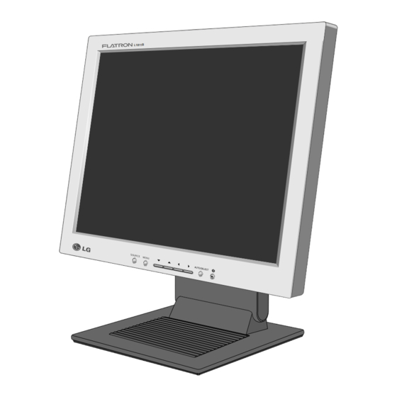
OPERATING INSTRUCTIONS FRONT VIEW REAR VIEW L1811B Power Connect Front Control Panel USB Port D-Sub Signal DVI Connect Connect Front Control Panel 1. Power ON/OFF Button Button ▼▲◀▶ Use this button to turn the monitor on or off. Use these buttons to choose or adjust items in the On Screen Display. - Page 7 Making use of USB (Universal Serial Bus)* USB (Universal Serial Bus) is an innovation in connecting your different desktop peripherals conveniently to your computer. By using the USB, you will be able to connect your mouse, keyboard, and other to your monitor instead of having to connect them to your computer.
-
Page 8: Wiring Diagram
WIRING DIAGRAM 6631T25008Q Connector Ass’y P/N: MAIN PCB Connector Ass’y P/N: 6631T20015R P902 J705 MATAL FRAME J801 J702 J710 Connector Ass’y P/N: 6631T20008U CN_C02 CN_C01 CN301 MODULE 6631T11012P Connector Ass’y P/N: - 8 -... -
Page 9: Block Diagram
BLOCK DIAGRAM Power Board - 9 -... -
Page 10: Description Of Block Diagram
DESCRIPTION OF BLOCK DIAGRAM 1. Input signal switching part(BA7657). There are two anolog inputs which are D-Sub analog and DVI-anolog input. They come from each 15 pin D-Sub and 29 pin DVI-I connector. 2. Video Controller Part(GM5020). This part amplifies the level of video signal for the anolog to digital conversion and converts from the analog video signal to the digital video signal using a pixelclock. - Page 11 50 ~ 60Hz 100KHz HVDC INPUT RECTIFIER ENERGY OUTPUT RECTIFIER COMPONENTS AND FILTER TRANSFER AND FILTER LINE 100 ~ 240V PWM CONTROL PHOTO-COUPLER SIGNAL CIRCUIT ISOLATION COLLECTION SECONDA RY PRIMARY Operation description_Power 1. EMI components. This part contains of EMI components to comply with global marketing EMI standards like FCC, VCCI CISPR, the circuit included a line-filter, across line capacitor and of course the primary protection fuse.
-
Page 12: Adjustment
ADJUSTMENT All adjustment are thoroughly checked and corrected 3. Adjustment for White Balance when the monitor leaves the factory, but sometimes 1) Display color 0,0 pattern at Mode 15. several minor adjustment may be required. 2) Set External Bright to MAX position and Contrast to Adjustment should be following procedure and after MAX Position. -
Page 13: Troubleshooting Guide
TROUBLESHOOTING GUIDE 1. NO POWER NO POWER (POWER INDICATOR OFF) CHECK J801 TROUBLE IN INPUT VOLTAGE BULT-IN POWER (12V) ? CHECK J801 TROUBLE IN 5VST VOLTAGE BULT-IN POWER (5V) ? CHECK U501’s PIN 6. TROUBLE IN IS THIS PIN U501 or X501 OSCILLATED? TROUBLE SOMEWHERE ELSE... - Page 14 2. NO RASTER NO RASTER CHECK TROUBLE IN J702 PIN 1, 2, 3 POWER ADATER (12V) ? or L703, L704 CHECK TROUBLE IN J702 PIN 8 (5V) ? INVON PATTERN CHECK TROUBLE IN X501 X501 H. PULSE ? CHECK TROUBLE IN U201(GM5020) ? U201 CHECK...
- Page 15 CHECK TROUBLE IN L204 U201 PULSE ? CHECK CHECK DOT CLOCK U401 PIN 10 PATTERN PULSE ? CHECK CHECK U401 PIN 8 V.PULSE? DVS PATTERN CHECK CHECK U401 PIN 7 DHS PATTERN V.PULSE? TROUBLE IN LCD MODULE - 15 -...
- Page 16 3. NO CLOCK (CLOCK GENERATOR) NO DOT CLOCK CHECK TROUBLE IN X201 24MHz ? X201 CHECK TROUBLE IN L201 U201 CLOCK ? - 16 -...
- Page 17 4. TROUBLE IN DPM TROUBLE IN DPM CHECK PC CHECK PC IS NOT GOING R233, R234? INTO DPM OFF MODE CHECK U501 PIN 6 TROUBLE IN WAVEFORM X501 (24MHz) ? CHECK TROUBLE IN U501 PIN 11 SIGNAL CABLE (0V) ? TROUBLE IN PC - 17 -...
-
Page 18: Printed Circuit Board
PRINTED CIRCUIT BOARD 1. MAIN BOARD (Component Side) L820 L810 J705 J801 U802 L821 C817 J702 C845 C850 L811 R809 C531 C844 R810 U503 C701 C526 C409 C840 R581 R745 C834 C516 U821 R406 U401 R701 R514 R543 L402 C706 R542 R544 C410... - Page 19 2. MAIN BOARD (Solder Side) L703 L704 R201 C214 C222 C223 C212 C207 R239 R240 D741 D701 D704 D714 D715 D740 R752 D746 D744 D747 D745 D730 D731 - 19 -...
- Page 20 3. POWER BOARD (Component Side) 4. POWER BOARD (Solder Side) - 20 -...
- Page 21 5. CONTROL BOARD 6.USB BOARD - 21 -...
-
Page 22: Exploded View
EXPLODED VIEW - 22 -... - Page 23 Description Ref. No. Part No. CABINET ASSEMBLY, LB801H BRAND 3090TKL045 .. 3091TKL044A LCD(LIQUID CRYSTAL DISPLAY), LM181E05-C4M1 LG PHILPS TFT COLOR 18.1" SXGA 6304FLP023A or 6304FLP004A LCD(LIQUID CRYSTAL DISPLAY), LM181E05-C3M1 LG PHILPS TFT COLOR 18.1" W/O BACK COVER ASSEMBLY, LB800H L030A 3809TKL025A TILT SWIVEL ASSEMBLY, LB800H .
-
Page 24: Replacement Parts List
REPLACEMENT PARTS LIST CAUTION: BEFORE REPLACING ANY OF THESE COMPONENTS, READ CAREFULLY THE SAFETY PRECAUTIONS IN THIS MANUAL. * NOTE SAFETY Mark AL ALTERNATIVE PARTS DATE: 2002. 04. 26. DATE: 2002. 04. 26. *S *AL LOC. NO. PART NO. DESCRIPTION / SPECIFICATION *S *AL LOC. - Page 25 DATE: 2002. 04. 26. DATE: 2002. 04. 26. *S *AL LOC. NO. PART NO. DESCRIPTION / SPECIFICATION *S *AL LOC. NO. PART NO. DESCRIPTION / SPECIFICATION C410 0CE107WF6DC 100UF MVK 16V 20% R/TP(SMD) C842 0CK103CK51A 0.01UF 1608 50V 10% R/TP B(Y C411 0CK103CK51A 0.01UF 1608 50V 10% R/TP B(Y...
- Page 26 DATE: 2002. 04. 26. DATE: 2002. 04. 26. *S *AL LOC. NO. PART NO. DESCRIPTION / SPECIFICATION *S *AL LOC. NO. PART NO. DESCRIPTION / SPECIFICATION U201 0IPRPGN001A GM5020 GENESIS 292P,PBGA TRA R145 0RJ0222D677 22 OHM 1/10 W 5% 1608 R/TP U301 0IEB121616A M12L16161A-7T 50P TSOP ST 16...
- Page 27 DATE: 2002. 04. 26. DATE: 2002. 04. 26. *S *AL LOC. NO. PART NO. DESCRIPTION / SPECIFICATION *S *AL LOC. NO. PART NO. DESCRIPTION / SPECIFICATION R525 0RJ1000D677 100 OHM 1/10 W 5% 1608 R/TP R766 0RJ0752D677 75 OHM 1/10 W 5% 1608 R/TP R526 0RJ1000D677 100 OHM 1/10 W 5% 1608 R/TP...
- Page 28 DATE: 2002. 04. 26. DATE: 2002. 04. 26. *S *AL LOC. NO. PART NO. DESCRIPTION / SPECIFICATION *S *AL LOC. NO. PART NO. DESCRIPTION / SPECIFICATION POWER BOARD R927 0RD0102A609 10 OHM 1/2 W (7.0) 5% TA52 C901 0CBZTBU002B BULK PCX2 335 474K R928 0RD0202Q609 20 1/4W(3 5% TA52...
- Page 29 DATE: 2002. 04. 26. *S *AL LOC. NO. PART NO. DESCRIPTION / SPECIFICATION 0RJ0222D677 22 OHM 1/10 W 5% 1608 R/TP 0RJ1502D677 15K OHM 1/10 W 5% 1608 R/TP 0RJ1502D677 15K OHM 1/10 W 5% 1608 R/TP 0RJ0000D677 0 OHM 1/10 W 5% 1608 R/TP 0RJ1002D677 10K OHM 1/10 W 5% 1608 R/TP 0RJ0222D677...
-
Page 30: Pin Configuration
PIN CONFIGURATION GM5020 GENESIS 292P FUNCTIONAL BLOCK DIAGRAM Serial I/F SDRAM/I/F Host Micro- Frame Store Interface processor Interface Anolog Triple YUV to RGB Output Converter Image Panel I/F Digital Zoom/ Data Frame Rate TMDS Caputure/ Gamma [48-bits] TMDS Brightness, Shrink/ Path/ Conversion Measure. - Page 31 CAT24WC08J-TE13 8P BLOCK DIAGRAM DIP Package(p) SOIX Package(J) EXTERNAL LOAD V CC V CC SENSE AMPS D OUT SHIFT REGISTERS V SS V SS V CC COLUMN V SS WORD ADDRESS BUFFERS DECODERS TSSOP Package(U) START/STOP LOGIC V CC E PROM XDEC V SS CONTROL...
-
Page 32: Schematic Diagram
SCHEMATIC DIAGRAM 1. GM5020 - 32 -... - Page 33 2. MEMORY - 33 -...
- Page 34 3. LVDS - 34 -...
- Page 35 4. MICOM - 35 -...
- Page 36 5. DC/DC - 36 -...
- Page 37 6. CONNECTOR - 37 -...
- Page 38 7. INPUT SWITCHING - 38 -...
- Page 39 8. CONTROL KEY - 39 -...
- Page 40 9.USB - 40 -...
- Page 41 10. POWER - 41 -...
- Page 42 May. 2002 P/NO : 3828TSL082C Printed in Korea...