
Related Manuals for Motorola PRPMC750


Summary of Contents for Motorola PRPMC750
- Page 1 sales@artisantg.com artisantg.com (217) 352-9330 | Visit our website - Click HERE...
- Page 2 PRPMC750 Processor PMC Module Installation and Use Manual PRPMC750A/IH2 May 2000...
- Page 3 The table below has been changed to reflect 8M Flash for all model numbers. The minimum air flow requirement has been changed from 150 LFM to 450 LFM, see Airflow Requirements on page B-1. The information contained in this manual applies to the PrPMC750 board, in the following model configurations: Model Number CPU/Speed...
- Page 4 PowerPC , PowerPC 603 , and PowerPC 604 are trademarks of IBM Corp, and are used by Motorola, Inc. under license from IBM Corp. is a trademark of IBM Corp. Timekeeper and Zeropower are trademarks of Thompson Components. All other products mentioned in this document are trademarks or registered trademarks of...
- Page 5 The safety precautions listed below represent warnings of certain dangers of which Motorola is aware. You, as the user of the product, should follow these warnings and all other safety precautions necessary for the safe operation of the equipment in your operating environment.
- Page 6 Flammability All Motorola PWBs (printed wiring boards) are manufactured with a flammability rating of 94V-0 by UL-recognized manufacturers. EMI Caution This equipment generates, uses and can radiate electromagnetic energy. It may cause or be susceptible to electromagnetic interference (EMI) if not installed and used CAUTION with adequate EMI protection.
- Page 7 While reasonable efforts have been made to assure the accuracy of this document, Motorola, Inc. assumes no liability resulting from any omissions in this document, or from the use of the information obtained therein. Motorola reserves the right to revise this document and to make changes from time to time in the content hereof without obligation of Motorola to notify any person of such revision or changes.
- Page 8 (b)(3) of the Rights in Technical Data clause at DFARS 252.227-7013 (Nov. 1995) and of the Rights in Noncommercial Computer Software and Documentation clause at DFARS 252.227-7014 (Jun. 1995). Motorola, Inc. Computer Group 2900 South Diablo Way Tempe, Arizona 85282...
- Page 9 Comments and Suggestions Motorola welcomes and appreciates your comments on its documentation. We want to know what you think about our manuals and how we can make them better. Mail comments Motorola Computer Group Reader Comments DW164 2900 S. Diablo Way...
- Page 10 Conventions Used in This Manual The following typographical conventions are used in this document: bold is used for user input that you type just as it appears; it is also used for commands, options and arguments to commands, and names of programs, directories and files. italic is used for names of variables to which you assign values.
-
Page 11: Table Of Contents
Unpacking the PrPMC750 Hardware ................1-5 Preparing the PrPMC750 Hardware ................1-5 PrPMC750 Configuration ...................1-5 Installation........................1-8 ESD Precautions ....................1-8 Installation of PrPMC750 on a VME or CompactPCI Board......1-8 Installation of Optional SDRAM Mezzanine on PrPMC750 ......1-11 CHAPTER 2 Operating Instructions Introduction........................2-1 Applying Power ......................2-1 PrPMC750........................2-2... - Page 12 Optional Memory Mezzanines ..............3-8 SROM....................... 3-11 System Registers ....................3-11 Timers....................... 3-11 32-Bit Timers .................... 3-11 Watchdog Timers ..................3-12 Interrupt Routing and Generation..............3-12 Asynchronous Serial Port ................. 3-13 Clock Generator ....................3-13 Processor Core Power Supply ................3-13 PCI Interface.....................
- Page 13 Overview........................6-1 CNFG - Configure Board Information Block ............6-2 ENV - Set Environment .....................6-3 Configuring the PPCBug Parameters ..............6-3 APPENDIX A Related Documentation Motorola Computer Group Documents ..............A-1 Manufacturers’ Documents..................A-3 Related Specifications....................A-6 APPENDIX B Specifications Specifications ......................B-1 Mechanical Characteristics ................B-1 Electrical Characteristics ...................
- Page 14 List of Figures Figure 1-1. PrPMC750 Headers, Connectors and Components.........1-7 Figure 1-2. Installing a PrPMC750 on a VMEmodule ..........1-10 Figure 1-3. Installing SDRAM Mezzanine on PrPMC750 ........1-12 Figure 2-1. PrPMC750 DEBUG Serial Port Configuration........2-4 Figure 3-1. PrPMC750 Block Diagram ..............3-4...
- Page 15 Table 4-6. J1 Debug Header Pin Assignments............4-11 Table 5-1. Debugger Commands ................5-7 Table 5-2. Diagnostic Test Groups ................5-11 Table A-1. Motorola Computer Group Documents ..........A-2 Table A-2. Manufacturers’ Documents ..............A-3 Table A-3. Related Specifications ................A-5 Table B-1. PrPMC750 Specifications ............... B-2 Table B-2.
-
Page 16: Introduction
Module and instructions for preparing and installing the hardware including the optional SDRAM memory mezzanine module. In this manual, the name PrPMC750 refers to all models of the PrPMC750 series boards unless otherwise specified. These are add-on modules intended for use with any host carrier board that will accept a PMC or processor PMC module. -
Page 17: Monarch And Non-Monarch Processor Pmcs
A system may have one Monarch PrPMC750 and/or one or more Non- monarch PrPMC750s, creating a loosely coupled multiprocessing system. A PrPMC750 operating as a Monarch may be mated to a carrier board with slave processors, PCI, and other I/O devices. A PrPMC750 operating as a Non-monarch may be installed on a carrier with a host processor and other PCI devices, such as an MVME2400 or an MCPN750 board. -
Page 18: System Enclosure
PrPMC750 (in a VME or CompactPCI chassis). The exception would be if the PrPMC750 contained the optional memory mezzanine board, which would place the entire PrPMC750 package 5.3mm over the allowed limit for a single slot, thereby requiring... - Page 19 A-1 Preparing the PrPMC750 Hardware Program the PrPMC750 module on page 1-5 and PMCs as needed for your You may also wish to obtain the PRPMC750 applications Programmer’s Reference Guide, listed in Appendix A, Related Documentation on page A-1...
-
Page 20: Unpacking The Prpmc750 Hardware
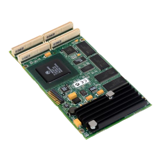
PrPMC750 Configuration The PrPMC750 provides software control over most options. By setting bits in control registers after installing the PrPMC750 in a system, you can modify its configuration. The PrPMC750 control registers are described in the PRPMC750 Processor PMC Module Programmer’s Reference Guide... - Page 21 Preparation and Installation Figure 1-1 illustrates the placement of connectors and LED indicators on the PrPMC750. The PrPMC750 has been factory tested and is shipped with the configurations described in the following sections. It contains a factory-installed debug monitor, PPCBug, which operates with those factory settings.
-
Page 22: Figure 1-1. Prpmc750 Headers, Connectors And Components
Preparing the PrPMC750 Hardware Figure 1-1. PrPMC750 Headers, Connectors, and Components http://www.motorola.com/computer/literature... -
Page 23: Installation
Preparation and Installation Installation The following instructions tell how to install the PrPMC750 on a typical VME or CompactPCI single board computer and how to install the optional memory mezzanine module on the PrPMC750. ESD Precautions Motorola strongly recommends that you use an antistatic wrist strap and a conductive foam pad when installing or upgrading a system. - Page 24 Avoid touching areas of integrated circuitry; static discharge can damage the circuits. Caution 4. Place the PrPMC750 mezzanine module on top of the VMEmodule, or CompactPCI board, with the four PMC connectors on the PrPMC750 aligned with the four corresponding connectors on the baseboard.
-
Page 25: Figure 1-2. Installing A Prpmc750 On A Vmemodule
Preparation and Installation Figure 1-2. Installing a PrPMC750 on a VMEmodule 5. Align the standoffs on the PrPMC750 mezzanine with the VMEmodule or CompactPCI board and install the phillips-head screws through the holes in the base board and the spacers. Tighten the screws. -
Page 26: Installation Of Optional Sdram Mezzanine On Prpmc750
Installation of Optional SDRAM Mezzanine on PrPMC750 The optional SDRAM mezzanine mounts on the backside (side 2) of the PrPMC750 processor module. (Note: this is possible only on a PrPMC750 assembled with the J2 memory expansion connector.) To install an SDRAM mezzanine, refer to Figure 1-3 and proceed as follows: 1. -
Page 27: Figure 1-3. Installing Sdram Mezzanine On Prpmc750
Figure 1-3. Installing SDRAM Mezzanine on PrPMC750 3. Carefully remove the VME or CompactPCI board, with the PrPMC750 installed, from its card slot and place it on a clean and adequately protected working surface (preferably an ESD mat), component side up, with the front panel facing you. Note that the ESD mat should be on a firm surface which does not bow. - Page 28 Installation 4. Remove four short phillips-head screws attached to the four stand- offs, from the side of the PrPMC750 facing up. Do not remove the PrPMC750 from the carrier board. 5. Pick up the SDRAM mezzanine module and note the position of the SDRAM connector P1.
- Page 29 Preparation and Installation Notes When the combined PrPMC750 and memory mezzanine is installed on a VME or CompactPCI board, the total assembly violates the single board height limit. In these situations, the adjacent VME or CompactPCI slot must be left vacant for proper installation and system use.
-
Page 30: Introduction
PPCBug firmware at power-up or system reset. The firmware initializes the devices on the PrPMC750 module in preparation for booting the operating system. The firmware is shipped from the factory with an appropriate set of defaults. -
Page 31: Prpmc750
Default is no boot. Interactive, command-driven on-line PowerPC MONITOR debugger, when terminal connected. PrPMC750 The status indicators (LEDs) and the Debug Serial port of the PrPMC750 are described in the following sections. Computer Group Literature Center Web Site... -
Page 32: Status Indicators
A three wire Debug serial RS232 port (TXD, RXD, GND) is available on the 2mm, 20-pin right-angle header (J1), located on the primary side of the PrPMC750. Refer to Figure 2-1 for pin definitions. An optional J1 to DB9 adapter cable is available from Motorola. Contact your local Motorola Sales Office for more information or to order. -
Page 33: Figure 2-1. Prpmc750 Debug Serial Port Configuration
Operating Instructions SOUT 16C550 Debug PrPMC750 Header J1 Figure 2-1. PrPMC750 DEBUG Serial Port Configuration Computer Group Literature Center Web Site... -
Page 34: Figure 3-1. Prpmc750 Block Diagram
This chapter describes the PrPMC750 Processor PMC Module on a block diagram level. The General Description on page 3-4 provides an overview of the PrPMC750, followed by a detailed description of several blocks of circuitry. Figure 3-1, PrPMC750 Block Diagram on page 3-5 shows a block diagram of the overall board architecture. -
Page 35: Chapter 3 Functional Description
Functional Description Features The following table summarizes the features of the PrPMC750 processor module. Table 3-1. PrPMC750 Features Feature Description Processor Single MPC750 Processor Core Frequency up to 366 MHz Bus Clock Frequencies up to 100 MHz. Address and data bus parity... - Page 36 Features Table 3-1. PrPMC750 Features (Continued) Feature Description PCI Interface 32/64-bit Data 33 MHz 3.3V/5V universal signaling interface P11, P12, P13 and P14 PMC connectors Address/data parity per PCI specification Form Factor Single width, standard length PMC (74mm x 149 mm) Height above carrier board: Standard - 13.5mm...
-
Page 37: General Description
MONARCH# signal from the PMC connector. When configured as the Monarch, the PrPMC750 will enumerate the PCI bus as well as monitor and service the four PCI interrupts. The block diagram for the PrPMC750 module is shown in the figure on the next page. Block Diagram Figure 3-1 is a block diagram of the PrPMC750’s overall architecture. - Page 38 Hawk ASIC System Memory Controller (SMC) System and PCI Host Bridge (PHB) Registers Mezzanine 1-4 Banks FLASH Bank A 32MB to 768MB SROM AT24C02 Clock Generator 11184.00 9610 (2-2) PMC P11/P12/P13 Connectors PMC P14 Connector Figure 3-1. PrPMC750 Block Diagram http://www.motorola.com/computer/literature...
-
Page 39: L2 Cache
Timer Interrupts, the Watchdog timer 1 interrupt, the four PCI interrupts from the PMC connector, the two software interprocessor interrupts, and the UART interrupt. The PrPMC750 can generate an interrupt to the host processor on any of PMC interrupt lines INTA#-INTD# by activating the... -
Page 40: Flash Memory
Bank A for the reset vector. Bank B may be selected by connecting the BANKB_SEL pin on P14 to 3.3V. ECC Memory The PrPMC750 supports one bank of ECC SDRAM onboard and up to four additional banks of SDRAM on an optional memory mezzanine. http://www.motorola.com/computer/literature... -
Page 41: Onboard Sdram
Functional Description Onboard SDRAM The PrPMC750 onboard ECC SDRAM memory, Bank A, consists of one bank of five, 16-bit wide, 3.3V SDRAM devices in 54-pin TSOPII packages. The total onboard memory size can be 32MB, 64MB or 128MB depending on the memory type used. Refer to the following table for memory options. -
Page 42: Figure 3-2. Memory Mezzanine Block Diagram
Block Diagram Memory Expansion Connetor Clock Series Address/Control Buffer Banks E/F Buffers Banks C/D Resistors BANK C BANK D BANK E BANK F Figure 3-2. Memory Mezzanine Block Diagram http://www.motorola.com/computer/literature... -
Page 43: Table 3-3. Mezzanine Sdram Memory Size Options
The memory mezzanine has a MPC952 PLL clock driver implemented as a zero delay buffer. This buffers the SDRAM clock from the PrPMC750 and creates 10 low skew clock outputs to drive the SDRAM devices on the mezzanine. -
Page 44: Srom
Refer to the PRPMC750 Programmer’s Reference Guide for additional details. Timers Timers on the PrPMC750 board are provided by the Hawk ASIC. These timers are described in the following two subsections. 32-Bit Timers Four 32-bit timers are provided by Hawk (MPIC) that may be used for system timing or to generate periodic interrupts. -
Page 45: Watchdog Timers
INTA#-INTD#, four host board interrupts from PMC connector P14, the UART interrupt, and the output from Watchdog Timer 1. The PrPMC750 has the ability to generate any one of the PCI interrupts INTA#-INTD# by asserting the Processor 1 interrupt output from MPIC. -
Page 46: Asynchronous Serial Port
Block Diagram Asynchronous Serial Port The PrPMC750 module contains one 16C550C UART device for use as a serial debug port. This serial port is wired as an RS-232 interface to the 2mm debug header. An onboard 1.8432 MHz oscillator provides the baud rate clock for the UART. -
Page 47: Present# Signal
PCI bus pullup resistors required by the PCI Revision 2.1 Specification, including 64-bit expansion signals, must be supplied by the carrier board. This is required if the PrPMC750 is operating as a Monarch or Non- monarch. The following special function PMC pins, as defined by the VITA 32-199x processor PMC specification, are implemented on the PrPMC750 as described in the following sections. -
Page 48: Resetout_L Signal
RESETOUT_L Signal The processor PMC RESETOUT_L output signal (P12-60) provides a means for the PrPMC750 to reset the carrier board. The active low open drain RESETOUT_L signal is active whenever the PrPMC750 power-up reset, Watchdog Timer 2 reset, software generated Module reset, or Debug switch reset is active. -
Page 49: Memory Maps
Refer to the PRPMC750 Processor PMC Module Programmer’s Reference Guide for memory maps of the PrPMC750 processor module and the optional SRAM memory mezzanine module. The PrPMC750 is a derivative of the PowerPlus II Single Board Computer (SBC) family. The PRPMC750 Programmer’s Referce Guide is based on the PowerPlus II... -
Page 50: Introduction
4Connector Pin Assignments Introduction This chapter provides connector pin assignments for all connectors on the PrPMC750 board. Memory Expansion Connector (Optional) The optional 140-pin AMP 0.6mm Free Height receptacle is used to provide memory expansion capability. This receptacle includes common ground contacts that mate with standard AMP plug assemblies or AMP GIGA plug assemblies with ground plates. - Page 51 Connector Pin Assignments Table 4-1. J2 Memory Expansion Connector Pin Assignments GND* GND* DQ16 DQ17 DQ18 DQ19 DQ20 DQ21 DQ22 DQ23 +3.3V +3.3V DQ24 DQ25 DQ26 DQ27 DQ28 DQ29 DQ30 DQ31 GND* GND* DQ32 DQ33 DQ34 DQ35 DQ36 DQ37 DQ38 DQ39 +3.3V +3.3V...
- Page 52 DQ61 GND* GND* DQ62 DQ63 CKD00 CKD01 CKD02 CKD03 CKD04 CKD05 +3.3V +3.3V CKD06 CKD07 GND* GND* +3.3V +3.3V C0_CS_L No Connect D0_CS_L WE_L E0_CS_L RAS_L F0_CS_L GND* GND* CAS_L DQMB0 DQMB1 DQMB2 DQMB3 DQMB4 +3.3V +3.3V DQMB5 DQMB6 http://www.motorola.com/computer/literature...
-
Page 53: Pci Mezzanine Card (Pmc) Connectors
PCI Mezzanine Card (PMC) Connectors There are four 64-pin EIA E700 AAAB SMT connectors (P11, P12, P13, and P14) on the PrPMC750 to provide the 32/64-bit PCI interface and optional I/O interface to the host board. The P14 connector provides an interface to the Bank B FLASH and I2C bus along with a secondary interface to the serial port and the JTAG/COP port. -
Page 54: Table 4-3. Pmc Connector P12 Pin Assignments
AD21 AD19 AD17 FRAME# IRDY# DEVSEL# LOCK# (not used) SDONE# SBO# (not used) AD15 AD12 AD11 AD09 C/BE0# AD06 AD05 AD04 AD03 AD02 AD01 AD00 REQ64# Table 4-3. PMC Connector P12 Pin Assignments +12V (not used) TRST# Not Used http://www.motorola.com/computer/literature... - Page 55 Connector Pin Assignments Table 4-3. PMC Connector P12 Pin Assignments Not Used Not Used MOT_RSVD +3.3V RST# MOT_RSVD +3.3V MOT_RSVD Not Used AD30 AD29 AD26 AD24 +3.3V IDSEL AD23 +3.3V AD20 AD18 AD16 C/BE2# Not Used TDRY# +3.3V STOP# PERR# +3.3V SERR# C/BE1#...
-
Page 56: Table 4-4. Pmc Connector P13 Pin Assignments
PCI Mezzanine Card (PMC) Connectors MOT_RSVD = Motorola Reserved pin Table 4-4. PMC Connector P13 Pin Assignments Not Used C/BE7# C/BE6# C/BE5# C/BE4# PAR64 AD63 AD62 AD61 AD60 AD59 AD58 AD57 AD56 AD55 AD54 AD53 AD52 AD51 AD50 AD49 AD48... -
Page 57: Table 4-5. Pmc Connector P14 Pin Assignments
Connector Pin Assignments Table 4-4. PMC Connector P13 Pin Assignments AD36 AD35 AD34 AD33 AD32 Not Used Not Used Not Used Not Used Table 4-5. PMC Connector P14 Pin Assignments I2CSDA I2CSCL CPUTDI CPUTDO CPUTRST_L BANKB_SEL CPUTCK CPUTMS SRESET_L CPURST_L CHKSTPO_L FLASHOE_L FLASHUWE_L... - Page 58 RS232 serial port transmit data RXD: RS232 serial port receive data CPUTDI: Processor RISCwatch TDI CPUTDO: Processor RISCwatch TDO CPUTRST_L: Processor RISCwatch Test Reset CPUTCK: Processor RISCwatch Test Clock CPUTMS: Processor RISCwatch Test Mode Select SRESET_L: Processor RISCwatch Soft Reset http://www.motorola.com/computer/literature...
- Page 59 FLASHALE_L FLASH Address Latch Enable FLASHDBOE_L FLASH (optional) Data Buffer Output Enable FLASHBA(0:1) FLASH address lines FLASHRA(0:12) FLASH address lines FLASHRD(0:15) FLASH data lines ABORT_L ABORT interrupt HOSTINT(0:3) Host interrupts to PrPMC750 MPIC 4-10 Computer Group Literature Center Web Site...
-
Page 60: Debug Header
Debug Header Debug Header A 2mm, 20-pin right-angle header, located on side 1 of the PrPMC750, provides the interface to the async serial port and the processor JTAG/COP port, along with the RESET# and ABORT# signals. The Serial port and JTAG/COP interfaces, along with the ABORT_L signal, are also routed to the PMC P14 connector for carrier board access. - Page 61 Connector Pin Assignments CPUTMS: Processor RISCwatch Test Mode Select SRESET_L: Processor RISCwatch Soft Reset CPURST_L: Processor RISCwatch CPU Reset CHKSTPO_L: Processor RISCwatch CPU Checkstop PULLUP 1K Pullup to 3.3V for RISCwatch probe ABORT_L ABORT interrupt DEBUGINT_L Debug Interrupt input RESET_L Debug Reset input RSVD Reserved pins.
-
Page 62: Ppcbug Overview
A-1. PPCBug Basics The PowerPC debug firmware, PPCBug, is a powerful evaluation and debugging tool for systems built around the Motorola PowerPC microcomputers. Facilities are available for loading and executing user programs under complete operator control for system evaluation. PPCBug provides a high degree of functionality, user friendliness, portability, and ease of maintenance. - Page 63 PPCBug Firmware Package User’s Manual. It is hereafter referred to as “the debugger” or “PPCBug”. A command-driven diagnostics package for the PrPMC750 hardware, hereafter referred to as “the diagnostics.” The diagnostics package is described in the PPC1Bug Diagnostics Manual.
-
Page 64: Memory Requirements
MPU, Hardware, and Firmware Initialization The debugger performs the MPU, hardware, and firmware initialization process. This process occurs each time the PrPMC750 is reset or powered up. The steps below are a high-level outline; not all of the detailed steps are listed. - Page 65 PPCBug 7. Delays for 750 milliseconds. 8. Determines the CPU base board type. 9. Sizes the local read/write memory (i.e., DRAM). 10. Initializes the read/write memory controller. Sets base address of memory to $00000000. 11. Retrieves the speed of read/write memory. 12.
-
Page 66: Using Ppcbug
PPCBug Firmware Package User’s Manual, Chapter 1. After the debugger executes the command, the prompt reappears. However, if the command causes execution of user target code (for example, GO) then control may or may not return to the debugger, http://www.motorola.com/computer/literature... -
Page 67: Debugger Commands
PPCBug depending on what the user program does. For example, if a breakpoint has been specified, then control returns to the debugger when the breakpoint is encountered during execution of the user program. Alternately, the user program could return to the debugger by means of the System Call Handler routine RETURN (described in the PPCBug Firmware Package User’s Manual, Chapter 5). -
Page 68: Table 5-1. Debugger Commands
PCI Configuration Space READ Access CSAW PCI Configuration Space WRITE Access Data Conversion One Line Disassembler Dump S-Records ECHO Echo String Set Environment FORK Fork Idle MPU at Address FORKWR Fork Idle MPU with Registers Go Direct (Ignore Breakpoints) http://www.motorola.com/computer/literature... - Page 69 PPCBug Table 5-1. Debugger Commands (Continued) Command Description GEVBOOT Global Environment Variable Boot GEVDEL Global Environment Variable Delete GEVDUMP Global Environment Variable(s) Dump GEVEDIT Global Environment Variable Edit GEVINIT Global Environment Variable Initialization GEVSHOW Global Environment Variable(s) Display Go to Next Instruction G, GO Go Execute User Program Go to Temporary Breakpoint...
- Page 70 Bootstrap Operating System Port Format NOPF Port Detach PFLASH Program FLASH Memory Put RTC into Power Save Mode ROMboot Enable NORB ROMboot Disable Register Display REMOTE Remote RESET Cold/Warm Reset Read Loop Register Modify Register Set MPU Execution/Status Switch Directories http://www.motorola.com/computer/literature...
-
Page 71: Diagnostic Tests
Flash memory will erase Caution everything currently contained in Flash, including the PPCBug debugger. Note NVRAM is located in Flash Bank A on the PrPMC750 board. Diagnostic Tests The PPCBug hardware diagnostics are intended for testing and troubleshooting the PrPMC750 module. -
Page 72: Table 5-2. Diagnostic Test Groups
PPCBug’s diagnostic test groups are listed in the Table 5-2. Note that not all tests are performed on the PrPMC750. Using the HE command, you can list the diagnostic routines available in each test group. Refer to the PPC1Bug Diagnostics Manual for complete descriptions of the diagnostic routines and instructions on how to invoke them. - Page 73 ** PCI devices that are detected will be tested. * Represent Non-PCI devices that depend on the VPD SROM to determine if a device is expected to be present. These devices are not on the PrPMC750, but could reside on a carrier board. 5-12...
-
Page 74: Overview
PrPMC750’s Non-Volatile RAM (NVRAM), also known as Battery Backed-up RAM (BBRAM). NVRAM is located in the last 32K of Flash Bank A on the PrPMC750. The Board Information Block in NVRAM contains various elements concerning operating parameters of the hardware. Use the PPCBug command CNFG to change those parameters. -
Page 75: Cnfg - Configure Board Information Block
Use this command to display and configure the Board Information Block, which is resident within the NVRAM. The board information block contains various elements detailing specific operational parameters of the PrPMC750. The board structure for the PrPMC750 is as shown in the following example: Board (PWA) Serial Number = “MOT00 xxxxxxx... -
Page 76: Env - Set Environment
Refer to the PPCBug Firmware Package User’s Manual for a description of the use of ENV. Additional information on registers are contained in your PRPMC750 Processor PMC Module Programmer’s Reference Guide. Listed and described below are the parameters that you can configure using ENV. - Page 77 Modifying the Environment Probe System for Supported I/O Controllers [Y/N] = Y? Accesses will be made to the appropriate system buses (e.g., VMEbus, local MPU bus) to determine the presence of supported controllers. (Default) Accesses will not be made to the VMEbus to determine the presence of supported controllers.
- Page 78 The time value BREAK is from 0-255 seconds. (Default = 5 seconds) Auto Boot Enable [Y/N] = N? The Autoboot function is enabled. The Autoboot function is disabled. (Default) http://www.motorola.com/computer/literature...
- Page 79 Modifying the Environment Auto Boot at power-up only [Y/N] = N? Autoboot is attempted at power-up reset only. Autoboot is attempted at any reset. (Default) Auto Boot Scan Enable [Y/N] = Y? If Autoboot is enabled, the Autoboot process attempts to boot from devices specified in the scan list (e.g., ).
- Page 80 ROM Boot Direct Starting Address = FFF00000? The first location tested when PPCBug searches for a ROMboot module. (Default = $FFF00000) ROM Boot Direct Ending Address = FFFFFFFC? The last location tested when PPCBug searches for a ROMboot module. (Default = $FFFFFFFC) http://www.motorola.com/computer/literature...
- Page 81 Modifying the Environment Network Auto Boot Enable [Y/N] = N? The Network Auto Boot (NETboot) function is enabled. The NETboot function is disabled. (Default) Network Auto Boot at power-up only [Y/N] = N? NETboot is attempted at power-up reset only. NETboot is attempted at any reset.
- Page 82 Memory Size Ending Address = 02000000? The default Ending Address is the calculated size of local memory. If the memory start is changed from $00000000, this value will also need to be adjusted. DRAM Speed in NANO Seconds = 60? http://www.motorola.com/computer/literature...
- Page 83 Note ROM First Access Length is not applicable to the PrPMC750. The configured value is ignored by PPCBug. ROM Next Access Length (0 - 15) = 0? The value programmed into the“ROMNAL” field (Memory Control Configuration Register 8: bits 28-31) to represent wait states in access time for nibble (or burst) mode ROM accesses.
- Page 84 Due to limitations imposed by storing the ENV parameters in Flash, the Serial Startup codes are disabled for PrPMC750. The codes are enabled by an ENV parameter: Serial Startup Code Master Enable [Y/N]=N? A line feed can be inserted after each code is displayed to prevent it from being overwritten by the next code.
-
Page 85: Appendix A Related Documentation
Related Documentation Motorola Computer Group Documents The Motorola publications listed below are referenced in this manual. You can obtain paper or electronic copies of Motorola Computer Group publications by: Contacting your local Motorola sales office Visiting Motorola Computer Group’s World Wide Web literature site, http://www.motorola.com/computer/literature. -
Page 86: Manufacturers' Documents
Manufacturers’ Documents Manufacturers’ Documents For additional information, refer to the following table for manufacturers’ data sheets or user’s manuals. As an additional help, a source for the listed document is provided. Please note that, while these sources have been verified, the information is subject to change without notice. Computer Group Literature Center Web Site... -
Page 87: Table A-2. Manufacturers' Documents
Telephone: (800) 441-2447 or (303) 675-2140 FAX: (602) 994-6430 or (303) 675-2150 E-mail: ldcformotorola@hibbertco.com MPC750 RISC Microprocessor User’s Manual MPC750UM/AD Literature Distribution Center for Motorola Semiconductor Products Telephone: (800) 441-2447 FAX: (602) 994-6430 or (303) 675-2150 E-mail: ldcformotorola@hibbertco.com IBM Microelectronics MPR604UMU-01... - Page 88 Manufacturers’ Documents Table A-2. Manufacturers’ Documents (Continued) Document Title and Source Publication Number PowerPC Microprocessor Family: The Programming Environments MPCFPE/D Motorola Literature and Printing Distribution Services P.O. Box 20924 Phoenix, Arizona 85036-0924 Telephone: (602) 994-6561 FAX: (602) 994-6430 IBM Microelectronics MPRPPCFPE-01...
-
Page 89: Related Specifications
IEEE Standard for Local Area Networks: Carrier Sense Multiple Access IEEE 802.3 with Collision Detection (CSMA/CD) Access Method and Physical Layer Specifications Institute of Electrical and Electronics Engineers, Inc. Publication and Sales Department 345 East 47th Street New York, New York 10017-21633 Telephone: 1-800-678-4333 http://www.motorola.com/computer/literature... - Page 90 Related Specifications Table A-3. Related Specifications (Continued) Document Title and Source Publication Number Peripheral Component Interconnect (PCI) Local Bus Specification, PCI Local Bus Revision 2.1 Specification PCI Special Interest Group 2575 NE Kathryn St #17 Hillsboro, OR 97124 Telephone: (800) 433-5177 (inside the U.S.) or (503) 693-6232 (outside the U.S.) FAX: (503) 693-8344 Interface Between Data Terminal Equipment and Data Circuit-Terminating...
- Page 91 The following URLs (uniform resource locators) may provide helpful sources of additional information about this product, related services, and development tools. Please note that, while these URLs have been verified, they are subject to change without notice. Motorola Computer Group, http://www.motorola.com/computer Motorola Computer Group OEM Services, http://www.motorola.com/computer/support http://www.motorola.com/computer/literature...
-
Page 92: Appendix B Specifications
Electrical Characteristics The voltage requirements and estimated power consumption for the PrPMC750 are shown in the following table. The total power dissipation for the PrPMC750 configured with a 350 MHz processor is 8.6 watts typical, 12.5 watts max. Airflow Requirements The PrPMC750 module requires a minimum air flow of 450 LFM when operating at 55 degrees C ambient temperature. -
Page 93: Table B-1. Prpmc750 Specifications
Specifications Table B-1. PrPMC750 Specifications Characteristics Specifications +3.3Vdc (for MPC750 @ 350MHz/100MHz bus) (±5%) 1.0A, typical 1.50A, max (for MPC750 @ 233MHz/66MHz bus) 0.80A typical/1.20A maximum +5.0Vdc (for MPC750 @ 350MHz/100MHz bus) (±5%) 1.05A, typical, 1.50A max (for MPC750 @ 233MHz/66MHz bus) 1.30A typical, 1.90A, max... -
Page 94: Cooling Requirements
Specifications Cooling Requirements The PrPMC750 module is specified, designed, and tested to operate reliably when mounted on a carrier board with an incoming air temperature º º º º range from 0 to 55 C (32 to 131 F) with forced air cooling at a velocity typically achievable by using a 100 CFM axial fan. -
Page 95: Emc Compliance
EMC Compliance EMC Compliance The PrPMC750 is an add-on module meant to be used in conjunction with standard VME or CompactPCI baseboard applications. As such, it is the responsibility of the OEM to meet the regulatory guidelines as determined by their application. - Page 96 Index on PrPMC750 3-12 CNFG abbreviations, acronyms, and terms to know command syntax GL-1 PPCBug abort/reset commands on debug header 3-14 PPCBug assembly language commands, debugger asynchronous serial port conductive chassis rails on PrPMC750 3-12 configuration, debug port Auto Boot Abort Delay...
- Page 97 HE (Help) command 5-10 Auto Boot Default String help command 5-10 Auto Boot Device host/master Auto Boot Partition Number role of PrPMC750 L2 Cache Parity Enable 6-10 host/slave Memory Size carrier board requirements Network Auto Boot Controller NVRAM Bootlist I2C port...
- Page 98 (SCSI bus reset on debugger MODFAIL register 3-14 startup) Monarch parameter (Secondary SCSI identifier) designation as host/master MONARCH# signal 3-13 Motorola Computer Group documents parity MPC750 processor PCI connectors 3-12 MPU initialization PCI interrupt signals 3-13 MVME240x features pin assignments...
- Page 99 Watchdog timers 3-11 (ENV) PrPMC750 Configuration shielded cables (see also cables) PrPMC750 installation slave/target PRESENT# Signal role of PrPMC750 3-13 specifications Primary SCSI Bus Negotiations SROM Primary SCSI Data Bus Width IN-4 Computer Group Literature Center Web Site...
- Page 100 VPD 3-10 on the PrPMC750 3-10 status indicators location of stop bit per character system registers 3-10 testing the hardware 5-10 timers 32-bit 3-10 on PrPMC750 3-10 Watchdog 3-11 troubleshooting the PrPMC750 5-10 unpacking the hardware...
- Page 101 PRPMC750 Processor PMC Module Installation and Use Manual...