Table of Contents
Advertisement
Quick Links
Advertisement
Table of Contents

Related Manuals for Panasonic KX-TCD725AXM


Summary of Contents for Panasonic KX-TCD725AXM
- Page 1 ORDER NO. KM40209967C3 Telephone Equipment KX-TCD725AXM Digital Cordless Phone Metallic Grey Version (for Eastern Asia) © 2002 Kyushu Matsushita Electric Co., Ltd. All rights reserved. Unauthorized copying distribution is a violation of law.
-
Page 2: Table Of Contents
KX-TCD725AXM CONTENTS Page Page 1 LOCATION OF CONTROLS 7.1. THE BASE BAND SECTION 1.1. Base Unit 7.2. RF SECTION 1.2. Handset 8 CHECK PROCEDURE (BASE UNIT) 2 Displays 8.1. PREPARATION 2.1. Handset Display 8.2. INITIAL POWER TESTS 2.2. Icons 8.3. PC SETTING 2.3. - Page 3 KX-TCD725AXM 10.9. BASE UNIT: TAM VOICE PROMPT PROBLEMS 16.1. Scope 11 CABINET AND ELECTRICAL PARTS LOCATION (BASE UNIT) 16.2. Introduction 16.3. EEPROM contents 12 CABINET AND ELECTRICAL PARTS LOCATION (HANDSET) 50 17 SCHEMATIC DIAGRAM (BASE UNIT) 13 ACCESSORIES AND PACKING MATERIALS 17.1.
-
Page 4: Location Of Controls
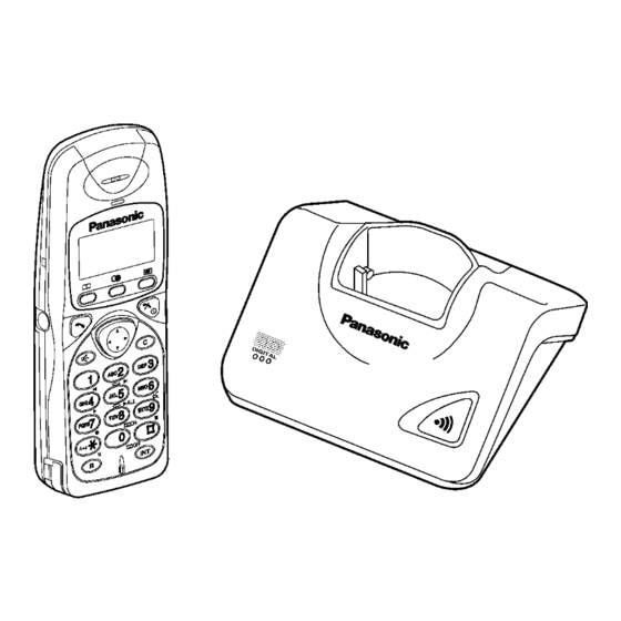
KX-TCD725AXM 1 LOCATION OF CONTROLS 1.1. Base Unit 1.2. Handset... -
Page 5: Displays
KX-TCD725AXM 2 Displays 2.1. Handset Display 2.2. Icons 2.3. Characters/Symbols... -
Page 6: Disassembly Instrucutions
KX-TCD725AXM 3 DISASSEMBLY INSTRUCUTIONS Shown in Fig.- To Remove Remove Lower Cabinet Screws (2.6 × 10)....(A) × 2 Main P.C.B of base Screw (2.6 × 10)....(B) × 1 Main P.C.B of base Charge wire solder Rear Cabinet of handset Screws (2 ×... -
Page 7: Assembly The Lcd To P.c. Board (Handset)
KX-TCD725AXM 3.1. Assembly the LCD to P.C. Board (Handset) -
Page 8: Settings
• • The telephone will not work during a power failure. We therefore recommend you use a standard telephone and automatic change-over switch to connect this Digital Cordless Phone to the line. Your Panasonic Sales Shop can offer you more... -
Page 9: Using The Belt Clip
KX-TCD725AXM 4.2. Using the Belt Clip You can hang the handset on your belt or pocket using the belt clip. 4.3. Batteries 4.3.1. Installing the Batteries in the Handset 4.3.2. Battery Charge 4.3.3. Recharge... - Page 10 KX-TCD725AXM 4.3.4. Battery Information...
-
Page 11: Operations
KX-TCD725AXM 5 OPERATIONS This section is intended to provide a basic overview for KX-TCD725AXM. For a full explanation, refer to the Operating Instructions. 5.1. Turning the Power ON/OFF 5.2. Making a Call 5.3. Answering Call 5.4. Terminating a Call... -
Page 12: Summary Of Programmable Function
KX-TCD725AXM 5.5. Summary of Programmable Function 5.5.1. Handset You can program the following function items using the handset near the base unit. Make sure that the power is ON, and the unit is in the standby mode. *1 See Setting a 4-digit Handset PIN (P.13) for more details. - Page 13 KX-TCD725AXM 5.5.1.1. Setting a 4-digit Handset PIN...
- Page 14 KX-TCD725AXM 5.5.2. Base Unit *1 If any key is not pressed over 60 seconds, the display will return to “Setting Base”. *2 See Setting a 4-digit Base Unit PIN (P.15) for more details.
- Page 15 KX-TCD725AXM 5.5.2.1. Setting a 4-digit Base Unit PIN...
-
Page 16: Registration
KX-TCD725AXM 5.6. Registration 5.6.1. Registering a Handset in the Base Unit... - Page 17 KX-TCD725AXM 5.6.2. Cancelling a Handset Registration in the Base Unit 5.6.3. Cancelling a Base Unit...
-
Page 18: Circuit Operation (Base Unit)
KX-TCD725AXM 6 CIRCUIT OPERATION (BASE UNIT) BLOCK DIAGRAM BASEBAND SECTION AND LINE INTERFACE (BASE UNIT) TXAF TXDA Burst Building 16kHz Bridge Hook Speech Encoding Audio RXAF RXDA Rect. Filter Switch Burst Decoding Speech Decoding Analog ADPCM RSSI Buzzer Front End... - Page 19 KX-TCD725AXM 6.1.3. FLASH PROM (SEE Fig. 18) The 2 Mbit (IC5) Flash PROM contains the operational firmware for the microcontroller. It is interfaced to the data/address/control bus using address lines A0 to A17, data lines D0 to D7, and chip select (pin 30), output enable (pin 32), and write (pin 7).
- Page 20 KX-TCD725AXM...
-
Page 21: The Line Interface Section
KX-TCD725AXM 6.2. THE LINE INTERFACE SECTION (SEE BLOCK DIAGRAM Fig. 17) 6.2.1. INTRODUCTION This section consists of the telephone line interface, bell detector, charge-pulse detector, CLIP detector hook switch, pulse dialing circuits, audio circuits, DC mask & line impedance circuits, power supplies, and battery charger circuits. - Page 22 KX-TCD725AXM 6.2.5. HOOKSWITCH (SEE Fig. 20) T8 is the hookswitch, driven by T9. When the phone is “off-hook”, the HOOK control signal from the BBIC will be a high logic level (+2.8V), and both transistors will be on, thus T8 will “loop” the line. The zenner diode D10 protects transistors T11 to T13 against transient line voltages.
- Page 23 KX-TCD725AXM 6.2.9. POWER SUPPLIES (SEE Fig. 21) The AC adaptor for the KX-TCD725 provides unregulated DC through J2 for the handset charge terminal, the 3.8V regulator (IC7) and the Relay coil (RL1) where fitted. The 3.8V supply from IC7 is used for the RF module, and is further reduced by IC1 to 2.80V for the BBIC supply.
-
Page 24: Rf Module
KX-TCD725AXM 6.3. RF MODULE BLOCK DIAGRAM RF MODULE ANT1 ANT2 PAON VCC1 Diversity 3.8V VCC2 Switching PAON PMB6610 voltage voltage regulator regulator PMB6818 DECT transceiver TXDA Power amp. VCC1 Printed balun Loop filter TX Part :N/A 32/33 DRON RXON SYRI Printed PLL &... -
Page 25: Circuit Operation (Handset)
KX-TCD725AXM 7 CIRCUIT OPERATION (HANDSET) BLOCK DIAGRAM BASEBAND SECTION (HANDSET) SPEAKER Amplifier SP_CTR Speaker RXDA EARPIECE RX-AF Speech Decoding Burst Decoding Buffer TXDA TX-AF Speech Encoding Burst Encoding Section HEADSET RSSI ADPCM Analog Codec SYRI Inter- Front Filter SYEN face... -
Page 26: The Base Band Section
KX-TCD725AXM 7.1. THE BASE BAND SECTION 7.1.1. INTRODUCTION The base-band section consists of a base-band integrated circuit (BBIC), a Flash PROM, an EEPROM, an LCD Display, a Microphone, an Earpiece, and power supply/battery management circuits. 7.1.2. THE BASE-BAND INTEGRATED CIRCUIT (BBIC) The PMB6723 (IC1) is a CMOS device designed to handle all the audio, signal and data processing needed in a DECT handset. - Page 27 KX-TCD725AXM 7.1.6. AUDIO PATH - TX AUDIO (SEE Fig. 25) The audio signal from the microphone (TP23) enters the BBIC at pin 44. RF decoupling and signal conditioning are provided by C17, R21, C14 and C25. In the BBIC the signal passes through the analogue section where it is amplified and converted to a digital audio stream signal.
- Page 28 KX-TCD725AXM Circuit Diagram...
- Page 29 KX-TCD725AXM 7.1.9. KEYBOARD (SEE Fig. 26) The keyboard “On” button is connected directly to pin 33 and 28 of the BBIC. When pressed it turns the handset on and off. All other keys are connected in a row/column matrix. They are scanned in five rows using scan pulses (only active when keys are pressed) from IC1 pins 15 to 19.
- Page 30 KX-TCD725AXM 7.1.11. BATTERY SUPPLY (SEE Fig. 27) A switch mode boost converter is used to provide a 3.8V supply from the battery. This supply is sensed by the BBIC through pin 26 (TP14) so that the switching rate can be controlled by a FET (T3) driven from pin 24 (TP13). A resistor on the Source of the FET provides a current sense at pin 25 (TP12).
-
Page 31: Rf Section
KX-TCD725AXM 7.2. RF SECTION DRON VCC1 3.8V VCC2 PAON PMB6610 voltage voltage regulator regulator PMB6818 DECT transceiver TXDA Power amp. VCC1 Printed balun Loop filter TX Part :N/A 32/33 PAON RXON SYRI PLL & Printed SYEN control logic SYDA SYCL... -
Page 32: Check Procedure (Base Unit)
KX-TCD725AXM 8 CHECK PROCEDURE (BASE UNIT) 8.1. PREPARATION 8.1.1. EQUIPMENT REQUIRED • • DECT tester: Romde & Schwarz, CMD 60 is recommended. • • Frequency counter: it must be precise to be able to measure 1Hz (precision;±4ppm). Hewlett Packard, 53131A is recommended. -
Page 33: Pc Setting
KX-TCD725AXM 8.3. PC SETTING 8.3.1. CONNECTIONS Note: See TELEPHONE LINE TESTS (P.35) for more details. 8.3.2. PC SETTING 1. Open a window of MS-DOS mode from the start-up menu. 2. Change a directory to the one with “RTX_COM” contained. 3. Type “SET RTX_COM=1” from the keyboard (when COM port 1 is used for the connection). -
Page 34: Set The Clock Frequency
KX-TCD725AXM 8.4. SET THE CLOCK FREQUENCY 1. Turn on the 9V supply (AC adaptor). 2. Enter "DEACTMAC" from the PC to switch off the RF unit. 3. Enter "CONTTX 0" to start continuous RF transmission. 4. Enter "RDEEPROM 00 00 0F" to display the first 15 hexadecimal bytes of the EEPROM. -
Page 35: Telephone Line Tests
KX-TCD725AXM 8.6. TELEPHONE LINE TESTS 1. Switch on the 9V power supply. 2. Connect a telephone cord from the base unit to the line/DTMF test set. 3. Enter "HOOKOFF" from the PC to invoke an off-hook condition. 4. Set the current limit to 40mA on the line simulator. -
Page 36: Base Unit Reference Drawing
KX-TCD725AXM 8.7. BASE UNIT REFERENCE DRAWING When connecting the Simulator and the Equipments to the P.C.B. for checking, refer to the illustrations below. -
Page 37: Check Procedure (Handset)
KX-TCD725AXM 9 CHECK PROCEDURE (HANDSET) 9.1. PREPARATION 9.1.1. EQUIPMENT REQUIRED • • DECT tester: Romde & Schwarz, CMD 60 is recommended. • • Frequency counter: it must be precise to be able to measure 1Hz (precision;±4ppm). Hewlett Packard, 53131A is recommended. -
Page 38: Pc Setting
KX-TCD725AXM 9.3. PC SETTING 9.3.1. CONNECTIONS 9.3.2. PC SETTING 1. Open a window of MS-DOS mode from the start-up menu. 2. Change a directory to the one with “RTX_COM” contained. 3. Type “SET RTX_COM=1” from the keyboard (when COM port 1 is used for the connection). -
Page 39: Set Clock Frequency
KX-TCD725AXM 9.4. SET CLOCK FREQUENCY 1. Turn on the 2.4V supply. 2. Switch the handset on at the keypad. 3. Enter "DEACTMAC" from the PC to switch off the RF unit. 4. Enter "CONTTX 0" to start continuous RF transmission. -
Page 40: Handset Reference Drawing
KX-TCD725AXM 9.6. HANDSET REFERENCE DRAWING When connecting the Simulator and the Equipments to the P.C.B. for checking, refer to the illustration below. -
Page 41: Troubleshooting Guide
KX-TCD725AXM 10 TROUBLESHOOTING GUIDE 10.1. HANDSET: DOES NOT OPERATE... -
Page 42: Handset: Link
KX-TCD725AXM 10.2. HANDSET: LINK... - Page 43 KX-TCD725AXM...
-
Page 44: Handset: Does Not Link
KX-TCD725AXM 10.3. HANDSET: DOES NOT LINK... -
Page 45: Battery Does Not Charge
KX-TCD725AXM 10.4. BATTERY DOES NOT CHARGE 10.5. NO VOICE RECEPTION... -
Page 46: Voice Transmission
KX-TCD725AXM 10.6. NO VOICE TRANSMISSION... -
Page 47: Base Unit: Does Not Link
KX-TCD725AXM 10.7. BASE UNIT: DOES NOT LINK... -
Page 48: Base Unit : Caller Id Problems
KX-TCD725AXM 10.8. BASE UNIT : CALLER ID PROBLEMS 10.9. BASE UNIT: TAM VOICE PROMPT PROBLEMS Cross Reference HANDSET: LINK (P.42) HANDSET: DOES NOT LINK (P.44) NO VOICE RECEPTION (P.45) EEPROM LAYOUT (BASE UNIT) (P.56) Note: *1 After replacing the base P.C.B., you need to cancel the registration of handset(s) in the base unit and re-register it. -
Page 49: Cabinet And Electrical Parts Location (Base Unit)
KX-TCD725AXM 11 CABINET AND ELECTRICAL PARTS LOCATION (BASE UNIT) -
Page 50: Cabinet And Electrical Parts Location (Handset)
KX-TCD725AXM 12 CABINET AND ELECTRICAL PARTS LOCATION (HANDSET) -
Page 51: Accessories And Packing Materials
KX-TCD725AXM 13 ACCESSORIES AND PACKING MATERIALS... -
Page 52: Replacement Parts List
KX-TCD725AXM 14 REPLACEMENT PARTS LIST Notes: 14.1.2. MAIN P.C.BOARD PARTS 1. RTL (Retention Time Limited) Ref. Part No. Part Name & Description Remarks The marking (RTL) indicates that the Retention Time is limited for this item. PCB1 PQWP1D725BXH MAIN P.C.BOARD ASS´Y (RTL) -
Page 53: Handset
KX-TCD725AXM Ref. Part No. Part Name & Description Remarks Ref. Part No. Part Name & Description Remarks ERJ3GEYJ101 ECUV1H151JCV 150P ERJ3GEYJ560 PSCEV1CA101S 100P ERJ3GEYJ103 ECUV1H100DCV ERJ3GEYJ103 PSCEV1CA101S 100P ERJ3GEYJ103 ECUV1H151JCV 150P ERJ3GEYJ102 ECUV1C104KBV ERJ3GEYJ560 ECUV1H100DCV ERJ3GEYJ101 ECUV1A225KB ERJ3GEYJ101 PQCUV1C105KB ERJ3GEYJ102... - Page 54 KX-TCD725AXM Ref. Part No. Part Name & Description Remarks Ref. Part No. Part Name & Description Remarks PQJC10048Y BATTERY TERMINALS (C) (OTHERS) PQJT10168Z CHARGE TERMINAL (L) PQJT10152Y CHARGE PAD PQJT10169Z CHARGE TERMINAL (R) PQJT10152Y CHARGE PAD PQKF10497Z5 REAR CABIET PQJT10152Y...
-
Page 55: Accessories And Packing Materials
KX-TCD725AXM Ref. Part No. Part Name & Description Remarks Ref. Part No. Part Name & Description Remarks ECST1AD227 C414 PQCUV1H222JC 0.0022 ECUV1C683KBV 0.068 C415 ECUV1H100DCV ECUV1H030CCV C416 0805N472J500 0.0047 ECUV1H220JCV C417 ECUV1H103KBV 0.01 PQCUV1H333JC 0.033 C418 ECUV1H1R5CCV ECUV1H220JCV C419 ECUV1H100DCV... -
Page 56: Eeprom Layout (Base Unit)
KX-TCD725AXM 15 EEPROM LAYOUT (BASE UNIT) 15.1. Scope The purpose of this section is to describe the layout of the EEPROM (IC9) for the TCD725 Base Unit. The EEPROM contains hardware, software, and user specific parameters. Some parameters are set during production of the base e.g. - Page 57 KX-TCD725AXM 15.3.3. Free Block 1 Address Default Name Type Description RunTimeErrorLogConfig Reserved Not used yet 161-162 00..00 RunTimeErrorLogAddress Last RunTime error (unit16) 163-164 00..00 RunTimeErrorCounter Number of runtime errors since last default programming (unit16) 0165 - 01FF FF..FF FreeBlock1 Free Block 1 15.3.4.
- Page 58 KX-TCD725AXM 15.3.5. BsNalTask Address Default Name Type Description 0240 0x01 ARSCountryCorrespondance ARS Country Correspondance 0 = Negative matching: No area code match -> Carrier is inserted. 1 = Positive matching: Match on area code -> Carrier is inserted. 2 = French matching:...
- Page 59 KX-TCD725AXM Address Default Name Type Description 0F02 UserCfg.RPauseTime User configuration (MMI) - "R"-pause. If disabled, normal dial pause (DialPauseTime) is used. Bit 7..0 :"R" pause time, zero value allowed Unit : 50 ms, defaults to 800 ms. 0F03 UserCfg.DialPauseTime User configuration (MMI) - dial pause.
- Page 60 KX-TCD725AXM Address Default Name Type Description 0F14 AgcUpdateTime Line AGC update time. The period of time between each line AGC update. If FFh, line-AGC is disabled. If used recommended value is 64h (1 sec). Unit : 10ms, min/max: 10/FF, Defaults to disabled.
- Page 61 KX-TCD725AXM 15.3.8. TADTASK Address Default Name Type Description 0F40 0x00 CountryCode Country code 0: Germany 1: Greece 2: Turkey 3: England 4: Switzerland 5: Poland 7: France 8: Denmark A: Italy C: Czech E: Hungary F: Spain 14: Russia 0F41-60...
- Page 62 KX-TCD725AXM Address Default Name Type Description 0F6B-0FF7 Free block Free Block 15.3.9. BsUiTask Address Default Name Type Description 0FFB - 0FFC (TCD715 / Config BsUiTask configuration (TCD700 / Bits 1=enable 0=disable TCD705 / 0: FlashTime1Enabled. TCD725) 1: FlashTime2Enabled. 0xF7, 0x01 2: FlashTime3Enabled.
-
Page 63: Appendix
KX-TCD725AXM 15.4. Appendix 15.4.1. Gain for transmit and receive [dB] [dB] [dB] [dB] [dB] 00 00 16.06 31 15 5.92 BB 22 -2.72 39 20 -11.02 48 D7 -29.51 00 01 16.9 21 41 5.73 AB 92 -2.92 A9 24 -11.2... - Page 64 KX-TCD725AXM 15.4.2. Gain for tonegenerator [dB] [dB] [dB] [dB] [dB] 6.02 -6.09 -17.79 -26.58 -36.26 3.52 -6.16 -17.93 -28.16 -36.40 1.94 -6.30 -17.99 -29.08 -36.68 1.02 -6.58 -18.06 -29.58 -37.28 0.53 -7.18 -18.13 -29.84 -38.62 0.27 -8.52 -18.20 -29.97 -40.21 0.13...
- Page 65 KX-TCD725AXM 15.4.3. Amplification by Shift & Add coeffecients [dB] [dB] [dB] [dB] [dB] 6.02 -6.09 -17.79 -26.58 -36.26 3.52 -6.16 -17.93 -28.16 -36.40 1.94 -6.30 -17.99 -29.08 -36.68 1.02 -6.58 -18.06 -29.58 -37.28 0.53 -7.18 -18.13 -29.84 -38.62 0.27 -8.52 -18.20...
- Page 66 KX-TCD725AXM 15.4.4. Gain index values Index Index Gain DspRam (dec) (hex) (dB) 0x00 0xC8C1 0x01 0x48C1 0x02 0xB8C0 0x03 0x98A6 0x04 0x48B4 0x05 0x28B7 0x06 0xC8B1 0x07 0x9931 0x08 0xC915 0x09 0x9A0D 0x0a 0x3920 0x0b 0xB923 0x0c 0xB931 0x0d 0xA9CB...
- Page 67 KX-TCD725AXM 15.4.5. Speakerphone gain DspRam Index Attenuation 0x02DA 0/0x00 -21 dB 0x0333 1/0x01 -20 dB 0x0397 2/0x02 -19 dB 0x0407 3/0x03 -18 dB 0x0485 4/0x04 -17 dB 0x0512 5/0x05 -16 dB 0x05B0 6/0x06 -15 dB 0x0662 7/0x07 -14 dB 0x072A...
-
Page 68: Eeprom Layout (Handset)
KX-TCD725AXM 16 EEPROM LAYOUT (HANDSET) 16.1. Scope The purpose of this section is to describe the layout of the EEPROM (IC2) TCD725 handset. The EEPROM contains hardware, software, and user specific parameters. Some parameters are set during production of the handset e.g. - Page 69 KX-TCD725AXM Address Default Name Type Description 0175 ZAP_3 ZAP for registration 3 0176 STATUS_3 Status for registration 3 0177-0186 ?? .. ?? UAK_3 UAK for registration 3 0187-018F ?? .. ?? Reserved Protocol data 0190-0194 ?? .. ?? RFPI_4 RFPI for registration 4...
- Page 70 KX-TCD725AXM Address Default Name Type Description 2AE - 2B0 FF FF FF AvailableLanguages Bit 0: 0:Disable, 1:Enable Spanish Bit 1: 0:Disable, 1:Enable Norwegian Bit 2: 0:Disable, 1:Enable French Bit 3: 0:Disable, 1:Enable Italian Bit 4: 0:Disable, 1:Enable Danish Bit 5: 0:Disable, 1:Enable Dutch...
- Page 71 KX-TCD725AXM 16.3.5. MMI Bits Address Default Name Type Description 1F00 EEToneConfig bit 0 - Keytone on/off - 1/0 bit 1 - Call waiting on/off - 1/0 bit 2 - Range alarm on/off - 1/0 bit 3 - Battery low alarm on/off - 1/0...
-
Page 72: Schematic Diagram (Base Unit)
KX-TCD725AXM 17 SCHEMATIC DIAGRAM (BASE UNIT) 17.1. Main +48V DC ON-HOOK +6.8V DC OFF-HOOK LINE VOLTAGE 48V DC +100mVrms at 1kHz (at 40mA) N.M. N.M. 48V DC CLIP (CALLER ID 1.4V DC IC10 +2.8V PULLS TOWARDS N.M. N.M. 0V DURING RING 3.8V DC... - Page 73 KX-TCD725AXM 0V DC ON-HOOK 0V DC ON-HOOK +6.7V DC OFF-HOOK +3.6V DC OFF-HOOK N.M. RX-AF TX-AF 220K 0V DC ON-HOOK +2.8V DC OFF-HOOK FREQUENCY: 96kHz 2.8V 10.368MHz burst +2.0V peak RX-DATA TX-DATA KX-TCD725AXM: SCHEMATIC DIAGRAM (BASE UNIT) Main...
-
Page 74: Rf Module
KX-TCD725AXM 17.2. RF Module IC402... - Page 75 KX-TCD725AXM IC402 IC400 KX-TCD725AXM: SCHEMATIC DIAGRAM (BASE UNIT) RF Module...
-
Page 76: Schematic Diagram (Handset)
KX-TCD725AXM 18 SCHEMATIC DIAGRAM (HANDSET) 18.1. Main Frequency 160kHz 4.1V 3.8V DC 2.4V 2.65V DC 3.4V to 4.8V SWITCHING DURING CHARGE 7.2V 2.2V LED ON 0V LED OFF 2.65V... - Page 77 KX-TCD725AXM 3.8V DC Frequency 10.368MHz RX-AF TX-AF 1.8V DC IN TALK MODE To RF SECTION 2.65V RX-DATA TX-DATA 10.368MHz burst 2.65V s typically 0.8V KX-TCD725AXM: SCHEMATIC DIAGRAM (HANDSET) Main...
-
Page 78: Rf Section
KX-TCD725AXM 18.2. RF Section IC402... - Page 79 KX-TCD725AXM IC402 IC400 KX-TCD725AXM: SCHEMATIC DIAGRAM (HANDSET) RF Section...
-
Page 80: Memo
KX-TCD725AXM 18.3. Memo... - Page 81 KX-TCD725AXM H.M. KXTCD725AXM...
-
Page 82: Circuit Board (Base Unit)
RF (IC4) Off-hook pin12 Voltage TP50 TP97 TP186 RF (IC4) pin44 TP65 TP82 TP110 TP66 RF UNIT TP101 IC11 TP98 C109 SYRI TP101 TP104 C102 R134 clock signal TP103 C105 C112 C101 C100 KX-TCD725AXM : BASE UNIT Main (Component View) -
Page 83: Flow Solder Side View
KX-TCD725AXM 19.2. Flow Solder Side View J2 pin1 J2 pin2 J100 Mode sel 2.8V KX-TCD725AXM : BASE UNIT Main (Flow Solder Side View) -
Page 84: Circuit Board (Handset)
KX-TCD725AXM 20 CIRCUIT BOARD (HANDSET) 20.1. Component View J1, +2.4V TP11 T6 collector TP24 supply 10.368MHz clock 2.65V IC400 J2, 0V DOWN LOAD KX-TCD725AXM : HANDSET Main (Component View) supply... -
Page 85: Flow Solder Side View
KX-TCD725AXM 20.2. Flow Solder Side View KX-TCD725AXM : HANDSET Main (Flow Solder Side View)