Table of Contents
Advertisement
Quick Links
DVD-Video Player
©
Copyright 2002 Philips Consumer Electronics B.V. Eindhoven, The Netherlands.
All rights reserved. No part of this publication may be reproduced, stored in a
retrieval system or transmitted, in any form or by any means, electronic,
mechanical, photocopying, or otherwise without the prior permission of Philips.
Published by PF0261 Service Singapore
Contents
1
2
3
4
5
6
7
Laser Supply - DVDalas2
8
9
10 Spare Part List
Printed in the Netherlands
Page
2
4
5
5
9
20
29
Diagr.
(Diagram M1) 30
37-42
(Diagram M2) 31
37-42
(Diagram M3) 32
37-42
(Diagram M4) 33
37-42
(Diagram M5) 34
37-42
(Diagram M6) 35
37-42
(Diagram M7) 36
37-42
43
45
45
56
Subject to modification
DVD Module SD-4
CL 16532163-013.eps
170102
EN 3122 785 12230
Advertisement
Table of Contents

Related Manuals for Philips SD-4


Summary of Contents for Philips SD-4
-
Page 1: Table Of Contents
All rights reserved. No part of this publication may be reproduced, stored in a retrieval system or transmitted, in any form or by any means, electronic, mechanical, photocopying, or otherwise without the prior permission of Philips. Published by PF0261 Service Singapore... -
Page 2: Technical Specifications
EN 2 SD-4 Technical Specifications 1. Technical Specifications Connections 12. YC5 13. GND 14. YC6 1.1.1 Connector 1701: Basic Connector 15. GND 16. YC7 1. I2CSCL/SIOCLK 17. GND 2. I2CSDA/SIODATA 18. HSYNC 3. SCART1 19. GND 4. SCART0 20. VSYNC 5. - Page 3 1.3.2 I2S Output Accuracy : Up to 24bit. Sample rate : 32kHz / 44.1kHz / 48kHz / 64kHz / 88.2kHz / 96kHz / 128kHz / 176.4kHz / 192kHz. Standard : Philips I2S output...
-
Page 4: Safety Instructions, Warnings, And Notes
EN 4 SD-4 Safety Instructions, Warnings, and Notes 2. Safety Instructions, Warnings, and Notes Safety Instructions Warnings 2.1.1 General Safety 2.2.1 General Safety regulations require that during a repair: • All ICs and many other semiconductors are susceptible to electrostatic discharges (ESD, "). Careless handling •... -
Page 5: Directions For Use (Not Available)
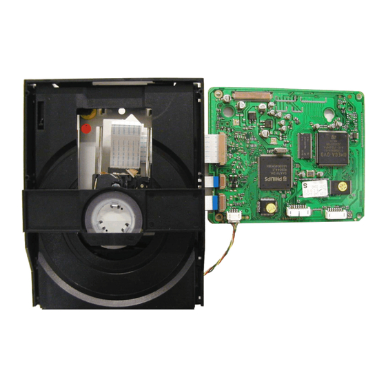
Directions for Use SD-4 EN 5 3. Directions for Use There is no DFU available 4. Mechanical Instructions The SD4.0 module can be configurate into 2 options as shown : Option 1 with monoboard below loader similar Option 2 with monoboard beside loader to allows for a lower total height of module CL 16532163_014.eps... - Page 6 EN 6 SD-4 Mechanical Instructions Dismantling Instruction CL 16532163_012.eps 030102 Figure 4-1...
- Page 7 Mechanical Instructions SD-4 EN 7 CL 16532163_015.eps 230102 Figure 4-2 CL 06532147_003.eps 4.1.1 Dismantling of DVD Mono Board 151100 Figure 4-4 See Figure 4-1 and 4-2 for dismantling of DVD module. It is possible to open the tray manually by moving the Slider in...
- Page 8 EN 8 SD-4 Mechanical Instructions Service Hints 4.2.1 DVD Module This module can be repaired as follows: 1. The VAL6013/01 is a combination of loading mechanism and DVD-mechanism. Both the mechanism is not a repairable unit and in case of failure it has to be replaced with a new loader VAL6013/01.
-
Page 9: Test Instructions Mono Board Dvd-Sd4.00
Test Instructions Mono Board DVD-SD4.00 SD-4 EN 9 5. Test Instructions Mono Board DVD-SD4.00 General PM3380B ch1: dT=73.0ms V1= 65.0mV • Impedance of measuring-equipment should be > 1MΩ. • Most tests have to be done by software commands. Together with the software command you will find a Ref.# nbr. - Page 10 EN 10 SD-4 Test Instructions Mono Board DVD-SD4.00 Ref. # Command Name Remark PM3380B PapChksFl Checksum FLASH CompSdramWrR SDRAM Write Read CompSdramWrR checks the complete SDRAM for failures inside the IC.The BasicInterconSDRAM check is done by writing & reading some well chosen patterns to all address and data interconnections of the SDRAM.
- Page 11 Test Instructions Mono Board DVD-SD4.00 SD-4 EN 11 Check the Mute output at testpoint T798: 0V ±0.3V PM3380B 5.4.5 Audio I2S Check To check the audio output, connect a audio DAC (on the A/V board) to the I2S output and start-up the audio test. Look at the audio outputs from the A/V board for both sine and pink noise.
- Page 12 EN 12 SD-4 Test Instructions Mono Board DVD-SD4.00 PM3380B PM3394B CH1 2.00 V~ MTB 100ns ch1+ CH1 2.00 V= BWL MTB100ns ch1+ CL06532065_009.eps CL 16532163_024.eps 161100 230102 Figure 5-8 PCMSCLK Figure 5-11 SPDIF To switch the audio signal OFF, press the STOP button on the PM3394B front.
- Page 13 Test Instructions Mono Board DVD-SD4.00 SD-4 EN 13 VIDEO PM3380B 5.5.1 Video Output Check Measure the DC voltages at all video-outputs at conn 1701 while the video signal is turned off: 1V ± 10% Generate a color-bar via next software commands: Ref.
- Page 14 EN 14 SD-4 Test Instructions Mono Board DVD-SD4.00 Check the level of SCART0 and SCART1 with the following commands: PM3380B Command Scart0 Scart1 Level on Pin 8 Ref. # Name (PIO3.6) (PIO3.7) of scart VideoScartLo 1 0-2V VideoScartMi 0 4.5-7V VideoScartHi 0 9.5-12V...
- Page 15 Test Instructions Mono Board DVD-SD4.00 SD-4 EN 15 5.5.3 Video Hsync Check. To measure the Video Hsync, the connector 1703 must be connected to the external video processing device such as high quality progressive scan codex and high quality Video DAC, else there will not be any waveform.
- Page 16 EN 16 SD-4 Test Instructions Mono Board DVD-SD4.00 5.6.2 Spindle Motor: PM3380B Before switching on the discmotor, check the following testpoints: Name Testpoint Value STDBY_MOTOR F308 MOTO1 F206 1V5 ±0.3 Switch the Discmotor ON/OFF with the following commands: Ref. # Command Name...
- Page 17 Test Instructions Mono Board DVD-SD4.00 SD-4 EN 17 5.6.3 Radial PM3380B Radial ON will only work when the PCB is connected to a CDM and DVD Disc is inserted. Switch the Radial control ON/OFF with the following commands: Ref. # Command Name...
- Page 18 EN 18 SD-4 Test Instructions Mono Board DVD-SD4.00 Name Testpoint Value Waveform PM3380B VOL - F327 10Vpp ±0.5V Refer to Figure 5-32 VOL + F326 10Vpp ±0.5V Refer to Figure 5-32 Measure input sledge control (sledge in HOME position) Name...
- Page 19 Test Instructions Mono Board DVD-SD4.00 SD-4 EN 19 Name Testpoint Value PM3394B F119 2.6V ±0.2% F127 2.6V ±0.2% F124 2.6V ±0.2% F122 2.6V ±0.2% F115 2.6V ±0.2% F117 2.6V ±0.2% At outputs of diodes A, B, C, D the following waveform can be...
-
Page 20: Diagnostic Software Description
EN 20 SD-4 Test Instructions Mono Board DVD-SD4.00 Diagnostic Software Description Logical Physical interface Interface Description components 5.7.1 Introduction Used for S2B Service PC, running a interface communication with S2B monitor program, the Basic Engine connected to the Purpose RS232 port of DVD... - Page 21 Test Instructions Mono Board DVD-SD4.00 SD-4 EN 21 menu will then appear. For the layout of the menus, see chapter “Layout of Menu and Submenu”. DVDv4 Diagnostic Software version 4.03 To switch between interfaces, the DVD player needs to be...
- Page 22 EN 22 SD-4 Test Instructions Mono Board DVD-SD4.00 5.9.3 S2B Interface LCD Display [30b] LCD BkLight [30c] Keyboard [27] Set-up Physical Interface Components LEDs [29] Hardware needed: Remote Control [28] • Control PC P50 Check [60] • one free COM port on the Control PC •...
- Page 23 Test Instructions Mono Board DVD-SD4.00 SD-4 EN 23 MAIN > BASIC ENGINE > S2B MENU Jump To Outside Grooves [42c S2B Echo [13] S2B Pass-Through [14] Screen Layout With Menus When menus are used, no specific screen layout can be given: MAIN >...
- Page 24 EN 24 SD-4 Test Instructions Mono Board DVD-SD4.00 5.11.3 Components 1. 0001 Unknown command ER @ 2. 3100 OK @ Ref. # Reference Name Remark 3. 0901 Data line X is not connected to the DRAM ER @ CompSdramWrR SDRAM Write Read 4.
- Page 25 Test Instructions Mono Board DVD-SD4.00 SD-4 EN 25 5.11.6 DisplayPWB (slave processor) 5.11.10 Karaoke Ref. # Reference Name Remark Ref. # Reference Name Remark DispVer Version number KaraokeModeOff Switch Karaoke mode off DispKeyb Keyboard KaraokeModeOn Switch Karaoke mode on DispRc...
- Page 26 EN 26 SD-4 Test Instructions Mono Board DVD-SD4.00 5.12.2 Basic Engine Nuclei Error code Error text 4242 “Unexpected response from Basic Engine” Error code Error text 4243 “Communication time-out error” 3900 Test successful 4244 “Basic Engine returned error number 0xXX”...
- Page 27 Test Instructions Mono Board DVD-SD4.00 SD-4 EN 27 Error Error code Error text code Error text 5820 Test successful 6001 “No readback on P50” 5840 Test successful 6002 “Disp not responding “ 5860 Test successful 6003 “P50 readback error” 5801 "Unexpected response from Basic Engine"...
- Page 28 EN 28 SD-4 Test Instructions Mono Board DVD-SD4.00 Error Error code Error text code Error text 3203 "Error log could not be read from NVRAM" 4720 “Total Power On time (minutes) : XX” 4721 The total power-on time could not be read from NVRAM.
-
Page 29: Block Diagram
Block Diagram SD-4 6. Block Diagram Block Diagram DIGITAL YUV SERVICE SERIAL 2S AUDIO OUTPUT INTERFACE OUTPUT CONN. 1501 CONN. 1703 CONN. 1700/2/5 SERVICE VSYNC PCMDATA1-3 HSYNC TXD_SER 27M_CLK RXD_SER RTS_SER CTS_SER 7605 7501 HFN,HFP OPTION RESET 74HCT14D 7600 SERVICE... -
Page 30: Electrical Diagrams & Pwb's
Electrical Diagrams and PWB’s SD-4 7. Electrical Diagrams and PWB’s Front-End Processor and Laser Supply - DVDalas2 1100 D1 F127 F2 2100 A10 F128 D11 2101 B9 F129 D11 2102 B2 F130 F2 2103 B5 F131 E11 2104 B9 F132 F2... -
Page 31: Front-End Processor Iguana
Electrical Diagrams and PWB’s SD-4 Front-End Processor Iguana 1200 A2 3282 H3 T218 E14 1210 D1 5200 B2 T219 E13 5201 C2 2200 A7 T220 E14 2201 B7 5202 F1 T221 E13 2202 B3 5203 E11 T222 E14 5204 E11... -
Page 32: Front-End Loader Interface
Electrical Diagrams and PWB’s SD-4 Front-End Loader Interface 1300 D1 1301 A1 1303 H1 2300 A8 2301 C3 2302 B10 Front-end Loader Interface +5VDF 2303 C11 2304 C10 2305 E7 2300 2306 E7 2308 H9 7301 100n F325 2309 H12... -
Page 33: Back-End Memory
Electrical Diagrams and PWB’s SD-4 Back-End Memory 2401 B7 2402 B4 2410 B10 2411 B12 2412 C10 2413 C12 Back end - MEMORY 2414 C10 2415 C12 2416 C12 2417 H14 3402 F1 3420 C12 3425 G13 3426 G13 3427 F8... - Page 34 Electrical Diagrams and PWB’s SD-4 Back-End SDRAM and Service Interface 1501 E6 2502 B2 2503 B3 2508 B2 2509 B3 2514 C2 Back-end SDRAM and SERVICE INTERFACE 2515 C3 2520 C2 2521 D9 2522 D7 2523 F8 3500 C1 3521 B9...
-
Page 35: Back-End Sdram And Service Interface
Electrical Diagrams and PWB’s SD-4 Back-End Host Processor 1600 C10 F637 C8 2603 B3 F641 G14 2604 B4 F642 G14 2605 B9 F643 G14 2606 C12 F644 G14 2607 C12 F645 G14 2608 C13 F646 G14 Back end 2609 C13... -
Page 36: Back-End Module Interface
Electrical Diagrams and PWB’s SD-4 Back-End Module Interface C58 H5 3753 I9 F736 F10 C59 H5 3755 D8 F737 F12 C60 H5 3756 D9 F738 F8 C61 H5 3757 D9 F739 F9 C63 H5 3758 D9 F740 A9 1702 1700... - Page 37 Electrical Diagrams and PWB’s SD-4 Top View (Overview) 1100 A2 2720 A3 3309 A1 3788 D3 PART 1 1210 B2 2721 A3 3310 A1 3789 D3 1300 A2 2722 A3 3311 A1 3790 D3 CL 16532163_08a.eps 1301 A1 2724 B3...
- Page 38 Electrical Diagrams and PWB’s SD-4 Detailed Top View Part 1 PART 1 CL 16532163_08a.eps 030102...
- Page 39 Electrical Diagrams and PWB’s SD-4 Detailed Top View Part 2 PART 2 CL 16532163_08b.eps 030102...
- Page 40 Electrical Diagrams and PWB’s SD-4 Bottom View (Overview) 2102 A2 2625 C1 3232 B2 3703 B1 7104 A2 PART 1 2103 A2 2626 C2 3233 B2 3704 B1 7201 B2 2106 A2 2627 C2 3234 B2 3706 B1 7202 B2 CL 16532163_09a.eps...
- Page 41 Electrical Diagrams and PWB’s SD-4 Detailed Bottom View Part 1 PART 1 CL 16532163_09a.eps 030102...
- Page 42 Electrical Diagrams and PWB’s SD-4 Detailed Bottom View Part 2 PART 2 CL 16532163_09b.eps 030102...
-
Page 43: Testpoint Overview
Electrical Diagrams and PWB’s SD-4 Testpoint Overview F100 B1 F171 A2 F271 A1 F503 D3 F708 A1 F787 A1 F101 B2 F172 B2 F272 B2 F504 D3 F709 A1 F788 A1 F102 B2 F173 B2 F273 B3 F505 C3 F710 A1... - Page 44 Electrical Diagrams and PWB’s SD-4 Personal notes: Personal notes:...
-
Page 45: Alignments (Not Available)
Features The SD4.0 modules consist of the Mercury 3 Loader Audio Video Others VAL6013/01 (from Philips Optical Storage), and a Mono Board. The module is capable of analogue video (with option for digital YUV video) and digital audio. Module interface CL 16532163_047.eps... - Page 46 EN 46 SD-4 Circuit Descriptions, List of Abbreviations and IC Data The Servo Processor/Decoder SAA7812 1Mbits of the memory is accessible. Conversely, when this pin The servo circuit in the SAA7812 (item 7200) takes care of the is HIGH, the upper 1Mbits is accessible.
- Page 47 Circuit Descriptions, List of Abbreviations and IC Data SD-4 EN 47 External Memory the other three channels (pins 32, 33 and 34) are Y, C, and The STi55xx family is capable of accessing external memory CVBS. via three buses: A new video output buffer (see diagram M7, e.g. item 7707 for •...
- Page 48 EN 48 SD-4 Circuit Descriptions, List of Abbreviations and IC Data New FTD 9.3.5 Top Side Connectors In the fourth DVD player generation (VFM2002), a new FTD is used, which requires a new serial bus (SIO instead of I2C bus).
-
Page 49: Pwb
Serial Clock I2C SCLK Audio serial bit clock Serial Data I2C SDRAM Synchronous DRAM S/PDIF Sony Philips Digital InterFace SRAM Static RAM STBY Standby SVCD Super Video CD Software Total Harmonic Distortion Transistor Transistor Logic (5V logic) -
Page 50: Diagram M1
EN 50 SD-4 Circuit Descriptions, List of Abbreviations and IC Data IC Data In this paragraph, the internal blockdiagrams and pinning are given of ICs that are drawn as 'black box' in the electrical diagrams (with exception of 'memory' and 'logic' ICs). - Page 51 Circuit Descriptions, List of Abbreviations and IC Data SD-4 EN 51 TZA1033 Pinning (item 7100) DVDALAS2plus Advanced Analogue DVD TZA1033 Signal Processor and Laser Supply PINNING handbook, full pagewidth CD-A CD-B CD-C CD-D CD-REF VDDA4 CD-E VSSA4 CD-F VDDA1 VSSA1...
-
Page 52: Diagram M2
EN 52 SD-4 Circuit Descriptions, List of Abbreviations and IC Data 9.5.2 Diagram M2 SAA7812HL Block Diagram (item 7200) Channel decoder Block decoder/ CD/DVD Erco encoder DRAM interface drive Host Bit Detector Memory Proc & Demodulator interface interface Memory Proc... - Page 53 Circuit Descriptions, List of Abbreviations and IC Data SD-4 EN 53 SAA7812HL Pinning (item 7200) DASP DAC_RP DA2_GRD DAC_RN DAC_VPOS PDIAG DAC_VNEG DA1_GWR DAC_LP IOCS16 DAC_LN INTRQ TEST1 DMACK_GRQ TEST2 IORDY CRIN DIOR CROUT DIOW DMARQ_GACK HFIN_DN SAA7812 M3x HFIN_DP...
-
Page 54: Diagram M6
EN 54 SD-4 Circuit Descriptions, List of Abbreviations and IC Data 9.5.3 Diagram M6 STi5580 Block Diagram (item 7600) 2 UART & Internal peripherals 2 SmartCards Central CACHE SUBSYSTEM command port (C2+) Front-end & link interface Clock DMAs ICache generator... - Page 55 Circuit Descriptions, List of Abbreviations and IC Data SD-4 EN 55 STi5580 Pinning (item 7600) PIO2[5] CPU_DATA[13] PIO2[6] CPU_DATA[12] PIO2[7] CPU_DATA[11] VDD3_3 CPU_DATA[10] CPU_DATA[9] PIO3[0] CPU_DATA[8] PIO3[1] PIO3[2] VDD2_5 PIO3[3] CPU_DATA[7] PIO3[4] CPU_DATA[6] PIO3[5] CPU_DATA[5] PIO3[6] CPU_DATA[4] PIO3[7] CPU_DATA[3] VDD2_5...
- Page 56 EN 56 SD-4 Spare Parts List 10. Spare Parts List SD4 EU 2301 4822 126 14305 100nF 10% 16V 0603 2736 4822 124 12095 100µF 20% 16V 2302 4822 126 14305 100nF 10% 16V 0603 2737 4822 126 14305 100nF 10% 16V 0603...
- Page 57 Spare Parts List SD-4 EN 57 3302 4822 117 12917 1Ω 5% 0.062W CASE0603 3723 4822 051 30689 68Ω 5% 0.063W 0603 RC21 5606 2422 549 45153 IND FXD SM EMI 100mH z 3304 4822 051 30682 6k8 5% 0.062W...