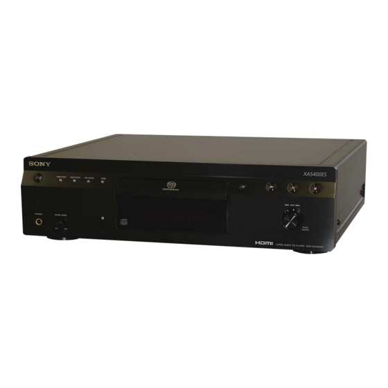
Sony SCD-XA5400ES Service Manual
Super audio cd player
Hide thumbs
Also See for SCD-XA5400ES:
- Operating instructions manual (36 pages) ,
- Specifications (8 pages) ,
- Limited warranty (1 page)
Table of Contents
Advertisement
SERVICE MANUAL
Ver. 1.0 2008.08
When a Super Audio CD is played
Playing frequency range
2 Hz to 100 kHz
Frequency response
2 Hz to 50 kHz (–3 dB)
Dynamic range
110 dB or more
Total harmonic distortion rate
0.0012 % or less
Wow and flutter
Value of measurable limit
(±0.001 % W. PEAK) or
less
When a CD is played
Frequency response
2 Hz to 20 kHz (±0.5 dB)
Dynamic range
100 dB or more
Total harmonic distortion rate
0.0017 % or less
Wow and flutter
Value of measurable limit
(±0.001 % W. PEAK) or
less
Sony Corporation
9-889-205-01
2008H05-1
Audio&Video Business Group
©
2008.08
Published by Sony Techno Create Corporation
SCD-XA5400ES
SPECIFICATIONS
Output jacks
Jack type Output
level
ANALOG
Phono
2 Vrms
OUT UN-
jacks
(at 50
BALANCED
kilohms)
ANALOG
XLR
2 Vrms
OUT
(at 50
BALANCED
kilohms)
HDMI
HDMI
DIGITAL
Square
–18 dBm
OUT (CD)
optical
OPTICAL*
output
connector
DIGITAL
Coaxial
0.5 Vp-p
OUT (CD)
output
COAXIAL*
connector
PHONES
Stereo
5 mW
phone jack
* Outputs only the audio signals of the CD
Canadian Model
Model Name Using Similar Mechanism
Mechanism Type
Optical Pick-up Block Name
General
Laser Diode Properties
Load
impedance
Over 10
kilohms
Over 600
ohms
(Light
emitting
Power requirements
wave
length: 660
nm)
75 ohms
Power consumption
Power consumption (during standby mode)
32 ohms
Dimensions (w/h/d)
Mass (approx.)
Supplied accessories
Audio connecting cord
Remote commander
AC power cord
Battery
Design and specifications are subject to change
without notice.
SUPER AUDIO CD PLAYER
US Model
AEP Model
NEW
CDM66F-DVBU101
KHM-313CAB
Emission duration:
Continuous
Laser Output*: Less than
44.6 μW
* This output is the value
measurement at a
distance of 200 mm from
the objective lens surface
on the Optical Pick-up
Block with 7 mm
aperture.
North America:
120 V AC, 60 Hz
Europe:
230 V AC, 50/60 Hz
25 W
0.5 W
430 × 124 × 390 mm
(17 × 5 × 15 3/8 inch) incl.
projecting parts
10.2 kg (22 lb 8 oz)
Red and White plugs (1)
RM-ASU042 (1)
(1)
R6 (size-AA) (2)
Advertisement
Table of Contents

Related Manuals for Sony SCD-XA5400ES


Summary of Contents for Sony SCD-XA5400ES
-
Page 1: Specifications
Red and White plugs (1) Remote commander RM-ASU042 (1) AC power cord Battery R6 (size-AA) (2) Design and specifications are subject to change without notice. SUPER AUDIO CD PLAYER Sony Corporation 9-889-205-01 2008H05-1 Audio&Video Business Group © 2008.08 Published by Sony Techno Create Corporation... - Page 2 LES DIAGRAMMES SCHÉMATIQUES ET LA LISTE DES PIÈCES SONT CRITIQUES POUR LA SÉCURITÉ DE FONC- TIONNEMENT. NE REMPLACER CES COMPOSANTS QUE PAR DES PIÈCES SONY DONT LES NUMÉROS SONT DON- Earth Ground NÉS DANS CE MANUEL OU DANS LES SUPPLÉMENTS Fig.
-
Page 3: Table Of Contents
SCD-XA5400ES TABLE OF CONTENTS SERVICING NOTES ..........GENERAL ..............DISASSEMBLY 3-1. Disassembly Flow ............3-2. Case ................. 3-3. Loading Panel Assy ............3-4. Front Panel Assy ............. 3-5. MAIN Board ..............10 3-6. Mechanism Deck (CDM66F-DVBU101) ....... 10 3-7. MOTOR Board, Motor (L) Assy (Loading) ....11 3-8. -
Page 4: Servicing Notes
SCD-XA5400ES SECTION 1 SERVICING NOTES Compatible Disc Types NOTES ON HANDLING THE OPTICAL PICK-UP BLOCK OR BASE UNIT You can play the following types of discs on this player. The laser diode in the optical pick-up block may suffer electrostat- •... - Page 5 SCD-XA5400ES HOW TO OPEN THE TRAY WHEN POWER SWITCH TURNS OFF – BOTTOM VIEW – cam (66) Pull out the tray in the direction of arrow Rotate the cam (66) with a tapering driver in the direction of arrow MAIN BOARD SERVICE POSITION In checking the MAIN board, prepare jig (extension cable J-2501-102-A: 1 mm Pitch, 13 cores, Length 300 mm).
-
Page 6: General
SCD-XA5400ES SECTION 2 This section is extracted GENERAL from instruction manual. Front Panel HDMI button/lamp (power) switch button and lamp Turns the power of the player on or off. Sets whether the audio signal is output from the Pauses playback. The lamp lights up during HDMI OUT jack or not. - Page 7 SCD-XA5400ES Remote Inserting batteries into the SA-CD/CD button remote Switches between the Super Audio CD layer and the CD layer of a hybrid disc. Insert two R6 (size-AA) batteries into the HDMI button battery compartment with the + and – correctly Sets whether the audio signal is output from the oriented to the markings.
-
Page 8: Disassembly
SCD-XA5400ES SECTION 3 DISASSEMBLY • This set can be disassembled in the order shown below. 3-1. DISASSEMBLY FLOW 3-2. CASE (Page 8) 3-5. MAIN BOARD 3-3. LOADING PANEL ASSY (Page 10) (Page 9) 3-6. MECHANISM DECK 3-4. FRONT PANEL ASSY... -
Page 9: Loading Panel Assy
SCD-XA5400ES 3-3. LOADING PANEL ASSY Pull out the tray in the direction of arrow loading panel assy two screws (BVTP2.6 (3CR)) – BOTTOM VIEW – cam (66) Rotate the cam (66) with a tapering driver in the direction of arrow 3-4. -
Page 10: Main Board
SCD-XA5400ES 3-5. MAIN BOARD connector (CN506, CN1201, CN1202) six screws × (BVTP3 wire (flat type) (24 core) MAIN board (CN1101) wire (flat type) (13 core) wire (flat type) (19 core) (CN1100) (CN502) wire (flat type) (13 core) (CN501) two screws ×... -
Page 11: Motor Board, Motor (L) Assy (Loading)
SCD-XA5400ES 3-7. MOTOR BOARD, MOTOR (L) ASSY (LOADING) belt (LD) gear (LD) two screws × (B2.6 connector (CN012) cushion two claws tray (66F) motor (L) assy (loading) Remove two solders. MOTOR board 3-8. BASE UNIT BLOCK – BOTTOM VIEW –... -
Page 12: Test Mode
SCD-XA5400ES SECTION 4 TEST MODE CDM TEST Note 1: According to the following procedures when you ship it Aging test mode of CDM. (Return it to the customer). Procedure: 1. SERVICE MODE of step 6 and 7 (DVD EEPROM clearness) 1. - Page 13 SCD-XA5400ES List of trouble log Note: “nnn” of toggle article number is a generation frequency of the error. Test key Toggle article Type Content (Remote commander) number It was not possible to communicate with MTK fi ve seconds more continu-...
- Page 14 SCD-XA5400ES DVD SERVICE MODE 3. Executing IOP Measurement In order to execute IOP measurement, the following standard pro- Note: DVD SERVICE MODE is a service mode of super audio cedures must be followed. Procedure: When the DVD service mode is operated, the following, remote 1.
- Page 15 SCD-XA5400ES 7. Press the [ RETURN] button on the remote commander to 52. Open kick spindle error return to previous menu. 60: Focus on error 8. Press the [0] button on the remote commander to return to the 61: Seek fail error top menu of Remocon Diagnosis Menu.
-
Page 16: Electrical Adjustment
SCD-XA5400ES SECTION 5 ELECTRICAL ADJUSTMENT To Execute the Initialize Setup Data When the base unit is replaced, perform the adjustment and the measurement as shown below in this order. Procedure: 1. Press the [MENU] button on the remote commander and then EXECUTING IOP MEASUREMENT (See page 14) press the [CLEAR] button on the remote commander. -
Page 17: Diagrams
SCD-XA5400ES SECTION 6 DIAGRAMS 6-1. BLOCK DIAGRAM - SA-CD/CD SERVO Section - R-ch is omitted due to same as L-ch. DVDRFIP • SIGNAL PATH : SA-CD PLAY VOA/A DVDA : CD PLAY (ANALOG) VOB/B DVDB VOC/C DVDC : CD PLAY (DIGITAL) -
Page 18: Block Diagram - Hdmi Section
SCD-XA5400ES 6-2. BLOCK DIAGRAM - HDMI Section - (Page 19) SD-RAM REAMP, SERVO DSP, HDMI TRANSMITTER IC1104 IC1101 (2/2) • SIGNAL PATH XTALI EEPROM : SA-CD PLAY IC1103 RD0 – RD15 DQ0 – DQ15 EEWP CN1701 HDMI OUT TX2P 1 TMDS DATA2+ RA0 –... -
Page 19: Block Diagram - Main Section
SCD-XA5400ES 6-3. BLOCK DIAGRAM - MAIN Section - PDT, BDTR, PBCK, PLRCK, SBCK (Page 17) PDATA J252 IOUTR+ BUFFER LOW-PASS FILTER IC253 BDTR IOUTR- IC255 SWITCHING DSDL IC206 R-CH DSDR PBCK PBCK PLRCK PLRCK RELAY DRIVE SBCK INVERTER Q252, 253... -
Page 20: Block Diagram - Panel, Power Supply Section
SCD-XA5400ES 6-4. BLOCK DIAGRAM - PANEL, POWER SUPPLY Section - FLUORESCENT INDICATOR TUBE DRIVER SYSTEM CONTROLLER IC501 (4/4) IC802 FL_O_OUT FL_CLK FL_STB +3.3V XRST RY+3.3V REGULATOR ND801 IC153 FLUORESCENT PT003 +12V INDICATOR TUBE MAIN POWER AMP+12V REGULATOR TRANSFORMER IC106 RECT GRID DRIVE D121 –... - Page 21 SCD-XA5400ES THIS NOTE IS COMMON FOR PRINTED WIRING BOARDS AND SCHEMATIC DIAGRAMS. • Circuit Boards Location (In addition to this, the necessary note is printed in each block.) For Printed Wiring Boards. For Schematic Diagrams. OUT-SW board Note: Note: • X : Parts extracted from the component side.
-
Page 22: Printed Wiring Board - Main Section (1/2)
SCD-XA5400ES 6-5. PRINTED WIRING BOARD - MAIN Section (1/2) - • See page 21 for Circuit Boards Location. • : Uses unleaded solder. (NC) MAIN BOARD (COMPONENT SIDE) CN504 CN1701 C1728 IC1707 HDMI OUT RB1106 RB1105 C1727 C1729 R1754 R1757... -
Page 23: Printed Wiring Boards - Main Section (2/2)
SCD-XA5400ES 6-6. PRINTED WIRING BOARDS - MAIN Section (2/2) - • See page 21 for Circuit Boards Location. • : Uses unleaded solder. J691 (US, CND) S502 IR REMOTE J1701 MDMI PRIORITY D692 S501 COAXIAL OPTICAL REMOTE MULTI MAIN BOARD... -
Page 24: Schematic Diagram - Main Section (1/4)
SCD-XA5400ES 6-7. SCHEMATIC DIAGRAM - MAIN Section (1/4) - (1/4) MAIN BOARD REG01 IOPMON REG02 R1225 100k MAIN BOARD R1223 100k FCS- (3/4) CL1213 FCS- MAIN (Page 26) FCS+ VREFO BOARD FCS+ TRK+ (3/4) R1221 C1211 R1226 R1232 R1234 C1233 C1209 RF+3.3V... -
Page 25: Schematic Diagram - Main Section (2/4)
SCD-XA5400ES 6-8. SCHEMATIC DIAGRAM - MAIN Section (2/4) - • See page 38 for waveforms. • See page 38 for IC Block Diagrams. • See page 41 for IC Pin Function Description. MAIN BOARD (2/4) CN506 R579 JL645 P_CONT1 JL646... -
Page 26: Schematic Diagram - Main Section (3/4)
SCD-XA5400ES 6-9. SCHEMATIC DIAGRAM - MAIN Section (3/4) - • See page 38 for IC Block Diagrams. • See page 41 for IC Pin Function Description. MAIN (Page 27) BOARD (4/4) MAIN BOARD (3/4) C1145 C1135 C1165 C2108 R2180 0.033... -
Page 27: Schematic Diagram - Main Section (4/4)
SCD-XA5400ES 6-10. SCHEMATIC DIAGRAM - MAIN Section (4/4) - • See page 38 for IC Block Diagrams. (4/4) MAIN BOARD STT_D/P MAIN DMUTE BOARD (2/4) STT_M/2 (Page 25) CN1110 JL1130 CL1161 R1126 PBCK R1125 JL1131 CL1162 PLRCK C1103 JL1132 CL1163... -
Page 28: Printed Wiring Board - Audio Section (1/2)
SCD-XA5400ES • Semiconductor 6-11. PRINTED WIRING BOARD - AUDIO Section (1/2) - • See page 21 for Circuit Boards Location. • : Uses unleaded solder. Location Ref. No. Location IC151 IC152 IC153 IC154 IC155 IC156 IC201 AUDIO BOARD IC202 (COMPONENT SIDE) -
Page 29: Printed Wiring Boards - Audio Section (2/2)
SCD-XA5400ES 6-12. PRINTED WIRING BOARDS - AUDIO Section (2/2) - • See page 21 for Circuit Boards Location. • : Uses unleaded solder. SCD-XA5400ES... -
Page 30: Schematic Diagram - Audio Section (1/2)
SCD-XA5400ES 6-13. SCHEMATIC DIAGRAM - AUDIO Section (1/2) - • See page 38 for waveforms. • See page 38 for IC Block Diagrams. AUDIO BOARD (1/2) R150 R152 CL152 R151 FB151 IC292 IC155 CL187 CL185 INVERTER D-FILP FLOP IC292 IC155... -
Page 31: Schematic Diagram - Audio Section (2/2)
SCD-XA5400ES 6-14. SCHEMATIC DIAGRAM - AUDIO Section (2/2) - • See page 38 for IC Block Diagrams. (2/2) AUDIO BOARD CL222 C228 R228 C229 R230 R202 R222 R223 C223 Q202 1500p 100V 1/3W DTA114EKA 12.1 CL212 1/3W 1/3W 1/3W 1/3W... -
Page 32: Printed Wiring Boards - Panel Section
SCD-XA5400ES • Semiconductor 6-15. PRINTED WIRING BOARDS - PANEL Section - • See page 21 for Circuit Boards Location. • : Uses unleaded solder. Location Ref. No. Location D801 A-10 D802 D803 DISPLAY BOARD IC801 B-10 CN804 CL894 IC802 CL917... -
Page 33: Schematic Diagram - Display Board
SCD-XA5400ES 6-16. SCHEMATIC DIAGRAM - DISPLAY Board - • See page 38 for waveforms. • See page 38 for IC Block Diagrams. DISPLAY BOARD CN805 FL_G FL6V KEY0 KEY-L BOARD LED_HDMI CN809 (Page 34) IC801 REMOTE CONTROL RECEIVER IC801 NJL24H400A... -
Page 34: Schematic Diagram - Key Section
SCD-XA5400ES 6-17. SCHEMATIC DIAGRAM - KEY Section - KEY-R BOARD Q804 DTC114EKA-T146 LED DRIVE Q803 LED BOARD DTC114EKA-T146 LED DRIVE JW852 D802 R817 SEL5521C-TP15 D803 SEL5821A-TP15 R816 JW851 CN806 C814 C815 JOG BOARD CL882 LED_PLAY JW853 CL883 C817 0.01 LED_PAUSE... -
Page 35: Schematic Diagram - Power Board
SCD-XA5400ES 6-18. SCHEMATIC DIAGRAM - POWER Board - • See page 38 for IC Block Diagrams. POWER BOARD R106 R105 R104 C110 C112 C101 0.01 D129 D101 R103 UDZSTE-1727B EC10DS2-TE12L5 3.3k CN103 D130 D103 (AEP) CL102 UDZS-TE17-5.1B EC10DS2-TE12L5 C113 Q101 FLAC4.3... -
Page 36: Schematic Diagram - Standby Board
SCD-XA5400ES 6-19. SCHEMATIC DIAGRAM - STANDBY Board - • See page 38 for IC Block Diagrams. ∗F001,002 (Page 35) CN002 STANDBY BOARD T800mAL 250V (US,CND) F001 ∗ T500mAL 250V (AEP) PT002 MAIN POWER POWER BOARD TRANSFORMER CN101 CN003 F002 ∗... -
Page 37: Printed Wiring Boards - Power Section
SCD-XA5400ES 6-20. PRINTED WIRING BOARDS - POWER Section - • See page 21 for Circuit Boards Location. • : Uses unleaded solder. POWER BOARD STANDBY BOARD CLP101 CLP51 CN001 D102 D104 D103 D101 D108 D106 D105 D107 CN102 JW51 CLP103... - Page 38 SCD-XA5400ES • Waveforms IC1901 TC74LVX4053FT (EL) – MAIN Board – – AUDIO Board – – DISPLAY Board – 15 14 IC501 (XOUT) IC152 IC802 (OSC1) 3.9 Vp-p 2.9 Vp-p 1.4 Vp-p 632 ns 200 μs 20 ns 1 V/DIV, 200 μs/DIV...
- Page 39 SCD-XA5400ES IC155 TC7W74FU IC156 HD74LV161ATELL RIPPLE ENABLE CARRY OUTPUT CLEAR LOAD ENABLE IC202 DSD1796DBR VCC2L AGND3L POWER SYSTEM SUPPLY CLOCK MANAGER DSDL 1 CURRENT IOUTL– DSDR 2 SEGMENT DBCK 3 IOUTL+ CONVERTER PLRCK 4 PDATA 5 AGND2 PBCK 6 VCC1...
-
Page 40: Display Board
SCD-XA5400ES – DISPLAY Board – IC802 ML9208-03MBZ03B 64 VDD 63 DA 8 BIT SHIFT 62 CP REGISTER 61 CS 60 RESET COMMAND PORT DECODER DRIVER CONTROL CIRCUIT DRIVER ADRAM 16W × 2B TIMING TIMING GENERATOR2 GENERATOR1 CGRAM DCRAM 248W × 35B 16W ×... - Page 41 SCD-XA5400ES • IC Pin Function Description MAIN BOARD IC501 R5F3640DDFAR (SYSTEM CONTROLLER) Pin No. Pin Name Description 1, 2 No Use Not used CEC_RX_IN CEC serial data input from the HDMI OUT connector SIRCS_IN SIRCS signal input from the remote control receiver...
- Page 42 SCD-XA5400ES Pin No. Pin Name Description 65 to 73 No Use Not used KEY_INT Wake up signal input terminal LED_LAT Serial data latch pulse signal output terminal Not used No Use Not used PLL_IC_I2C_SDA I2C Two-way data bus with the clock generator...
- Page 43 SCD-XA5400ES MAIN BOARD IC1101 CXD9927R (RF AMP, SERVO DSP, HDMI TRANSMITTER) Pin No. Pin Name Description RF offset cancellation capacitor connecting terminal RFGC RF AGC loop capacitor connecting Not used IREF Reference current input terminal AVDD3 Power supply terminal (+3.3V)
- Page 44 SCD-XA5400ES Pin No. Pin Name Description XROMCS Chip select signal output to the fl ash ROM Address signal output to the fl ash ROM Read enable signal output to the fl ash ROM 79, 80 HD0, HD1 Two-way data bus terminal with the fl ash ROM...
- Page 45 SCD-XA5400ES Pin No. Pin Name Description 165, 166 AVDD3 Power supply terminal (+3.3V) EXT_CAP Not used 168, 169 AGND3, AGND18 Ground terminal TXCN TMDS clock signal (negative) output to the HDMI OUT connector TXCP TMDS clock signal (positive) output to the HDMI OUT connector AVDD18 Power supply terminal (+1.8V)
- Page 46 SCD-XA5400ES Pin No. Pin Name Description ADACVDD1, 228, 229 Power supply terminal (+3.3V) ADACVDD2 Rt/DIR_DI Serial data input terminal Not used Lt/DIR_DO Serial data output terminal Not used ADACVSS1 Ground terminal ADACVDD1 Power supply terminal (+3.3V) SADCVDD18 Power supply terminal (+1.8V)
-
Page 47: Exploded Views
SCD-XA5400ES SECTION 7 EXPLODED VIEWS Note: • -XX and -X mean standardized parts, so • Abbreviation The components identifi ed by mark 9 con- they may have some difference from the CND : Canadian model tain confi dential information. original one. -
Page 48: Display Board Section
INDICATOR (FILTER) 3-873-313-01 PLATE, INDICATION A-1544-255-A DISPLAY BOARD, COMPLETE 4-250-532-01 KNOB (HP-VOL) 1-835-567-51 WIRE (FLAT TYPE) (19 CORE) 2-893-374-01 SPRING, RING J801 1-770-904-11 JACK (LARGE TYPE) (PHONES) 4-942-568-41 EMBLEM (NO.5), SONY RV801 1-227-185-11 RES, VAR, CARBON (PHONE LEVEL) 3-087-053-01 +BVTP2.6 (3CR) -
Page 49: Front Panel Section
SCD-XA5400ES 7-3. FRONT PANEL SECTION not supplied supplied supplied supplied Ref. No. Part No. Description Remark Ref. No. Part No. Description Remark 3-873-309-01 PANEL, FRONT (AEP) 4-246-567-01 BUTTON (PLAY) (N) 3-873-309-11 PANEL, FRONT (US, CND) 4-246-567-31 BUTTON (PLAY) (X) 4-250-643-01... -
Page 50: Main Board Section
SCD-XA5400ES 7-4. MAIN BOARD SECTION not supplied PT003 supplied PT002 not supplied not supplied AUDIO board section Ref. No. Part No. Description Remark Ref. No. Part No. Description Remark A-1544-253-A POWER BOARD, COMPLETE (US, CND) 9 155 A-1567-313-A MAIN BOARD, COMPLETE (for SERVICE) (AEP) -
Page 51: Audio Board Section
SCD-XA5400ES 7-5. AUDIO BOARD SECTION F001 not supplied F002 not supplied chassis section Ref. No. Part No. Description Remark Ref. No. Part No. Description Remark A-1544-254-A STANDBY BOARD, COMPLETE (US, CND) 4-860-518-00 CUSHION A-1544-320-A STANDBY BOARD, COMPLETE (AEP) 0 F001... -
Page 52: Chassis Section
SCD-XA5400ES 7-6. CHASSIS SECTION not supplied not supplied not supplied supplied not supplied not supplied supplied supplied supplied not supplied not supplied not supplied Ref. No. Part No. Description Remark Ref. No. Part No. Description Remark X-4955-348-1 FOOT ASSY 7-685-885-09... -
Page 53: Mechanism Deck Section (Cdm66F-Dvbu101)
SCD-XA5400ES 7-7. MECHANISM DECK SECTION (CDM66F-DVBU101) not supplied not supplied (OUT-SW board) not supplied M001 base unit section not supplied not supplied (MOTOR board) Ref. No. Part No. Description Remark Ref. No. Part No. Description Remark 3-452-881-01 TRAY (66F) 3-452-884-01... -
Page 54: Base Unit Section
SCD-XA5400ES 7-8. BASE UNIT SECTION Note: If wire (fl at type) is replaced, install it after bending it in the same form as that before replacement. Ref. No. Part No. Description Remark Ref. No. Part No. Description Remark 3-087-599-01 INSULATOR SCREW... -
Page 55: Electrical Parts List
SCD-XA5400ES SECTION 8 AUDIO ELECTRICAL PARTS LIST Note: • Due to standardization, replacements in • SEMICONDUCTORS The components identifi ed by mark 9 con- the parts list may be different from the In each case, u: μ, for example: tain confi dential information. - Page 56 SCD-XA5400ES AUDIO Ref. No. Part No. Description Remark Ref. No. Part No. Description Remark C273 1-136-480-11 FILM 0.0015uF 100V C274 1-137-350-11 FILM 0.015uF 100V < JACK > C275 1-136-480-11 FILM 0.0015uF 100V J201 1-818-094-11 JACK, PIN 1P (AUDIO OUT UNBALANCED L)
- Page 57 SCD-XA5400ES AUDIO DISPLAY Ref. No. Part No. Description Remark Ref. No. Part No. Description Remark RY291 1-755-485-11 RELAY R202 1-247-750-11 CARBON 1/2W R203 1-247-750-11 CARBON 1/2W < VIBRATOR > R204 1-247-749-11 CARBON 1/2W R205 1-247-750-11 CARBON 1/2W X151 1-767-286-11 VIBRATOR, CRYSTAL (22.5792MHz)
- Page 58 SCD-XA5400ES KEY-L KEY-R MAIN Ref. No. Part No. Description Remark Ref. No. Part No. Description Remark < CONNECTOR > < RESISTOR > CN801 1-779-978-11 PIN, CONNECTOR 3P R813 1-216-821-11 METAL CHIP 1/10W < JACK > R814 1-216-821-11 METAL CHIP 1/10W...
- Page 59 SCD-XA5400ES MAIN Ref. No. Part No. Description Remark Ref. No. Part No. Description Remark C593 1-104-658-91 ELECT 100uF C1169 1-107-826-11 CERAMIC CHIP 0.1uF C1170 1-162-965-11 CERAMIC CHIP 0.0015uF C594 1-104-658-91 ELECT 100uF C1171 1-107-826-11 CERAMIC CHIP 0.1uF C691 1-128-994-21 ELECT CHIP...
- Page 60 SCD-XA5400ES MAIN Ref. No. Part No. Description Remark Ref. No. Part No. Description Remark C2108 1-127-760-11 CERAMIC CHIP 4.7uF 6.3V C2109 1-126-916-11 ELECT 1000uF 6.3V < IC > C2110 1-126-916-11 ELECT 1000uF 6.3V C2114 1-107-826-11 CERAMIC CHIP 0.1uF IC501 A-1567-243-A...
- Page 61 SCD-XA5400ES MAIN Ref. No. Part No. Description Remark Ref. No. Part No. Description Remark R515 1-216-833-11 METAL CHIP 1/10W R596 1-218-871-11 METAL CHIP 0.5% 1/10W R516 1-216-833-11 METAL CHIP 1/10W R597 1-218-879-11 METAL CHIP 0.5% 1/10W R517 1-216-833-11 METAL CHIP...
- Page 62 SCD-XA5400ES MAIN Ref. No. Part No. Description Remark Ref. No. Part No. Description Remark R1151 1-216-833-11 METAL CHIP 1/10W R1753 1-216-864-11 SHORT CHIP R1152 1-216-864-11 SHORT CHIP R1754 1-216-864-11 SHORT CHIP R1153 1-216-864-11 SHORT CHIP R1757 1-216-864-11 SHORT CHIP R1154...
- Page 63 SCD-XA5400ES MAIN MOTOR OUT-SW POWER Ref. No. Part No. Description Remark Ref. No. Part No. Description Remark < DIODE > < SWITCH > D101 8-719-210-33 DIODE EC10DS2 S501 1-692-991-11 SWITCH, SLIDE (DIGITAL OUT(CD)) D102 8-719-210-33 DIODE EC10DS2 S502 1-692-991-11 SWITCH, SLIDE (HDMI PRIORITY)
- Page 64 SCD-XA5400ES STANDBY Ref. No. Part No. Description Remark Ref. No. Part No. Description Remark A-1544-254-A STANDBY BOARD, COMPLETE (US, CND) 1-249-439-11 CARBON 1/4W A-1544-320-A STANDBY BOARD, COMPLETE (AEP) 0 R60 1-249-389-91 CARBON 1/4W ************************ 1-249-415-11 CARBON 1/4W 7-685-646-79 SCREW +BVTP 3X8 TYPE2 IT-3 <...
- Page 65 SCD-XA5400ES MEMO...
-
Page 66: Revision History
SCDXA5400ES REVISION HISTORY Checking the version allows you to jump to the revised page. Also, clicking the version at the top of the revised page allows you to jump to the next revised page. Ver. Date Description of Revision 2008.08...