
Related Manuals for Motorola MCP750


Summary of Contents for Motorola MCP750
- Page 1 MCP750 CompactPCI Single Board Computer Installation and Use MCP750A/IH4 July 2000...
- Page 2 All rights reserved. Printed in the United States of America. Motorola and the Motorola symbol are registered trademarks of Motorola, Inc. PowerPC™ and PowerPC750™ are trademarks of IBM Corporation, and are used by Motorola, Inc. under license from IBM Corporation.
-
Page 3: Safety Summary
The safety precautions listed below represent warnings of certain dangers of which Motorola is aware. You, as the user of the product, should follow these warnings and all other safety precautions necessary for the safe operation of the equipment in your operating environment. -
Page 4: Emi Caution
Flammability All Motorola PWBs (printed wiring boards) are manufactured with a flammability rating of 94V-0 by UL-recognized manufacturers. EMI Caution This equipment generates, uses and can radiate electromagnetic energy. It may cause or be susceptible to electromagnetic interference (EMI) if not installed and used with adequate EMI protection. - Page 5 While reasonable efforts have been made to assure the accuracy of this document, Motorola, Inc. assumes no liability resulting from any omissions in this document, or from the use of the information obtained therein. Motorola reserves the right to revise this document and to make changes from time to time in the content hereof without obligation of Motorola to notify any person of such revision or changes.
- Page 6 If the documentation contained herein is supplied, directly or indirectly, to the U.S. Government, the following notice shall apply unless otherwise agreed to in writing by Motorola, Inc. Use, duplication, or disclosure by the Government is subject to restrictions as set forth in subparagraph (b)(3) of the Rights in Technical Data clause at DFARS 252.227-7013 (Nov.
-
Page 7: Table Of Contents
Equipment Required ....................1-3 Overview of Start-up Procedure ................1-4 Unpacking Instructions ....................1-5 Hardware Configuration ....................1-5 MCP750 Base Board Preparation ................1-6 Flash Bank Selection (J6) ...................1-6 TMCP700 Transition Module Preparation..............1-9 Serial Ports 1 and 2 ...................1-11 Configuration of Serial Ports 3 and 4 ...............1-11 Hardware Installation..................1-16... - Page 8 PCI Local Bus Memory Map ................2-4 CompactPCI Memory Map ................2-5 PCI Arbitration ....................2-5 Interrupt Handling ....................2-6 DMA Channels....................2-7 Sources of Reset ....................2-7 Endian Issues ...................... 2-8 Processor/Memory Domain ................ 2-8 Role of the Raven ASIC................2-9 PCI Domain....................
- Page 9 Compact FLASH Memory Card...............3-21 TMCP700 Transition Module................3-21 Serial Interface Modules................3-22 CHAPTER 4 Connector Pin Assignments MCP750 Connectors ....................4-1 Common Connectors ....................4-2 CompactPCI Connectors (J1/J2).................4-2 CompactPCI User I/O Connector (J3) ..............4-4 Local Bus Expansion Connector (J4) ..............4-6 User I/O Connector (J5)..................4-7 PCI Mezzanine Card Connectors (J11/J12/J13/J14)...........4-8...
- Page 10 ENV - Set Environment..................... 6-2 Configuring the PPCBug Parameters ..............6-3 APPENDIX A Specifications Specifications......................A-1 Cooling Requirements ....................A-2 EMC Compliance ..................... A-2 APPENDIX B Related Documentation Motorola Computer Group Documents ..............B-1 Manufacturers’ Documents ..................B-2 Related Specifications ....................B-6...
- Page 11 Figure 1-2. MCP750 Switches, Headers, Connectors, Fuses, LEDs ......1-8 Figure 1-3. TMCP700 Connector and Header Locations ........1-10 Figure 1-4. MCP750/TMCP700 Serial Ports 1 and 2 (DTE Only)......1-13 Figure 1-5. TMCP700 Serial Ports 3 and 4 DCE Configuration ......1-14 Figure 1-6. TMCP700 Serial Ports 3 and 4 DTE Configuration ......1-15 Figure 1-7.
- Page 12 Table 2-1. Processor Default View of the Memory Map ...........2-3 Table 2-2. PBC DMA Channel Assignments.............2-7 Table 2-3. Classes of Reset and Effectiveness ............2-8 Table 3-1. MCP750 Features ..................3-1 Table 3-2. Multiplexing Sequence of the MX Function ..........3-16 Table 3-3. Fuse Assignments ...................3-18 Table 3-4.
- Page 13 Table 5-7. PPCBug Diagnostic Commands For High Availability Systems ... 5-15 Table 5-8. Unsupported PPCBug Diagnostic Commands ........5-16 Table A-1. MCP750 Specifications ................. A-1 Table B-1. Motorola Computer Group Documents ..........B-1 Table B-2. Manufacturers’ Documents ..............B-2 Table B-3. Related Specifications ................B-6...
-
Page 14: About This Manual
This manual provides general product information; hardware preparation, installation, and operating instructions along with a functional description of the MCP750 series Single Board Computers (SBCs). Model numbers and descriptions of the MCP750 series are included in the following table. Model Number... -
Page 15: Summary Of Changes
Chapter 4, Connector Pin Assignments summarizes the pin assignments for the groups of interconnect signals for the MCP750 and the TMCP700. Chapter 5, PPCBug provides information on the PPCBug and its architecture. Additionally, it describes the monitor (interactive command portion of the firmware), and provides instructions on using the PPCBug debugger and the associated special commands. -
Page 16: Comments And Suggestions
MCP750. Comments and Suggestions Motorola welcomes and appreciates your comments on its documentation. We want to know what you think about our manuals and how we can make them better. Mail comments to: Motorola Computer Group Reader Comments DW164 2900 S. - Page 17 is used for names of variables to which you assign values. Italic is also used for comments in screen displays and examples, and to introduce new terms. courier is used for system output (for example, screen displays, reports), examples, and system prompts. <Enter>, <Return>...
-
Page 18: Introduction
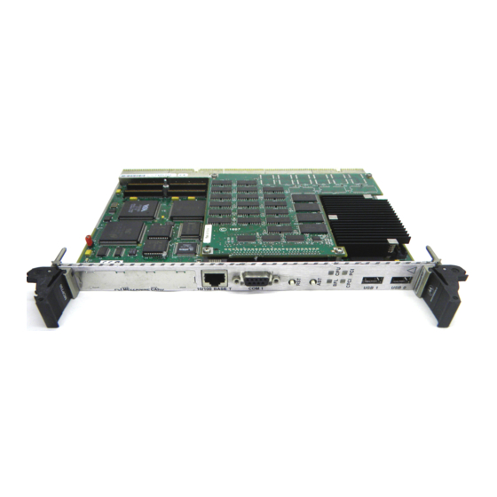
1Hardware Preparation and Installation Introduction The MCP750 is a single-slot Compact PCI board equipped with a PowerPC™ Series microprocessor. The board can be purchased with 32MB, 64MB, 128MB, or 256MB of ECC DRAM, is provided with 1m to 9m of linear FLASH memory, IDE Compact Flash memory, and 1MB of L2 cache memory (level 2 secondary cache memory). -
Page 19: Figure 1-1. Mcp750 Base Board Block Diagram
AT24C04 Ethernet PCI-PCI BRIDGE VT82C586B DEC21140 DEC21154 10BT/ Registers 100BTx NVRAM/ MK48T559 Super I/O PC87307 ESCC z8536 Z85230 Compact FLASH User I/O J3 & J5 ompactPCI J1/J2 Figure 1-1. MCP750 Base Board Block Diagram Computer Group Literature Center Web Site... -
Page 20: Equipment Required
Disk drives (and/or other I/O) and controllers Transition module (TMCP700) and connecting cables MCP750 modules are factory configured for I/O handling via a TMCP700 transition module. There are various MCP750 models available that correspond to different memory configurations. One transition module supports all configurations of the board. -
Page 21: Overview Of Start-Up Procedure
Refer also to the documentation provided with the equipment. Power up the system. Applying Power Note that the debugger initializes the MCP750 Using the Debugger You may also wish to obtain the PPCBug Firmware Package User’s Manual Initialize the system clock. -
Page 22: Unpacking Instructions
Caution Hardware Configuration To produce the desired configuration and ensure proper operation of the MCP750, you may need to carry out certain hardware modifications before installing the module. The MCP750 provides software control over most options: by setting bits in control registers after installing the module in a system, you can modify its configuration. -
Page 23: Mcp750 Base Board Preparation
MCP750 Base Board Preparation Figure 1-2 shows the location of switches, jumpers, connectors, and LED indicators on the MCP750. Manually configured items on the base board include: Flash bank selection (J6) For additional information on the configured items of the transition... - Page 24 MCP750 Base Board Preparation Flash Bank A Enabled Flash Bank B Enabled (1MB on base board) (4MB/8MB on RAM300 mezzanine) (Factory Configuration) http://www.motorola.com/computer/literature...
-
Page 25: Figure 1-2. Mcp750 Switches, Headers, Connectors, Fuses, Leds
Hardware Preparation and Installation Figure 1-2. MCP750 Switches, Headers, Connectors, Fuses, LEDs Computer Group Literature Center Web Site... -
Page 26: Tmcp700 Transition Module Preparation
TMCP700 Transition Module Preparation The TMCP700 transition module (refer to Figure 1-3) is used in conjunction with the MCP750 base board: The features of the TMCP700 include: A parallel printer port (IEEE 1284-I compliant) Two EIA-232-D asynchronous serial ports (identified as COM1 on the transition module’s panel) -
Page 27: Figure 1-3. Tmcp700 Connector And Header Locations
Hardware Preparation and Installation Figure 1-3. TMCP700 Connector and Header Locations 1-10 Computer Group Literature Center Web Site... -
Page 28: Serial Ports 1 And 2
X.21 (DCE and DTE) You can configure Serial Ports 3 and 4 for any of the above serial protocols by installing the appropriate serial interface module and setting the corresponding jumper. SIMs can be ordered separately as required. http://www.motorola.com/computer/literature 1-11... - Page 29 TMCP700 (listed in Appendix B, Related Documentation). The next three figures illustrate the MCP750 base board and TMCP700 transition module with the interconnections and jumper settings for DCE/DTE configuration on each serial port. 1-12...
-
Page 30: Figure 1-4. Mcp750/Tmcp700 Serial Ports 1 And 2 (Dte Only)
TMCP700 Transition Module Preparation MCP750 COM1 (Front Panel DB9) TMCP700 SOUT1 RTS1# DTR1# SIN1 CTS1# COM1 DSR1# DCD1# RI1# PC87307 SOUT2 RTS2# DTR2# SIN2 CTS2# COM2 DSR2# DCD2 RI2# 2098 9710 Figure 1-4. MCP750/TMCP700 Serial Ports 1 and 2 (DTE Only) http://www.motorola.com/computer/literature 1-13... -
Page 31: Figure 1-5. Tmcp700 Serial Ports 3 And 4 Dce Configuration
Hardware Preparation and Installation MCP750 TMCP700 Z85230 SCC EIA232-DTE SIM RTS# CTS# DCD# J8/J9 TRXC RTXC J3/MX Z8536 CIO DTR# LLB# RLB# DSR# 2097 9709 Figure 1-5. TMCP700 Serial Ports 3 and 4 DCE Configuration 1-14 Computer Group Literature Center Web Site... -
Page 32: Figure 1-6. Tmcp700 Serial Ports 3 And 4 Dte Configuration
TMCP700 Transition Module Preparation MCP750 TMCP700 Z85230 SCC EIA232-DTE SIM RTS# CTS# DCD# J8/J9 TRXC RTXC J3/MX Z8536 CIO DTR# LLB# RLB# DSR# 2096 9709 Figure 1-6. TMCP700 Serial Ports 3 and 4 DTE Configuration http://www.motorola.com/computer/literature 1-15... -
Page 33: Hardware Installation
MCP750 base board, the installation of the complete MCP750 assembly into a CompactPCI chassis, and the system considerations relevant to installation. Before installing the MCP750, ensure that the serial ports and all jumpers are properly configured. In most cases, the mezzanine card (RAM300 ECC DRAM module) is already in place on the base board. -
Page 34: Figure 1-7. Compact Flash Placement On Mcp750
AC cord or DC power lines from the system. Remove the chassis or system cover(s) as necessary to access the compact PCI module. 2117 9710 Figure 1-7. Compact FLASH Placement on MCP750 Inserting or removing modules with power applied may result in damage to module components. Caution To prevent injury, use extreme caution when handling, testing, and adjusting this equipment. -
Page 35: Ram300 Memory Mezzanine Installation
RAM300 mezzanine and into the standoffs on the MCP750. Tighten the screws. 8. Reinstall the MCP750 assembly in the proper card slot. Ensure that the module is properly seated in the backplane connectors. Do not damage or bend connector pins. -
Page 36: Figure 1-8. Ram300 Placement On Mcp750
AC cord or DC power lines from the system. Remove chassis or system cover(s) as necessary for access to the compact PCI module. 11661.00 9611 (2-3) Figure 1-8. RAM300 Placement on MCP750 Inserting or removing modules with power applied may result in damage to module components. Caution To prevent injury, use extreme caution when handling, testing, and adjusting this equipment. -
Page 37: Pmc Module Installation
RAM300 mezzanine and into the standoffs on the MCP750. Tighten the screws 6. Reinstall the MCP750 assembly in its proper card slot. Be sure the module is well seated in the backplane connectors. Do not damage or bend connector pins. -
Page 38: Figure 1-9. Pmc Module Placement On Mcp750
Dangerous voltages capable of causing death exist. Warning 3. Carefully remove the MCP750 from the CompactPCI card slot and place it on a clean and adequately protected working surface with connectors J1 and J5 facing you. Avoid touching areas of integrated circuitry; static discharge can damage these circuits. -
Page 39: Mcp750 Module Installation
(J11/12/13/14) on the MCP750. 6. Insert the four short phillips-head screws (provided with the PMC) through the holes on the bottom side of the MCP750 and the PMC front bezel and into rear standoffs. Tighten the screws. 7. Reinstall the MCP750 assembly in its proper card slot. Be sure the module is well seated in the backplane connectors. - Page 40 J3, J4, or J5 signals. 5. Slide the MCP750 into the system slot. Grasping the top and bottom injector handles, be sure the module is well seated in the P1 through P5 connectors on the backplane.
-
Page 41: Tmcp700 Transition Module Installation
TMCP700 Transition Module Installation The TMCP700 Transition Module may be required to complete the configuration of your particular MCP750 system. If so, perform the following steps to install this board. For additional information on the TMCP700 Transition Module refer, to the TMCP700 Transition Module Installation and Use manual (TMCP700A/IH). -
Page 42: Figure 1-10. Tmcp700/Mcp750 Mating Configuration
6. Replace the chassis or system cover(s), making sure no cables are pinched. Cable the peripherals to the panel connectors, reconnect the system to the AC or DC power source, and turn the equipment power on. MCP750 TMCP700 Figure 1-10. TMCP700/MCP750 Mating Configuration http://www.motorola.com/computer/literature 1-25... -
Page 43: System Considerations
Parity disabled (no parity) Baud rate of 9600 baud 9600 is the default baud rate for serial ports on MCP750 boards. After power-up you can reconfigure the baud rate if you wish, using the PPCBug PF (Port Format) command via the command line interface. Whatever the baud rate, some type of hardware handshaking —... - Page 44 MCP750 Module Power Requirements fuse assignments). The VIO, +12Vdc, and -12Vdc inputs are fused through polyswitches (resettable fuses). The +12Vdc and -12Vdc voltages are used only by the SIM modules on the TMCP700. All fused voltages are available on either J3, J4 or J5 for use on the transition module.
-
Page 45: Introduction
2Operating Instructions Introduction This chapter provides information applicable to the MCP750 family of Single Board Computers in a system configuration. This includes the power-up procedure along with descriptions of the switches and LEDs, memory maps, and software initialization. Applying Power... -
Page 46: Memory Maps
RUN SELFTESTS (IF ENABLED) AUTOBOOT (IF ENABLED) OPERATING SYSTEM 11734.00 9702 Figure 2-1. PPCBug System Startup The MCP750 front panel has switches and four LED ABORT RESET status indicators ( ). For additional information on front CPCI panel operation, refer to Chapter 3, Functional Description. -
Page 47: Processor Memory Map
The mapping of onboard resources as viewed by the CompactPCI The following sections provide a general description of the MCP750 memory organization from three points of view listed above. Detailed memory maps can be found in the MCP750 Series Single Board Computer Programmer’s Reference Guide (MCP750A/PG). Processor Memory Map The processor memory map configuration is under the control of the Raven bridge controller ASIC and the Falcon memory controller chip set. -
Page 48: Pci Local Bus Memory Map
If the rom_b_rv control bit is set, this address range maps to ROM/Flash bank B (socketed 1MB ROM/Flash). For detailed processor memory maps, including suggested PREP- compatible memory maps, refer to the MCP750 Series Single Board Computer Programmer’s Reference Guide (MCP750A/PG). PCI Local Bus Memory Map The PCI memory map is controlled by the Raven ASIC and by the 21154 PCI-to-PCI bridges. -
Page 49: Compactpci Memory Map
MCP750 Series Single Board Computer Programmer’s Reference Guide (MCP750A/PG). PCI Arbitration There are 6 potential local PCI bus masters on the MCP750 single-board computer: Raven ASIC (MPU/PCI bus bridge controller) DEC 21154 PCI-to-PCI bridge... -
Page 50: Interrupt Handling
The CPCI bus (interrupts from CPCI devices) Power monitor interrupts Watchdog timer interrupt The ISA bus (interrupts from ISA devices) For details on interrupt handling, refer to the MCP750 Series Single Board Computer Programmer’s Reference Guide (part number MCP750A/PG). Computer Group Literature Center Web Site... -
Page 51: Dma Channels
Channel 6 Serial Port 4 Transmitter (Z85230 Port B Tx) Channel 7 Not Used Sources of Reset The MCP750 SBC has five potential sources of reset: 1. Power-on/Undervoltage Reset. switch (will generate a hard reset when Front Panel RESET depressed). -
Page 52: Endian Issues
Operating Instructions The following table shows which devices are affected by the various types of resets. For details on using resets, refer to the MCP750 Series Single Board Computer Programmer’s Reference Guide (MCP750A/PG). Table 2-3. Classes of Reset and Effectiveness... -
Page 53: Role Of The Raven Asic
Since the Raven maintains address invariance in both little-endian and big- endian mode, no endian issues should arise for Ethernet data. Big-endian software must still take the byte-swapping effect into account when accessing the registers of the PCI/Ethernet device, however. http://www.motorola.com/computer/literature... -
Page 54: Introduction
This chapter describes the MCP750 single-board computer on a block diagram level. The General Description section provides an overview of the MCP750, followed by a detailed description of several blocks of circuitry. Figure 3-1 shows a block diagram of the board’s architecture. -
Page 55: General Description
Primary EIDE port routed to onboard Compact FLASH connector. Secondary EIDE port routed to the transition module General Description The MCP750 is a single-slot single-board computer equipped with an MPC750 PowerPC™ 750 Series microprocessor. The processor implements a backside cache controller and the board comes with 1MB of cache memory. - Page 56 NVRAM. The MCP750 interfaces to a CompactPCI bus using a DEC 21154 PCI-to- PCI bridge device. This device provides a 64-bit primary and a 64-bit secondary interface allowing full 64-bit data access between CompactPCI bus devices and the host/PCI bridge.
-
Page 57: Block Diagram
FLASH NVRAM Peripheral Bus ISA CSR Raven Controller Sys CSR SROM 32/64-Bit PCI Local Bus USB 1 USB 2 Expansion PCI-to-PCI Ethernet Connector Slot 1 Bridge 1 (Bridge 2) Figure 3-1. MCP750 Block Diagram Computer Group Literature Center Web Site... -
Page 58: Compactpci Interface
VIO pin for the primary and secondary bus buffers. The primary bus signalling voltage is tied to +5 volts. The secondary bus signalling voltage is tied to the CPCI bus VIO, so the MCP750 is a universal board that may operate in a +3.3V or +5V chassis. - Page 59 $08003E2xxxxx, where xxxxx is the unique 5-nibble number assigned to the board (that is, every board has a different value for xxxxx). Each MCP750 displays its Ethernet station address on a label attached to the base board in the PMC connector "keepout" area just behind the front panel.
-
Page 60: Pci Mezzanine Interface
(ATM), graphics, and Ethernet ports. The base board supports PMC front panel and rear transition module I/O. The MCP750 supports one PMC slot. Four 64-pin connectors on the base board (J11, J12, J13, and J14) interface with 32-bit or 64-bit IEEE P1386.1 PMC-compatible mezzanines to add any desirable function. -
Page 61: Asynchronous Serial Ports
ISASIO device. For additional programming information, refer to the PCI and ISA bus discussions in the MCP750 Programmer’s Reference Guide and to the vendor documentation for the ISASIO device. Floppy Disk/Tape Drive Controller The ISASIO device incorporates a PS/2-compatible low- and high-density disk drive controller for use with an optional external disk drive. -
Page 62: Keyboard And Mouse Interface
DIN connector on the transition module. Keyboard functions can be obtained by plugging the keyboard directly into this connector. To get both keyboard and mouse functions requires a Y adapter cable (Motorola Part Number: 30-W2309E01A). Refer to the TMCP700 Installation and Use manual for details. -
Page 63: Real-Time Clock/Nvram/Watchdog Timer Function
The clock generates no interrupts. Although the M48T559 is an 8-bit device, 8-, 16-, and 32-bit accesses from the ISA bus to the M48T559 are supported. Refer to the MCP750 Programmer’s Reference Guide (MCP750/PG) and to the M48T559 data sheet for detailed programming and battery life information. -
Page 64: Programmable Timers
Block Diagram Programmable Timers Among the resources available to the local processor are a number of programmable timers. Timers and counters on the MCP750 are provided by the Raven ASIC, the M48T559, the PBC, and the Z8536 CIO device (diagrammed in Figure 1-1). -
Page 65: M48T559 Watchdog Timer
The M48T559 contains one Watchdog timer. This Watchdog timer output is logically ORed with the Raven Watchdog timer 2 output to provide a hard reset. Refer to the device data sheet and the MCP750 Programmer’s Reference Guide (MCP750A/PG) for programming information. -
Page 66: Serial Communications Interface
Block Diagram Serial Communications Interface The MCP750 uses a Zilog Z85230 Enhanced Serial Communications Controller (ESCC) to implement the two serial communications interfaces, which are routed through the transition module. The Z85230 supports synchronous (SDLC/HDLC) and asynchronous protocols. The MCP750 hardware supports asynchronous serial baud rates of 110B/s to 38.4KB/s. -
Page 67: Base Module Feature Register
If cleared, there is on-board Ethernet support. Serial Port Signal Multiplexing Due to pin limitations of the J3 connector, the MCP750 multiplexes and de-multiplexes some signals between the MCP750 board and the TMCP700 transition module. This hardware function is transparent to the software. -
Page 68: Signal Multiplexing (Mx)
MXSYNC#, MXDO, and MXDI. MXCLK is the 10MHz bit clock for the time-multiplexed data lines MXDO and MXDI. MXSYNC# is asserted for one bit time at Time Slot 15 by the MCP750 board. MXSYNC# is used by the transition module to synchronize with the MCP750 board. MXDO is the time-multiplexed output line from the main board and MXDI is the time-multiplexed line from the transition module. -
Page 69: Table 3-2. Multiplexing Sequence Of The Mx Function
Functional Description Table 3-2. Multiplexing Sequence of the MX Function MXDO MXDI (From MCP750) (From TMCP700) TIME SLOT SIGNAL NAME TIME SLOT SIGNAL NAME RTS3 CTS3 DTR3 DSR3/MID1 LLB3/MODSEL DCD3 RLB3 TM3/MID0 RTS4 DTR4 CTS4 LLB4 DSR4/MID3 RLB4 DCD4 IDREQ... -
Page 70: Abort(Abt) Switch (S2)
The interrupt is normally used to abort program execution and return control to the debugger firmware located in the MCP750 and Flash memory. The interrupt signal reaches the processor module via ISA bus interrupt line IRQ8 . The signal is also available at pin PB7 of the Z8536 CIO device, which handles various status signals, serial I/O lines, and counters. -
Page 71: Fuses And Polyswitches (Resettable Fuses)
Ready) signal line on the CPCI bus is active. This indicates that the CPCI bus is active. Fuses and Polyswitches (Resettable Fuses) The MCP750 provides inline slow-blow fuses for each power rail including +5Vdc, +3.3Vdc, and PMC +5Vdc. Polyswitches are provided for VIO, keyboard/mouse Vcc, and the two USB output voltages, +12Vdc and -12Vdc. -
Page 72: Speaker Control
2 cache (L2 cache), and up to 9MB of Flash memory. The L2 cache and 1MB of 16-bit Flash memory reside on the MCP750 base board. The ECC DRAM and 4MB or 8MB of additional (64-bit) Flash memory are located on the RAM300 memory mezzanine. -
Page 73: Flash Memory
MPC750 microprocessor bus and the PCI local bus. Flash Memory The MCP750 base board has provision for 1MB of 16-bit Flash memory in two 8-bit sockets. The RAM300 memory mezzanine accommodates 4MB or 8MB of additional 64-bit Flash memory. -
Page 74: Compact Flash Memory Card
A or from bank B. Compact FLASH Memory Card The MCP750 supports a single EIDE compatible Compact FLASH Memory Card off of the PBC Primary EIDE interface. Currently available Compact FLASH memory cards provide from 2 Mbytes to 24 Mbytes of formatted capacity. -
Page 75: Serial Interface Modules
Functional Description A 34-pin header for a floppy port A 2-pin header for speaker output TMCP700 Transition Module Preparation on page 1-9 for more information. Serial Interface Modules The synchronous serial ports on the TMCP700 are configured via serial interface modules (SIMs), used in conjunction with the appropriate jumper settings on the transition module. -
Page 76: Mcp750 Connectors
4Connector Pin Assignments MCP750 Connectors This chapter summarizes the pin assignments for the following groups of interconnect signals for the MCP750 and the TMCP700: CompactPCI J1/J2 Connectors CompactPCI User I/O Connector J3 Local Bus Expansion Connector J4 User I/O Connector J5... -
Page 77: Common Connectors
CompactPCI Connectors (J1/J2) The MCP750 implements a 64-bit CompactPCI interface on connectors J1 and J2. J1 is a 110 pin AMP Z-pack 2mm hard metric type A connector with keying for +3.3V or +5V. J2 is 110 pin AMP Z-pack 2mm hard metric type B connector. -
Page 78: Table 4-2. J2 Compactpci Connector
No Connect No Connect No Connect No Connect (RSV) (RSV) (RSV) (RSV) (RSV) CLK6 No Connect No Connect No Connect (RSV) (RSV) (RSV) CLK5 No Connect No Connect (RSV) (RSV) No Connect No Connect No Connect (RSV) (RSV) (RSV) http://www.motorola.com/computer/literature... -
Page 79: Compactpci User I/O Connector (J3)
Connector Pin Assignments Table 4-2. J2 CompactPCI Connector (Continued) No Connect No Connect No Connect No Connect (BRSVP2A18) (BRSVP2B18) (BRSVP2C18) (BRSVP2E18) No Connect PRST_L REQ6_L GNT6_L (BRSVP2A17) No Connect No Connect DEG_L No Connect (BRSVP2A16) (BRSVP2B16) (BRSVP2E16) No Connect FAL_L REQ5_L GNT5_L (BRSVP2A15) -
Page 80: Table 4-3. J3 User I/O Connector
PMCIO30 PMCIO29 PMCIO28 PMCIO27 PMCIO26 PMCIO35 PMCIO34 PMCIO33 PMCIO32 PMCIO31 PMCIO40 PMCIO39 PMCIO38 PMCIO37 PMCIO36 PMCIO45 PMCIO44 PMCIO43 PMCIO42 PMCIO41 PMCIO50 PMCIO49 PMCIO48 PMCIO47 PMCIO46 PMCIO55 PMCIO54 PMCIO53 PMCIO52 PMCIO51 PMCIO60 PMCIO59 PMCIO58 PMCIO57 PMCIO56 PMCIO64 PMCIO63 PMCIO62 PMCIO61 http://www.motorola.com/computer/literature... -
Page 81: Local Bus Expansion Connector (J4)
Connector Pin Assignments Local Bus Expansion Connector (J4) Connector J4 is a 110 pin AMP Z-pack 2mm hard metric type A connector with keying for +3.3V or +5V. This connector routes the 64-bit local PCI bus to the backplane for expansion. The pin assignments for J4 are as follows (the outer row F is assigned and used as ground pins but is not shown in the table): Table 4-4. -
Page 82: User I/O Connector (J5)
SLIN_L SLCT BUSY ACK_L RTSa CTSa DTRa DCDa RXDa DSRa TXDa RTSb CTSb DTRb DCDb RXDb DSRb TXDb TR0_L WPROT_L RDATA_L HDSEL_L DSKCHG_L MTR1_L DIR_L STEP_L WDATA_L WGATE_L RESERVED INDEX_L MTR0_L DS1_L DS0_L CS1FX_L CS3FX_L DASP_L RESERVED IOCS16_L PDIAG_L http://www.motorola.com/computer/literature... -
Page 83: Pci Mezzanine Card Connectors (J11/J12/J13/J14)
RESET_L DRESET_L PCI Mezzanine Card Connectors (J11/J12/J13/J14) Four 64-pin connectors (J11/J12/J13/J14 on the MCP750) supply the interface between the base board and an optional PCI mezzanine card (PMC). The pin assignments are listed in the following two tables: Table 4-6. PCI Mezzanine Card Connector –12V... -
Page 84: Table 4-7. Pci Mezzanine Card Connector
PMCIO1 PMCIO2 C/BE7 PMCIO3 PMCIO4 C/BE6 C/BE5 PMCIO5 PMCIO6 C/BE4 PMCIO7 PMCIO8 +5V (Vio) PAR64 PMCIO9 PMCIO10 AD63 AD62 PMCIO11 PMCIO12 AD61 PMCIO13 PMCIO14 AD60 PMCIO15 PMCIO16 AD59 AD58 PMCIO17 PMCIO18 AD57 PMCIO19 PMCIO20 +5V (Vio) AD56 PMCIO21 PMCIO22 http://www.motorola.com/computer/literature... -
Page 85: Front Usb Connectors (J17/J18)
Not Used PMCIO63 PMCIO64 Front USB Connectors (J17/J18) Two USB Series A receptacles are located at the front panel of the MCP750 SBC. The pin assignments for these connectors are as follows: Table 4-8. USB 0 Connector J18 UVCC0 UDATA0N UDATA0P... -
Page 86: 10/100 Base-T Connector (J8)
UDATA1N UDATA1P 10/100 Base-T Connector (J8) The 10/100 Base-T Connector is an RJ45 connector located on the front panel of the MCP750 SBC. The pin assignments for this connector are as follows: Table 4-10. 10/100 Base-T Connector J8 AC Terminated... -
Page 87: Com1 Connector (J15)
Connector Pin Assignments COM1 Connector (J15) A standard DB9 receptacle is located on the front panel of the MCP750 to provide the interface to the COM1 serial port. These COM1 signals are also routed to J11 on the transition module. A terminal may be connected to J15 or J11 on the transition module but not both at the same time. - Page 88 PA21 PA22 PA23 PA24 PA25 PA26 PA27 PA28 PA29 PA30 PA31 PA_PAR0 PA_PAR1 PA_PAR2 PA_PAR3 RSRV PD10 PD11 PD12 PD13 PD14 PD15 PD16 PD17 PD18 PD19 PA20 PD21 PD22 PD23 PD24 PD25 PD26 PD27 PD28 PD29 PD30 PD31 http://www.motorola.com/computer/literature 4-13...
- Page 89 Connector Pin Assignments Table 4-12. Debug Connector (J19) (Continued) PD32 PD33 PD34 PD35 PD36 PD37 PD38 PD39 PD40 PD41 PD42 PD43 PD44 PD45 PD46 PD47 PD48 PD49 PA50 PD51 PD52 PD53 PD54 PD55 PD56 PD57 PD58 PD59 PD60 PD61 PD62 PD63 PDPAR0 PDPAR1...
- Page 90 Common Connectors Table 4-12. Debug Connector (J19) (Continued) SHARED DBWO AACK +3.3V ARTY XATS DRTY TBST No Connection No Connection No Connection No Connection No Connection TCLK_OUT MPUBG-0 No Connection MPUBR0 http://www.motorola.com/computer/literature 4-15...
- Page 91 Connector Pin Assignments Table 4-12. Debug Connector (J19) (Continued) MPUBR1 IRQ0 MPUBG1 MCHK WDT1TO WDT2TO CKSTPI L2BR CKSTPO L2BG HALTED (N/C) CLAIM TLBISYNC No Connection TBEN No Connection No Connection No Connection No Connection No Connection No Connection No Connection NAPRUN SRST1 QREQ...
-
Page 92: Dram Mezzanine Connector (J10)
Common Connectors DRAM Mezzanine Connector (J10) A 190-pin connector (J10 on the MCP750 base board) supplies the interface between the memory bus and the RAM300 DRAM mezzanine. The pin assignments are listed in the following table. Table 4-13. DRAM Mezzanine Connector (J10) - Page 93 Connector Pin Assignments Table 4-13. DRAM Mezzanine Connector (J10) (Continued) RDL6 RDL7 RDL8 RDL9 RDL10 RDL11 RDL12 RDL13 RDL14 RDL15 RDL16 RDL17 RDL18 RDL19 RDL20 RDL21 RDL22 RDL23 RDL24 RDL25 RDL26 RDL27 RDL28 RDL29 RDL30 RDL31 RDL32 RDL33 RDL34 RDL35 RDL36 RDL37 RDL38...
- Page 94 No Connection No Connection RDU0 RDU1 RDU2 RDU3 RDU4 RDU5 RDU6 RDU7 RDU8 RDU9 RDU10 RDU11 RDU12 RDU13 RDU14 +3.3V RDU15 RDU16 RDU17 RDU18 RDU19 RDU20 RDU21 RDU22 RDU23 RDU24 RDU25 RDU26 RDU27 RDU28 RDU29 RDU30 RDU31 RDU32 RDU33 http://www.motorola.com/computer/literature 4-19...
-
Page 95: Eide Compact Flash Connector (J9)
Connector Pin Assignments Table 4-13. DRAM Mezzanine Connector (J10) (Continued) RDU34 RDU35 RDU36 RDU37 RDU38 RDU39 RDU40 RDU41 RDU42 RDU43 RDU44 RDU45 RDU46 RDU47 RDU48 RDU49 RDU50 RDU51 RDU52 RDU53 RDU54 RDU55 RDU56 RDU57 RDU58 RDU59 RDU60 RDU61 RDU62 RDU63 CDU0 CDU1 CDU2... -
Page 96: Tmcp700 Transition Module
RST_L DIORDYA NO CONNECT NO CONNECT NO CONNECT NO CONNECT DATA8 DATA9 DATA10 TMCP700 Transition Module The following tables summarize the pin assignments of connectors that are specific to MCP750 modules configured for use with TMCP700 transition modules. http://www.motorola.com/computer/literature 4-21... -
Page 97: Compactpci Connectors (J3/J4/J5)
COM2 for COM1 are also routed to J15 on the MCP750. A terminal may be connected to J11 or J15 on the MCP750, but not both at the same time. The pin assignments are listed in the following table. Table 4-15. Serial Connections - Ports 1 and 2 (J10 and J11) (TMCP700 ) -
Page 98: Serial Ports 3 And 4 (J6/J24) (Tmcp700 I/O Mode)
Table 4-16. Serial Connections - Ports 3 and 4 (J6 and J24) (TMCP700) No Connection TXDn RXDn RTSn CTSn DSRn DCDn SPn_P9 SPn_P10 SPn_P11 SPn_P12 SPn_P13 SPn_P14 TXCIn SPn_P16 RXCIn LLBn SPn_P19 DTRn RLBn http://www.motorola.com/computer/literature 4-23... -
Page 99: Parallel Connector (J7) (Tmcp700 I/O Mode)
Connector Pin Assignments Table 4-16. Serial Connections - Ports 3 and 4 (J6 and J24) (TMCP700) (Continued) SPn_P23 TXCOn SPn-P26 Parallel Connector (J7) (TMCP700 I/O Mode) The parallel interface is implemented with an IEEE P1284 36-pin connector (J7) located on the TMCP700 transition module. The pin assignments are listed in the following table. -
Page 100: Keyboard/Mouse Connector (J16) (Tmcp700 I/O Mode)
The TMCP700 has two USB series A receptacles, J18, and J19. However, the standard version of the MCP700 board does not route the USB signals to these connectors in order to prevent long stubs on the MCP750 front panel USB connections. An alternate build option of the MCP750 may route the USB signals to the TMCP700 Transition Module in place of the MCP750 front panel connectors. -
Page 101: Eide Connector (J15)
Connector Pin Assignments EIDE Connector (J15) The TMCP700 provides a 40-pin header (J15) to interface to the MCP750 secondary EIDE port. The pin assignments and signal mnemonics for this connector are listed in the following table: Table 4-19. EIDE Connector (J15) -
Page 102: Floppy Port Connector (J17)
The TMCP700 has a 4-pin header that can be used to provide +5Vdc power to offboard devices. This power is derived from the fused +5Vdc power on the MCP750. Any external device powered from this connector must not draw more than 200mA. The pin assignments are listed in the following table. -
Page 103: Speaker Output Connector (J13)
+5Vdc No Connect Speaker Output Connector (J13) The 2-pin header (J13) provides connection to an external speaker from the MCP750 PCB Counter 2 output. The pin assignments are listed in the following table. Table 4-22. Speaker Output Connector (J13) Signal... - Page 104 TMCP700 Transition Module Table 4-23. PMC I/O Connector (J2) (Continued) Signal Signal PMCIO5 PMCIO6 PMCIO7 PMCIO8 PMCIO9 PMCIO10 PMCIO11 PMCIO12 PMCIO13 PMCIO14 PMCIO15 PMCIO16 PMCIO17 PMCIO18 PMCIO19 PMCIO20 PMCIO21 PMCIO22 PMCIO23 PMCIO24 PMCIO25 PMCIO26 PMCIO27 PMCIO28 PMCIO29 PMCIO30 PMCIO31 PMCIO32 http://www.motorola.com/computer/literature 4-29...
-
Page 105: Table 4-24. Pmc I/O Connector (J21)
Connector Pin Assignments Table 4-24. PMC I/O Connector (J21) Signal Signal PMCIO33 PMCIO34 PMCIO35 PMCIO36 PMCIO37 PMCIO38 PMCIO39 PMCIO40 PMCIO41 PMCIO42 PMCIO43 PMCIO44 PMCIO45 PMCIO46 PMCIO47 PMCIO48 PMCIO49 PMCIO50 PMCIO51 PMCIO52 PMCIO53 PMCIO54 PMCIO55 PMCIO56 PMCIO57 PMCIO58 PMCIO59 PMCIO60 4-30 Computer Group Literature Center Web Site... - Page 106 TMCP700 Transition Module Table 4-24. PMC I/O Connector (J21) (Continued) Signal Signal PMCIO61 PMCIO62 PMCIO63 PMCIO64 http://www.motorola.com/computer/literature 4-31...
-
Page 107: Chapter 5 Ppcbug
Documentation. PPCBug Basics The PowerPC debug firmware (PPCBug) is a powerful evaluation and debugging tool for systems built around the Motorola PowerPC microcomputers. Facilities are available for loading and executing user programs under complete operator control for system evaluation. The PPCBug provides a high degree of functionality, user friendliness, portability, and ease of maintenance. - Page 108 PPCBug Firmware Package User’s Manual, PPCBUGA1/UM and PPCBUGA2/UM). It is also referred to as “the debugger” or “PPCBug”. A command-driven diagnostics package for the MCP750 hardware, also referred to as the “diagnostics”. The diagnostics package is described in the PPCBug Diagnostics Manual (PPCDIAA/UM).
-
Page 109: Memory Requirements
MPU, Hardware, and Firmware Initialization The debugger performs the MPU, hardware, and firmware initialization process. This process occurs each time the MCP750 is reset or powered up. The steps below represent high-level outline (not all of the detailed steps are listed): 1. - Page 110 PPCBug 4. Clears all block address translation registers of the MPU. 5. Initializes the MPU-bus-to-PCI-bus bridge device. 6. Initializes the PCI-bus-to-ISA-bus bridge device. 7. Calculate the external bus clock speed of the MPU. 8. Delays for 750 milliseconds. 9. Determines the CPU board type. 10.
- Page 111 36. Extinguishes the board fail LED, if there are no self-test failures or initialization/configuration errors. 37. Executes the configured boot routine, either ROMboot, Autoboot, or Network Autoboot. 38. Executes the user interface (that is, displays the PPC1-Bug> prompt). PPC1-Diag> http://www.motorola.com/computer/literature...
-
Page 112: Using Ppcbug
PPCBug Using PPCBug PPCBug is command-driven; it performs its various operations in response to commands that you enter at the keyboard. When the prompt PPC1-Bug appears on the screen, the debugger is ready to accept debugger commands. When the prompt appears on the screen, the PPC1-Diag>... -
Page 113: Debugger Commands
HE, followed by a space, followed by the test category description (for example, UART), followed by a carriage return Table 5-1. Debugger Commands Command Description One Line Assembler Block of Memory Compare Block of Memory Fill Block of Memory Initialize Block of Memory Move Breakpoint Insert http://www.motorola.com/computer/literature... - Page 114 PPCBug Table 5-1. Debugger Commands (Continued) Command Description NOBR Breakpoint Delete Block of Memory Search Block of Memory Verify Concurrent Mode NOCM No Concurrent Mode CNFG Configure Board Information Block Checksum CSAR PCI Configuration Space READ Access CSAW PCI Configuration Space WRITE Access Data Conversion Block of Memory Move One Line Disassembler...
- Page 115 Memory Modify Memory Map Diagnostic Memory Set Memory Write Automatic Network Boot Nap MPU Network Boot Operating System, Halt Network Boot Operating System NIOC Network I/O Control NIOP Network I/O Physical NIOT Network I/O Teach (Configuration) NPING Network Ping http://www.motorola.com/computer/literature...
- Page 116 PPCBug Table 5-1. Debugger Commands (Continued) Command Description Offset Registers Display/Modify Printer Attach NOPA Printer Detach PBOOT Bootstrap Operating System Port Format NOPF Port Detach PFLASH Program FLASH Memory Put RTC into Power Save Mode ROMboot Enable NORB ROMboot Disable Register Display REMOTE Remote...
-
Page 117: High Availability Supported Commands
Although a command to allow the erasing and reprogramming of Flash memory is available to you, keep in mind that reprogramming any portion of the MCP750’s Flash memory (bank B) will erase everything currently Caution contained in the Flash memory, including the PPCBug debugger. -
Page 118: Unsupported Commands
PPCBug Unsupported Commands The following table lists standard PPCBug debugger commands that are not supported on the MCP750. Table 5-3. Unsupported Debugger Commands Name Description DMA Block of Memory Move FORK Fork Idle MPU at Address FORKWR Fork Idle MPU with Registers... -
Page 119: Unsupported System Call Interfaces
MPC750 hardware, including the High Availability (HA) features of the CPU module. It includes tests for: Memory Read/Write L2 Cache Real Time Clock Ethernet Controller ISA Bridge Serial Communications Controller UART Keyboard/Mouse Controller Parallel Interface PCI/PMC Interface EIDE http://www.motorola.com/computer/literature 5-13... -
Page 120: Diagnostic Tests
PPC1-Diag> displays, and all of the debugger and diagnostic commands are available. Note that not all tests are valid for the MCP750. Using the HE command, you can list the diagnostic routines available in each test group. Refer to the PPCBug Diagnostics Manual, listed in... -
Page 121: High Availability Specific Ppcbug Diagnostic Commands
3. Test Sets marked with an asterisk (*) are not available on the MCP750, unless SCSI or Video PMCs are installed. High Availability Specific PPCBug Diagnostic Commands The following table lists PPCBug diagnostic commands that have been added to support High Availability features. -
Page 122: Table 5-8. Unsupported Ppcbug Diagnostic Commands
PPCBug Table 5-8. Unsupported PPCBug Diagnostic Commands Name Description CL1283 Parallel Interface (Cirrus CL-CD1283) Tests CS4231 CS4231 Audio Codec Tests NCR 53C8XX SCSI I/O Processor Tests VGA543X VGA Controller (GD543X) Tests 5-16 Computer Group Literature Center Web Site... -
Page 123: Overview
Board Serial Number, the Board Identifier, the Bus Clock Speed, and other operational or ID characteristics. The example below displays a typical Board Information Block: Board (PWA) Serial Number = “2717994 ” Board Identifier = “MCP750-60X-0XX ” Artwork (PWA) Identifier = “01-w3378F01B ”... -
Page 124: Env - Set Environment
The data strings are padded with zeroes if the length is not met. It is important to note that the MCP750 has no local SCSI bus controller, hence, the Local SCSI Identifier parameter is ignored by the PPCBug. -
Page 125: Configuring The Ppcbug Parameters
Probe System for Supported I/O Controllers [Y/N] = Y? Accesses will be made to the appropriate system buses (for example, VMEbus, local MPU bus) to determine the presence of supported controllers (Default). Accesses will not be made to the VMEbus to determine the presence of supported controllers. http://www.motorola.com/computer/literature... - Page 126 Secondary SCSI Identifier = “07”? If the board has a secondary SCSI controller, this number is the secondary SCSI ID or address. For the MCP750, all PCI add-on SCSI controllers/adaptors supported by PPCBug are set to the SCSI ID value entered here.
- Page 127 Auto Boot Enable [Y/N] = N? The Autoboot function is enabled. The Autoboot function is disabled (Default). Auto Boot at power-up only [Y/N] = N? Autoboot is attempted at power-up reset only. Autoboot is attempted at any reset (Default). http://www.motorola.com/computer/literature...
- Page 128 CNFG and ENV Commands Auto Boot Scan Enable [Y/N] = Y? If Autoboot is enabled, the Autoboot process attempts to boot from devices specified in the scan list (for example, ) (Default). FDISK/CDROM/TAPE/HDISK If Autoboot is enabled, the Autoboot process uses the Controller LUN and Device LUN to boot.
- Page 129 Network Auto Boot Enable [Y/N] = N? The Network Auto Boot (NETboot) function is enabled. The NETboot function is disabled (Default). Network Auto Boot at power-up only [Y/N] = N? NETboot is attempted at power-up reset only. NETboot is attempted at any reset (Default). http://www.motorola.com/computer/literature...
- Page 130 CNFG and ENV Commands Network Auto Boot Controller LUN = 00? Refer to the PPCBug Firmware Package User’s Manual, listed in Appendix B, Related Documentation, for a listing of network controller modules currently supported by PPCBug (Default = $00). Network Auto Boot Device LUN = 00? Refer to the PPCBug Firmware Package User’s Manual for a listing of network controller modules currently supported by PPCBug (Default = $00).
- Page 131 Processor/Memory Mezzanine Module User’s Manual for appropriate values. The default value varies according to the system’s bus clock speed. Note ROM First Access Length is not applicable to the MCP750. The configured value is ignored by PPCBug. http://www.motorola.com/computer/literature...
- Page 132 The default value varies according to the system’s bus clock speed. Note ROM Next Access Length is not applicable to the MCP750. The configured value is ignored by PPCBug. DRAM Parity Enable [On-Detection/Always/Never - O/A/N] = 0? DRAM parity is enabled upon detection. (Default) DRAM parity is always enabled.
- Page 133 ENV - Set Environment this parameter, refer to the 8259 Interrupts section in Chapter 4 of the MCP750 Programmer’s Reference Guide, listed in Appendix B, Related Documentation. Serial Startup Code Master Enable [Y/N]=N? The Serial Startup Codes can be displayed at key points in the initialization of the hardware devices.
-
Page 134: Appendix A Specifications
Table A-1 lists the general specifications for MCP750 base boards. Subsequent sections detail cooling requirements and FCC compliance. A complete functional description of the MCP750 base boards appears in Chapter 3, Functional Description. Specifications for the optional PCI mezzanines can be found in the documentation for those modules. -
Page 135: Cooling Requirements
Specifications Cooling Requirements The Motorola MCP750 family of Single Board Computers is specified, designed, and tested to operate reliably with an incoming air temperature range from -5° to +55° C (32° to 131° F) with forced air cooling of the entire assembly (base board and modules) at a velocity typically achievable by using a 100 CFM axial fan. - Page 136 Front panel screws properly tightened. For minimum RF emissions, it is essential that the conditions above be implemented. Failure to do so could compromise the EMC compliance of the equipment containing the module. http://www.motorola.com/computer/literature...
-
Page 137: Motorola Computer Group Documents
BRelated Documentation Motorola Computer Group Documents The Motorola publications listed below are referenced in this manual. You can obtain paper or electronic copies of Motorola Computer Group publications by: Contacting your local Motorola sales office Visiting Motorola Computer Group’s World Wide Web literature site, http://www.motorola.com/computer/literature... -
Page 138: Manufacturers' Documents
Telephone: (800) 441-2447 or (303) 675-2140 FAX: (602) 994-6430 or (303) 675-2150 E-mail: ldcformotorola@hibbertco.com MPC750 RISC Microprocessor User’s Manual MPC750UM/AD Literature Distribution Center for Motorola Semiconductor Products Telephone: (800) 441-2447 FAX: (602) 994-6430 or (303) 675-2150 E-mail: ldcformotorola@hibbertco.com IBM Microelectronics MPR604UMU-01... - Page 139 Table B-2. Manufacturers’ Documents (Continued) Document Title and Source Publication Number PowerPC Microprocessor Family: The Programming Environments MPCFPE/AD Literature Distribution Center for Motorola Semiconductor Products Telephone: (800) 441-2447 FAX: (602) 994-6430 or (303) 675-2150 E-mail: ldcformotorola@hibbertco.com IBM Microelectronics MPRPPCFPE-01 Mail Stop A25/862-1...
- Page 140 Related Documentation Table B-2. Manufacturers’ Documents (Continued) Document Title and Source Publication Number Digital Semiconductor 21x4 Serial ROM Format, Version 3.03 Specification, May 28, 1996. Digital Equipment Corporation Maynard, Massachusetts DECchip Information Line Telephone (United States and Canada): 1-800-332-2717 TTY (United States only): 1-800-332-2515 Telephone (outside North America): +1-508-568-6868 PC87307VUL (Super I/O Enhanced Sidewinder Lite) Floppy Disk...
- Page 141 VT82C586B VIA Technologies, Inc. 5020 Brandin Court Fremont, CA 94538 Telephone: (510) 683-3300 FAX: (510) 683-3301 ATMEL Nonvolitile Memory Data Book AT24C04 Atmel Corporation 2325 Orchord Parkway San Jose, CA 95131 Telephone: (408) 441-0311 FAX: (408) 436-4300 Website: http://www.atmel.com http://www.motorola.com/computer/literature...
-
Page 142: Related Specifications
Related Documentation Related Specifications For additional information, refer to the following table for related specifications. As an additional aid, a source for the listed document is also provided. Please note that in many cases, the information is preliminary and the revision levels of the documents are subject to change without notice. - Page 143 Publication Number PowerPC Microprocessor Common Hardware Reference Platform: TB338/D A System Architecture (CHRP), Version 1.0 Literature Distribution Center for Motorola Telephone: (800) 441-2447 FAX: (602) 994-6430 or (303) 675-2150 E-mail: ldcformotorola@hibbertco.com APDA, Apple Computer, Inc. P.O. Box 319 Buffalo, NY 14207...
- Page 144 Related Documentation Table B-3. Related Specifications (Continued) Document Title and Source Publication Number IEEE Standard for Local Area Networks: Carrier Sense Multiple Access IEEE 802.3 with Collision Detection (CSMA/CD) Access Method and Physical Layer Specifications Institute of Electrical and Electronics Engineers, Inc. Publication and Sales Department 345 East 47th Street New York, New York 10017-21633...
-
Page 145: Table B-3. Related Specifications
Dated 9/2/97 401 Edgewater Pl, Suite 500 Wakefield, MA 01880 Telephone: 781-246-9318 Fax: 781-224-1239 PCI-to-PCI Bridge Specification Rev. 1.02 PCI-ISA Specification Rev. 2.0 PCI Industrial Manufacturers Group (PICMG) 401 Edgewater Pl, Suite 500 Wakefield, MA 01880 Telephone: 781-246-9318 Fax: 781-224-1239 http://www.motorola.com/computer/literature... - Page 146 Index Symbols $3BC base board layout Numerics base module feature register 3-14 16-bit timers battery 3-11 as MCP750 function 3-12 for timer 3-10 21154 baud rate as bus master power up default 1-26 register allocation reconfiguring 1-26 board failure light...
- Page 147 Index COM1 1-26 support for 3-13 COM1 port as part of Super I/O device DB9 connector 1-11, COM1 restrictions 1-11 COM1 signal routing 1-11 support for 3-13 COM2 port debug firmware, PPCBug as part of Super I/O device debugger commands directory 5-14 commands, debugger...
- Page 148 3-14 steps features, hardware initializing devices firmware initialization installation firmware, PPCBug base board 1-16 Flash contents interconnect signals modify conditions 3-20 interface Flash memory between base board and PMC as location of PPCBug 3-20 between local/remote buses http://www.motorola.com/computer/literature IN-3...
- Page 149 4-20 J1 connector as Compact FLASH slot 1-18 J10 connector 4-17 jumper headers as part of RAM300 alignment 1-18 MCP750 base board J10/J11 transition module connectors 4-22 TMCP700 transition module 1-11 J11 connector 4-12 jumper settings J11/12/13/14 connectors for SIMs...
- Page 150 1-26 as transition module feature 3-21 Ethernet connector parallel printer port handling big & little endian voltage connector 1-26 as PCI bus master MCP750 assembly installation 1-22 COM1/COM2 assignments MCP750 basic contents configuration MCP750 defined counter function 3-12 MCP750 description...
- Page 151 Index install 1-20 PPCBug initialize steps PCI/ISA I/O PPCBug navigation default map PPCBug parameter PCI-ISA bridge controller (PIB) Auto Boot at power-up only functions Auto Boot Enable PCI-to-PCI bridge Auto Boot Scan Enable as memory map controller Auto-Initialize of NVRAM Header En- PHB Device ID able pin assignments, connector...
- Page 152 1-25 Serial Startup Code LF Enable 6-11 proper grounding 1-23 Serial Startup Code Master Enable 6-11 RJ45 connector PPCBug parameters on MCP750 changing ROM/Flash Bank A or B configurable by ENV mapping PPT1 ROMboot enable primary bus ROMFAL prompt, debugger...
- Page 153 3-10 testing the hardware 5-13 Watchdog timers timer as part of Raven 3-11 16-bit MCP750 function 3-12 WDT1 interval 3-12 Raven Watchdog timer 3-11 Raven 3-11 WDT2 Watchdog...
- Page 154 Raven Watchdog timer 3-11 Z85230 Zilog serial communications interface 3-13 Z8536 CIO for added modem control lines 3-13 Z8536 CIO device function 3-13 http://www.motorola.com/computer/literature IN-9...