Table of Contents
Advertisement
Advertisement
Chapters
Table of Contents
Troubleshooting

Related Manuals for Toshiba 730CDT


Summary of Contents for Toshiba 730CDT
- Page 1 TOSHIBA 730CDT PN: 730-9400 CATM-3970294-B01...
- Page 2 ©1996 by Toshiba Corporation. All rights reserved. Under the copyright laws, this manual cannot be reproduced in any form without the prior written permission of Toshiba. No patent liability is assumed with respect to the use of the information contained herein.
-
Page 3: About This Manual
NOTE: A Note contains general information that relates to safe maintenance services. Improper repair of the computer may result in safety hazards. Toshiba requires ser- vice technicians and authorized dealers or service providers to ensure that the following safety precautions are strictly adhered to: Be sure to fasten screws securely with the right screwdriver. - Page 4 The manual is divided into the following parts: Chapter 1 Hardware Overview Describes the 730CDT system unit and each FRU. Chapter 2 Troubleshooting Procedures Explains how to diagnose and resolve FRU problems. Chapter 3 Tests and Diagnostics Describes how to perform tests and diagnostic operations for maintenance service.
- Page 5 User Input Text that you are instructed to type is displayed in the following boldface type: DISKCOPY A: B: The Display Text generated by the 730CDT that appears on its display is presented in the type face: Format complete System transferred...
- Page 6 730CDT...
- Page 7 640 KB of conventional memory and 15488 KB of extended memory. Display The 730CDT has a 12.1-inch, Thin Film Transistor (TFT) color LCD displaying 1024 x 768 pixels. The built-in display controller supports full color capability up to 1280 x 1024 resolution on an external monitor.
- Page 8 PC Card 16’s multifunction card, CardBus 32-bit card, or a Zoomed Video (ZV) port, which is dedicated to high-performance video data transfer such as MPEG video playback. The optional Desk Station V Plus and Enhanced Port Replictor II support two additional 10.5 mm cards. 730CDT...
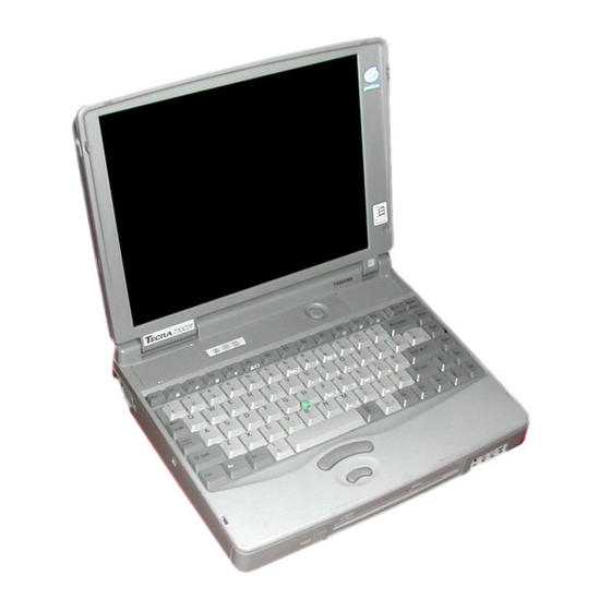
- Page 9 14.4 Kbps, and can be used as a speaker phone and Telephone Answering Machine (TAM). The computer is equipped with an RJ11 modem jack to connect directly to a telephone line. The 730CDT Personal Computer is shown in Figure 1-1 and its system configuration in Figure 1-2. 730CDT...
- Page 10 Figure 1-1 730CDT personal computer Figure 1-2 730CDT system unit configuration 730CDT...
-
Page 11: System Unit Block Diagram
Intel Pentium processor operating at 150 MHz and 3.1/3.3 volts. A math co-processor and 16 KB cache memory are integrated into the processor. Level-2 cache memory Data RAM: - 256 KB - Two 32K x 32-bit pipe-line burst synchronous SRAM chips - 3.3 volt operation - 8 ns access time 730CDT... - Page 12 5 volt operation 50 ns access time System controller Gate Array This gate array has the following functions: - CPU interface/control - Level-2 cache memory control - DRAM control - PCI master/slave interface - Write buffer (CPU-DRAM, CPU-PCI, PCI-DRAM) 730CDT...
- Page 13 Communication with power supply Communication with Desk Station V Plus Communication with EEPROM Communication register set - PWM control Beep volume - Speaker control - Universal I/O port - Q-SW control Modem interface Gate Array This gate array controls modem interface LSIs. 730CDT...
- Page 14 The controller provides simultaneous control of both the AccuPoint and a PS/2 mouse. Real Time Clock (RTC) One T9934 chip is used. The T9934 has 128 bytes of memory. Fourteen (14) bytes are used for the calendar and clock, and the remaining 114 bytes are used for system configuration data. 730CDT...
-
Page 15: Inch Floppy Disk Drive
Storage capacity (KB) Unformatted 2,000 1,000 Formatted 1,440 Number of heads Number of cylinders Access time (ms) Track to track Average Head settling time Recording track density (tpi) Data transfer rate (Kbps) Rotation speed (rpm) Recording method Modified Frequency Modulation (MFM) 730CDT... -
Page 16: Inch Hard Disk Drive
The removable HDD is a random access, nonvolatile storage device. It has a non-removable 2.5-inch magnetic disk and mini-winchester type magnetic heads. The 730CDT supports a 2.1 billion (2.02 GB) HDD. The HDD is shown in Figure 1-5, and its specifications are listed in Table 1-2. - Page 17 25-pin flat cable. The 730CDT AccuPoint pointer control stick, located in the center of the keyboard, provides convenient control of the cursor without requiring desk space for a mouse. The keyboard is shown in Figure 1-6.
- Page 18 Mode 1 Mode 2 1,026 ATAPI Burst (Mbytes/s) 8.33 (PIO mode 2) Access time (ms) Average Random Access Average Random Seek Average Full Stroke Access Rotation speed (rpm) 200 to 530 1,200 to 3,180 Data Buffer Capacity (Kbytes) 1-12 730CDT...
- Page 19 (FL), and an FL inverter board. 1.7.1 TFT Color LCD Module The 730CDT TFT color LCD is backlit supporting 1024x 768 pixels with a built-in display controller. The controller incorporates functions of the Video Graphics Array (VGA) and Super VGA (SVGA) for external displays.
- Page 20 Fluorescent Lamp (FL) Inverter Board The FL inverter board supplies a high frequency current to light the LCD’s Fluorescent Lamp.Specifications for the FL inverter are listed in Table 1-5. Table 1-5 FL inverter board specifications for 730CDT color LCD Status Item...
-
Page 21: Power Supply
Name voltage tolerance current Ripple (mA) (mV) System logic, FDD, HDD +5.0 ±5 3,400 Display panel, FL and PC card CPU, RAM, PC card +3.3 ±5 3,800 Flash ROM, PC card B12V +12.0 ±5 System logic +5.0 ±5 730CDT 1-15... - Page 22 2 when the system is powered on. Table 1-8 Time required for quick charges Status Charging time Quick charge 1 4 hours (power off) Quick charge 2 4.5 to 12.5 hours (power on) 1-16 730CDT...
- Page 23 AutoResume data is determined by the following priority: AC adapter > Main battery > Backup battery The backup battery is charged by the main battery or AC adapter. Table 1-9 lists the charging time and data preservation period of the backup battery. 730CDT 1-17...
- Page 24 Table 1-10 lists the charging time and data preser- vation period for the RTC battery. Table 1-10 RTC battery charging/data preservation time Status Time Charging Time (Power On) 40 hours Data preservation period (full charge) 1 month 1-18 730CDT...
-
Page 25: Troubleshooting
The following tools are necessary for implementing the troubleshooting procedures: Diagnostics Disk Phillips screwdriver (2 mm) Toshiba MS-DOS system disk(s) (You must install the following onto the disk: SYS.COM, FORMAT.COM, FDISK.COM and FDISK.EXE) A 2DD or 2HD formatted work disk used for floppy disk drive testing... -
Page 26: Troubleshooting Flowchart
® Verify with the customer that Toshiba MS-DOS or Toshiba Windows 95 is installed on the hard disk. Non-Toshiba operating systems can cause the computer to malfunc- tion. Make sure all optional equipment is disconnected from the computer. Make sure the floppy disk drive is empty. - Page 27 PCB procedures outlined in Section 2.4. If an error is detected on the floppy disk test, execute the floppy disk drive troubleshooting procedures outlined in Section 2.5. 730CDT...
- Page 28 Section 2.8. If an error is detected on the CD-ROM test, execute the CD-ROM drive trouble- shooting procedures outlined in Section 2.9. If an error is detected on the modem test, execute the modem troubleshooting procedures outlined in Section 2.10. 730CDT...
-
Page 29: Power Supply Troubleshooting
(even intervals) computer on battery power. Flashes yellow The power switch is pressed on when the battery level is low. Doesn't light Any condition other than those above. AutoResume Off will be executed soon. AutoResume Off has already been executed. 730CDT... - Page 30 An error code begins with the least significant digit. Example: Error code 12h (error codes are displayed in a hexadecimal format.) Check 1 Convert the DC IN icon blink pattern into the hexadecimal error code and com- pare it to the following tables. 730CDT...
- Page 31 Error code Meaning B3V voltage is over the maximum allowed limit. B3V voltage is below the minimum allowed limit. B3V does not start when the power supply is turned on. B3V is below the minimum allowed limit during suspend. 730CDT...
- Page 32 Chapter 4, Replacement Procedures. If the connector is not physically damaged, go to the following step: Check the Desk Station V Plus for malfunctions. Refer to the Desk Station V Plus maintenance manual for details. If the error still exists, go to Procedure 5. 730CDT...
- Page 33 Any of the connectors may be disconnected. Perform Check 1. Check 1 Make sure the AC adapter's cable and AC power cord are firmly plugged into the DC IN 15 V socket and wall outlet. If these cables are connected correctly, go to Check 2. 730CDT...
- Page 34 DC IN socket and wall outlet. If these cables are connected correctly, replace the AC power cord and AC adapter. Check 2 Make sure the battery is properly installed. If it is, replace it with a new battery. 2-10 730CDT...
-
Page 35: Check 4
Check 1 Replace the power supply board with a new one. If the power supply is still not functioning properly, perform Check 2. Check 2 Replace the system board with a new one. 730CDT 2-11... - Page 36 BIOS ROM. The IRT tests each IC on the system board and initializes it. If an error message is shown on the display, perform Check 1. If there is no error message, go to Procedure 2. If Toshiba MS-DOS or Toshiba Windows 95 is properly loaded, go to Procedure 3. Check 1 If any one of the following error messages display, press the F1 key (as the mes- sage instructs).
- Page 37 DMAC #2 ERROR (16) PIC #1 ERROR (17) PIC #2 ERROR (18) KBC ERROR (19) HDC ERROR (20) HDD #0 ERROR (21) HDD #1 ERROR (22) NO FDD ERROR (23) FDC ERROR (24) TIMER INTERRUPT ERROR (25) RTC UPDATE ERROR 730CDT 2-13...
-
Page 38: Check 1
IRT test ends. For example, when the printer port LED displays 1F and halts, the IRT test has already completed the Display initial- ization. In this case, the IRT indicates an error has been detected during the system memory test. 2-14 730CDT... - Page 39 EXTENDED MEMORY ERROR EXTENDED MEMORY PARITY ERROR DMA page register test DMA PAGE REGISTER ERROR DMAC test DMAC #X ERROR DMAC initialization — PIC test PIC #X ERROR Mouse initialization — KBC initialization KBC ERROR Boot password — 730CDT 2-15...
- Page 40 The printer port LED displays the IRT status and test status by turning lights on and off as an eight-digit binary value for resume mode. To use the printer port LED: Make sure the computer is in resume mode. Plug the printer port LED into the computer's parallel port. Turn on the computer. 2-16 730CDT...
- Page 41 Diagnostics, for more information on how to perform these tests. System test Memory test Printer test ASYNC test Real Timer test NDP test Expansion test Sound test Modem test If an error is detected during any of these tests, go to Procedure 5. 730CDT 2-17...
-
Page 42: Check 6
Replace the modem board with a new one. If the problem still exists, go to Check 6. Check 6 Replace the system board with a new one. NOTE: Refer to Chapter 4 for instructions on how to remove and replace each of the above items. 2-18 730CDT... - Page 43 If any other errors occur while executing the FDD diagnostics test, go to Check 1. Table 2-5 FDD error code and status (1/2) Code Status Bad command Address mark not found Write protected Record not found Media removed on dual attach card DMA overrun error DMA boundary error CRC error FDC error 730CDT 2-19...
- Page 44 Make sure the FDD cable is firmly connected to the external FDD port. FDD module System board Attachment case If this cable is disconnected, connect it to the system unit and repeat Procedure 2. If the FDD is still not functioning properly, perform Check 4. 2-20 730CDT...
- Page 45 Chapter 4, Replacement Procedures. If the FDD is still not functioning properly, perform Check 6. Check 6 Replace the system board with a new one following the steps outlined in Chapter 4, Replacement Procedures. 730CDT 2-21...
-
Page 46: Hard Disk Drive Troubleshooting
If MS-DOS 6.22 and Windows for Workgroups is selected, use the Master Diskette Creator (MDC) utility in the Toshiba Utility folder to back up the preinstalled software. After backing up the preinstalled software, use the BACKUP command in the Toshiba Companion Utility to back up the entire disk, including the user's files. - Page 47 Procedure 1 Partition Check Insert the Toshiba MS-DOS system disk into the disk drive, turn on the computer, then perform the following checks: Check 1 Type C: and press Enter. If you cannot change to drive C, go to Check 2. If you can change to drive C, go to Procedure 2.
- Page 48 HDD. If the following message appears on the display, the HDD is formatted. Format complete If any other error message appears on the display, refer to the Toshiba MS-DOS Manual for more information and perform Check 2. 2-24...
- Page 49 HDC overrun (DRQ) DMA boundary error Bad sector error Bad track error ECC error ECC recover enable HDC error Seek error Time out error Drive not ready Undefined error Write fault Status error Access time out error Data compare error 730CDT 2-25...
- Page 50 Replace the flexible cable with a new one following the instructions outlined in Chapter 4, Replacement Procedures. If the HDD is still not functioning properly, perform Check 3. Check 3 Replace the system board with a new one following the instructions outlined in Chapter 4, Replacement Procedures. 2-26 730CDT...
-
Page 51: Keyboard Troubleshooting
Chapter 4, Replacement Procedures for more information. If the keyboard is still not functioning properly, perform Check 3. Check 3 The keyboard controller on the system board may be damaged. Replace the system board with a new one. Refer to Chapter 4, Replacement Procedures for more information. 730CDT 2-27... -
Page 52: Display Troubleshooting
Figure 2-3. Any of these cables may be discon- nected. Disassemble the display unit and check the cable connections shown in Figure 2-3. Refer to Chapter 4, Replacement Procedures, for more information about how to disassemble the computer. 2-28 730CDT... - Page 53 Replace the FL inverter board with a new one and test the display again. If the problem still exists, perform Check 3. Check 3 Replace the LCD module with a new one and test the display again. If the problem still exists, perform Check 4. 730CDT 2-29...
- Page 54 Check 5 Replace the display cable with a new one and test the display again. If the problem still exists, perform Check 6. Check 6 The system board may be damaged. Replace the system board with a new one. 2-30 730CDT...
- Page 55 The CD-ROM drive Diagnostic Test program is stored on the computer's Diagnostics Disk. Insert a test CD (Toshiba-EMI Test Disc TDY-03) into the CD-ROM drive. Insert the Diag- nostics disk into the computer’s floppy disk drive, turn on the computer, and run the test.
- Page 56 Chapter 4. If the CD-ROM drive is still not functioning properly, perform Check 5. Check 5 Replace the system board with a new one following the steps outlined in Chapter 2-32 730CDT...
- Page 57 Make sure DAA board PJ1 is connected firmly to the modem I/F board PJ1 and that the modem I/F board PJ2 is connected firmly to the system board PJ605. DAA board PJ1 Modem I/F board PJ605 System board 730CDT 2-33...
- Page 58 Replace the modem I/F board with a new one following the steps outlined in Chapter 4. If the DAA board is still not functioning properly, perform Check 4. Check 4 Replace the system board with a new one following the steps outlined in Chapter 2-34 730CDT...
-
Page 59: The Diagnostic Test
The DIAGNOSTICS TEST option contains the following functional tests: SYSTEM TEST MEMORY TEST KEYBOARD TEST DISPLAY TEST FLOPPY DISK TEST PRINTER TEST ASYNC TEST HARD DISK TEST REAL TIMER TEST NDP TEST EXPANSION TEST SOUND TEST CD-ROM TEST MODEM TEST 730CDT... - Page 60 A printer wraparound connector for the printer wraparound test (printer test) An RS-232-C wraparound connector for the RS-232-C port wraparound test (ASYNC test) A CD test media (Toshiba-EMI test disk TDY-03, and music CD for the CD-ROM test) External CRT (all tests)
-
Page 61: Executing The Diagnostic Test
Executing the Diagnostic Test Toshiba MS-DOS is required to run the DIAGNOSTICS program. To start the program follow the steps listed below: Insert the Diagnostics Disk into the computer’s floppy disk drive and turn on the computer. (The Diagnostics Disk contains the MS-DOS boot files.) -
Page 62: Table Of Contents
TOSHIBA personal computer xxx DIAGNOSTICS version X.XX (c) copyright TOSHIBA Corp. 19XX DIAGNOSTIC TEST menu: 1 - SYSTEM TEST 2 - MEMORY TEST 3 - KEYBOARD TEST 4 - DISPLAY TEST 5 - FLOPPY DISK TEST 6 - PRINTER TEST... - Page 63 Selecting NO for ERROR STOP keeps the test running even if an error is found. Table 3-1 in Section 3.3 lists the function of each test on the subtest menu. Table 3-2 in Section 3.18 lists the error codes and error status for each error. 730CDT...
-
Page 64: Subtest Names
VRAM read/write for VGA Gradation for VGA Gradation for LCD Gradation & Mode test for VGA All dot on/off for LCD “H” pattern display Sequential read Sequential read/write Random address/data Write specified address Read specified address PRINTER Ripple pattern Function Wraparound 730CDT... - Page 65 PCMCIA wraparound DS bus wraparound (Not used) RGB monitor ID (Not used) Joystick (Not used) Joystick wraparound (Not used) SOUND CODEC (Recording/Playback) FM-Synthesizer SIN-Wave Playback CODEC (Line In/Out) CD-ROM Sequential read Read specified address Random address/data Playback Music MODEM Modem 730CDT...
-
Page 66: System Test
If the data indicates the connector is open or shorted, it displays an error message. Subtest 06 Quick charge This subtest determines whether the battery pack can be quick charged. Refer to Chapter 2 for a list of result codes. 730CDT... -
Page 67: Memory Test
Also, HIMEM.SYS must be deleted from the CONFIG.SYS file. This subtest writes constant data and address data to extended memory (maxi- mum address 100000h), then reads new data and compares the result with the original data. The constant data is FFh, AAh, 55h, and 00h. 730CDT... - Page 68 ('7000':'Program' size to '7000':'7FFF' (32 KB)) to check the hit-miss ratio (on/off status) for L2 cache memory. One test takes three seconds. Number of misses < Number of hits → OK Number of misses ≥ Number of hits → Fail 3-10 730CDT...
-
Page 69: Keyboard Test
The Ins, Caps Lock, Num Lock, Scroll Lock, Alt, Ctrl, Left Shift, and Right Shift keys are displayed in reverse video when pressed. The scan codes, character codes, and key top names are listed in Appendix D. 730CDT 3-11... - Page 70 If an IPS switch is pressed, the <BUTTON> display alternates between black and white. Also, the parameters appear on the right side of the display. If two IPS switches are pressed at the same time, the subtest menu is displayed. 3-12 730CDT...
- Page 71 < PARAMETER > STATUS:0008h X-RATE:0000h Y-RATE:0000h < BUTTON > << PRESS BUTTON1 + BUTTON2 THEN END >> There are eight directions of arrow marks as shown below. When a button is pressed, the display alternates as shown below. < > 730CDT 3-13...
- Page 72 To exit this subtest and return to the DISPLAY TEST menu, press Ctrl + Break. Subtest 03 Gradation for LCD This subtest displays eight colors: red, semi-red, green, semi-green, blue, semi-blue, white, and semi-white. Each color is displayed full screen for three seconds. 3-14 730CDT...
- Page 73 3, 12, 13, 43, 52 1024 x 768 3, 12, 13, 45 The display below appears on the screen when this subtest is executed. Pressing Enter changes the size of the displayed image. Pressing Enter changes the size of the displayed image. 730CDT 3-15...
- Page 74 All dot on /off for LCD This subtest displays an all-white screen (all dot on) for three seconds then an all-black screen (all dot off) for three seconds. To exit this subtest and return to the DISPLAY TEST menu, press Ctrl + Break. 3-16 730CDT...
- Page 75 This subtest displays a full screen of "H" patterns. HHHHHHHHHHHHHHHHHHHHHHHHHHHHHHHHHHHHHHHHHHHHHHHHHH HHHHHHHHHHHHHHHHHHHHHHHHHHHHHHHHHHHHHHHHHHHHHHHHHH HHHHHHHHHHHHHHHHHHHHHHHHHHHHHHHHHHHHHHHHHHHHHHHHHH HHHHHHHHHHHHHHHHHHHHHHHHHHHHHHHHHHHHHHHHHHHHHHHHHH HHHHHHHHHHHHHHHHHHHHHHHHHHHHHHHHHHHHHHHHHHHHHHHHHH HHHHHHHHHHHHHHHHHHHHHHHHHHHHHHHHHHHHHHHHHHHHHHHHHH HHHHHHHHHHHHHHHHHHHHHHHHHHHHHHHHHHHHHHHHHHHHHHHHHH HHHHHHHHHHHHHHHHHHHHHHHHHHHHHHHHHHHHHHHHHHHHHHHHHH HHHHHHHHHHHHHHHHHHHHHHHHHHHHHHHHHHHHHHHHHHHHHHHHHH HHHHHHHHHHHHHHHHHHHHHHHHHHHHHHHHHHHHHHHHHHHHHHHHHH HHHHHHHHHHHHHHHHHHHHHHHHHHHHHHHHHHHHHHHHHHHHHHHHHH HHHHHHHHHHHHHHHHHHHHHHHHHHHHHHHHHHHHHHHHHHHHHHHHHH HHHHHHHHHHHHHHHHHHHHHHHHHHHHHHHHHHHHHHHHHHHHHHHHHH HHHHHHHHHHHHHHHHHHHHHHHHHHHHHHHHHHHHHHHHHHHHHHHHHH HHHHHHHHHHHHHHHHHHHHHHHHHHHHHHHHHHHHHHHHHHHHHHHHHH To exit this subtest and return to the DISPLAY TEST menu, press Ctrl + Break. 730CDT 3-17...
-
Page 76: Floppy Disk Test
The following tracks are read accord- ing to the media type in the floppy disk drive: Double-sided, double-density (2D): Tracks 0 to 39. Double-sided, double-density, double-track (2DD), and double-sided, high-density, double-track (2HD): Tracks 0 to 79. 3-18 730CDT... - Page 77 Subtest 01. The data is then read and compared to the original data. Subtest 04 Write Specified Address This subtest writes specified data to a specified track, head, and address. Subtest 05 Read Specified Address This subtest reads data from a specified track, head, and address. 730CDT 3-19...
-
Page 78: Printer Test
This subtest is for IBM-compatible printers and tests the following functions: • Normal print • Double width print • Compressed print • Emphasized print • Double strike print • All characters print The subtest prints the various print types shown below: 3-20 730CDT... - Page 79 The printer wraparound connector (34M741986G01) wiring diagram is shown in Appendix F. This subtest checks the output and bidirectional modes of the data control and status lines through the printer wraparound connector. 730CDT 3-21...
-
Page 80: Async Test
"receive" (Subtest 03). The wiring diagram for the RS-232-C direct cable is shown in Appendix F. This subtest sends 20h through 7Eh data to the receive side, then receives the sent data and compares it to the original data. 3-22 730CDT... - Page 81 SIR port. Subtest 07 SIR point to point (Receive) This subtest, used with Subtest 06 described above, receives the data from the send side, then sends the received data through the SIR port. 730CDT 3-23...
-
Page 82: Hard Disk Test
If MS-DOS 6.22 and Windows for Workgroups is selected, use the Master Diskette Creator (MDC) utility located in the Toshiba Utility folder to back up the preinstalled software. Now use the BACKUP command from the Toshiba Companion Utility to back up the entire disk, including the user's files. - Page 83 • Forward sequential • Reverse sequential • Random Subtest 03 Random Address/Data This subtest writes random data to random addresses on the HDD cylinder, head and sector. This data is then read and compared to the original data. 730CDT 3-25...
- Page 84 This subtest writes specified 2-byte data to all of the cylinders on the HDD. Subtest 10 W-R-C specified address This subtest writes data to a specified cylinder and head on the HDD, then reads the data and compares it to the original data. 3-26 730CDT...
-
Page 85: Real Timer Test
Writes 1-bit of "off" data to address 0Eh through 80h Writes the data pattern AAh and 55h to the RTC 114-byte memory (address 0Eh to 7Fh) The subtest then reads and compares this data with the original data. To exit, press Ctrl + Break . 730CDT 3-27... - Page 86 Current date : 12-31-1995 Current time : 23:59:58 Pressing Enter displays the following: Current date : 01-01-1996 Current time : 00:00:00 PRESS [Enter] KEY TO EXIT TEST Press Ctrl + Break to exit. 3-28 730CDT...
-
Page 87: Ndp Test
The NDP test contains one subtest that tests the computer's NDP functions. Subtest 01 This test checks the following functions of the coprocessor: Control word Status word Addition Multiplication Press Ctrl + Break to exit. 730CDT 3-29... -
Page 88: Expansion Test
Good Contents 00001 Address line 00001 REG#, CE#1, CE#2 nn=A0, 90, 80, 00 00002 Data line ww=write data, rr=read data 00003 –– –– Speaker line 00004 40, 80 Wait line (40<xx<80) 00005 Other lines (BSY#, BVD1) nn=21, 00 3-30 730CDT... -
Page 89: Sound Test
Load the file AD1848L.COM. Connect a sound source such as a CD player or stereo to the line-in port. Connect an output device such as an amplifier for the internal speaker or a radio/cassette player to the line-out port. 730CDT 3-31... - Page 90 After making the connections, a dialog box will display. Press Enter to play a recorded sound. About three seconds after the recorded sound is played, the dialog box will display again. 3-32 730CDT...
-
Page 91: Cd-Rom Test
The CD-ROM Test contains four subtests that test the computer's CD-ROM functions. NOTE: Make sure the CD-ROM driver (CDROMDRV.COM) is installed, then insert the test media CD (Toshiba-EMI Test Disk TDY-03) before executing this test.) Subtest 01... -
Page 92: Modem Test
NOTE: Before you conduct the Terminal Test, connect the DAA module to a telephone using a modular cable. When you have connected the DAA module to a telephone, test the connection by calling the line from another phone. 3-34 730CDT... - Page 93 Select the COM port (the same one selected in the Hardware Setup program). The following screen displays: Baud rate (2:300,,4:1200,5:2400,6:9600,7:14400,8:19200,9:38400)? Select the Baud rate and press Enter . The selected test is executed. Function 9 exits this subtest and returns to the SUBTEST menu. 730CDT 3-35...
-
Page 94: Error Codes And Error Status Names
Fault Select Line Out Of Paper Power Off Busy Line Async DSR On Time Out CTS On Time Out RX-READY Time Out TX-BUFFER Full Time Out Parity Error Framing Error Overrun Error Line Status Error Modem Status Error 3-36 730CDT... - Page 95 BSY# Line Error BVD1 Line Error No PCMCIA CD-ROM Bad Command Illegal Length Unit Attention Media Change Request Media Detected Additional Sense Boundary Error Corrected Data Error Drive Not Ready Seek Error Time Out Reset Error Address Error 730CDT 3-37...
-
Page 96: Hard Disk Test Detail Status
“0” --- Note used (Corrected data) “1” --- A correctable data error was corrected. “0” --- Not used (Index) “1” --- The Index was sensed. “0” --- Normal (Error) “1” --- The previous command was terminated with an error. 3-38 730CDT... - Page 97 “1” Illegal command error or a drive status error occurred. TK00 “0” The hard disk has found track 0 during a recalibrate command. (Track 0) “1” The hard disk could not find track 0 during a recalibrate command. —— Not used 730CDT 3-39...
-
Page 98: Hard Disk Format
If MS-DOS 6.22 and Windows for Workgroups is selected, use the Master Diskette Creator (MDC) utility located in the Toshiba Utility folder to back up the preinstalled software. Now use the BACKUP command from the Toshiba Companion Utility to back up the entire disk, including the user's files. - Page 99 This option searches the hard disk for bad tracks by reading data to all the tracks on the hard disk. A list of bad tracks is displayed when the program is complete. If an error other than a bad track is detected, the program is automatically termi- nated. 730CDT 3-41...
- Page 100 3.20.2 Operations NOTE: After the HDD has been formatted, execute the Toshiba MS-DOS FDISK command to partition the HDD. Next, execute the Toshiba MS-DOS FORMAT command. Refer to the Toshiba MS-DOS manual for more information about using these commands. Selecting 2 and pressing Enter in the DIAGNOSTIC menu, displays the following submenu: DIAGNOSTICS - HARD DISK FORMAT : VX.XX...
- Page 101 Drive number select (1:#1, 2:#2) ? Interleave number (1 / 1 - 8) ? Press [Cylinder number (dddd)] ? Press [Head number (dd)] ? Press Enter to return to the Hard Disk Format menu. 730CDT 3-43...
- Page 102 To initiate the subtest, enter the drive number at the prompt shown below. Drive number select (1:#1, 2:#2) ? Bad tracks will be displayed in the following format: [[cylinder, head = 0123 03]] Press Enter to return to the Hard Disk Format menu. 3-44 730CDT...
-
Page 103: Head Cleaning
Remove the Diagnostics Disk from the FDD, insert the cleaning disk, and press Enter . When the "cleaning start" message displays, the FDD head cleaning has begun. The display automatically returns to the DIAGNOSTIC menu when the program completes. 730CDT 3-45... -
Page 104: Log Utilities
001 FDD 01 0000 180 00001 00 00 FDD - TIME OUT ERROR Address Error status Pass count HDC status Subtest number Read data Test name Write data Error count Error status name [[1:Next,2:Prev,3:Exit,4:Clear,5:Print,6:FD Log Read,7:FD Log Write]] 3-46 730CDT... - Page 105 The 7 key writes the log information to a floppy disk. 3. If an “error retry OK" condition occurs, a capital “R” is placed at the beginning of the error status. It is not, however, added to the error count. 730CDT 3-47...
-
Page 106: Running Test
Select Y or N and press Enter . The following message displays: Serial #A wrap around test (Y/N) ? Selecting Y (yes) executes the ASYNC wraparound test. An RS-232-C wrap- around connector must be connected to the computer's serial port to properly execute this test. 3-48 730CDT... - Page 107 Select Yes or No, and press Enter . The following message will display: Mount the work disk(s) on the drive(s), then press [Enter] key. [Warning : The contents of the disk(s), will be destroyed.] This program executes continuously. To terminate the program, press Ctrl + Break . 730CDT 3-49...
-
Page 108: Floppy Disk Drive Utilities
FDD and HDD. FORMAT NOTE: This program is only for testing a floppy disk drive. This option is different from the Toshiba MS-DOS FORMAT command. This program can format a 5.25-inch or 3.5-inch floppy disk in the following formats: 2D: Double-sided, double-density, 48/67.5 TPI, MFM mode, 512 bytes, 9 sectors/track. - Page 109 When COPY is selected, the following message displays: FLOPPY DISK FORMAT & COPY : VX.XX Type select (0:2DD-2DD,1:2D-2D,2:2D-2HD,3:2HD-2HD) ? Selecting a media/drive type number will display a message similar to the following one: Insert source disk into drive A: Press any key when ready. 730CDT 3-51...
- Page 110 If 2 is selected, the following message displays: Select drive number (1:C, 2:D) ? After selecting the HDD, the display will go to step (f). The following message displays: Format type select (1:2DD, 2:2D, 3:2HD) ? Select a format type. The following message displays: 3-52 730CDT...
- Page 111 The following message displays: —— Max. address —— [Track ] = XXXX [ Head ] = XX [Sector] = XX Track number ?? Set the track number you want to dump. The system will access the disk and dump a list. 730CDT 3-53...
-
Page 112: System Configuration
* - 1 ASYNC ADAPTER * - 1 HARD DISK DRIVE(S) * - 1 PRINTER ADAPTER * - XXXMB + XXXXKB EXTENDED MEMORY * - 1 MATH CO-PROCESSOR Press [Enter] Key Press Enter to return to the DIAGNOSTIC menu. 3-54 730CDT... - Page 113 Auto Power On Alarm Volume System Beep Panel Power On/Off Keyboard Boot Priority Pointing Devices PC Card Controller Mode Display I/O Ports Serial Port Infrared Port Built-in Modem Port Parallel Port Sound System PCI Bus Drives I/O Floppy Disk I/O 730CDT 3-55...
-
Page 114: Accessing The Setup Program
Space, BkSp : Change values PgDn, PgUp : Change pages Esc: Exit without saving Home: Set default values End: Save changes and Exit NOTE: The Panel Power On/Off item appears only when the computer is in Resume mode. 3-56 730CDT... - Page 115 To show the factory preset configuration, press Home . To accept the default settings, press End and then Y. NOTE: When you execute the default settings, the following settings are not changed: HDD Mode Password Sound System: I/O Address, Interrupt Level, DMA Write Policy 730CDT 3-57...
- Page 116 NOTE: When starting the computer in Resume mode, the last configuration is remembered. If data does not appear on the display as selected after starting Resume mode, press Fn+F5. This changes the display setting in the order of internal LCD to simultaneous to external CRT. 3-58 730CDT...
- Page 117 504MB. Not used HDD is not installed. To display the capacity of the hard disk, use the CHKDSK command. See your DOS documentation for details on using CHKDSK. 730CDT 3-59...
- Page 118 Battery Save Mode: Low Power (Long Life) or Full Power (Normal Life). For details, see Battery Save Options below. Battery Save Options The following set of options can be selected in the User Setting submenu, which is one of the Battery Save Mode options. 3-60 730CDT...
- Page 119 Disables the HDD automatic power off function. xx Min. Automatically turns off power to the hard disk drive if it is not used for the duration set. The duration xx can be set to 1, 3, 5, 10, 15, 20, or 30 minutes. 730CDT 3-61...
- Page 120 This option lets you choose between AutoResume and boot mode. You can also set this option using hot keys. AutoResume is effective with either the internal LCD or with an external monitor. Boot Turns on boot mode (Default). Resume Turns on the AutoResume feature. 3-62 730CDT...
- Page 121 Disabled, the computer will be powered on at the same time every day. Press ↓ to move the cursor to the right and ↑ to move the cursor to the left when you set the date and time. 730CDT 3-63...
- Page 122 LOW BATTERY Alarm Enabled Panel Close Alarm Enabled Enabled Enables the feature (Default). Disabled Disables the feature. System Beep Use this feature to enable or disable the system beep. Enabled Enables the feature (Default). Disabled Disables the feature. 3-64 730CDT...
- Page 123 Right Ctrl + Right Alt* Left Alt + Left Shift Right Alt + Right Shift Left Alt + Caps Lock * If these selections are made, you cannot warm boot the system by pressing Ctrl + Alt + Del. 730CDT 3-65...
- Page 124 PC Card Controller Mode Use this option to set the PC card controller mode. PCIC Compatible Used for the PCMCIA R2.01 and ZV port card (Default). CardBus/16bit Used for the PC 16 multi-function card, CardBus card and ZV port card. 3-66 730CDT...
- Page 125 (Others settings are made automatically by plug-and- play operating systems) NOTE: If the setting for the serial port is the same as that for the infrared or Modem port, the infrared or Modem port is automatically set to disabled. 730CDT 3-67...
- Page 126 Interrupt level I/O address COM1 3F8H COM2 2F8H (Modem port default) COM3 3E8H COM3 3E8H COM3 3E8H COM4 2E8H COM4 2E8H COM4 2E8H Not used (Disables port) Others (Others settings are made automatically by plug-and- play operating systems) 3-68 730CDT...
- Page 127 The options for this setting are ECP (default) and Standard Bi-Directional. Options Mode = Channel 3 For most printers, the port should be set to ECP. With other parallel de- vices, the setting should be Standard Bi-Directional. 730CDT 3-69...
- Page 128 220h (Default), 240h Synthesizer I/O address You cannot change this value. WSS & SBPro IRQ level Sets the WSS & SBPro IRQ level for the sound system from the following options: IRQ5 (Default) , IRQ7, IRQ9, IRQ11, IRQ15 3-70 730CDT...
- Page 129 No PCI card is installed in the Desk Station V Plus. The system cannot assign an interrupt level to the PCI bus. The PC Card Controller Mode is not set to CardBus/16Bit in TSETUP. PCI bus = IRQ Not Used 730CDT 3-71...
- Page 130 Floppy disk I/O Displays the address, internal level and channel settings for the diskette drive. (3F2H/IRQ6/CH2) The FDD is ready for use. Others Other setting made automatically by plug- and play operating system. Not used Disables the diskette drive. 3-72 730CDT...
- Page 131 Hard Disk Drive Upper Cover and Keyboard DAA module Display Assembly, Jack Display Mask FL Inverter Board Board, and Modem Board LCD Module IPS (FLXIP*) Board , RTC Microphone Battery, and Backup Battery Power supply (FLXPS*) Board System (FLXSY*) Board 730CDT...
-
Page 132: Safety Precautions
DANGER: 1. Always use the lithium ion battery pack or backup battery that is authorized by Toshiba or compatible with the unit. Since other battery packs have different specifications, they may be incompatible with the unit and may burst or explode. Heating or disassembling the battery pack could cause leakage of alkaline solution. -
Page 133: Before You Begin
The computer contains many sharp edges and corners, so be careful not to injure yourself. After you have replaced an FRU, make sure the computer is functioning properly by performing the appropriate test on the FRU you have fixed or replaced. 730CDT... -
Page 134: Disassembly Procedures
FRU. After installing an FRU in the computer, confirm that the FRU and the computer are functioning properly. 730CDT... -
Page 135: Tools And Equipment
Overtightening can damage components and screws; undertightening can result in electrical shorts or other damage if screws or components become loose. 0.22 N·m (2.2 kgf·cm) M2.5 0.36 N·m (3.5 kgf·cm) 0.22 N·m (2.2 kgf·cm) 0.3 N·m (3.1 kgf·cm) or less LCD (internal use) 0.175 N·m ±0.02 N·m 730CDT... -
Page 136: Battery Pack
Figure 4-1 Removing the battery NOTE: For environmental reasons, do not throw away a spent battery pack. Please return spent battery packs to Toshiba. Remove the battery cover. Carefully push up slightly as you slide the cover past the unlock position. -
Page 137: Installing The Battery Pack
To install the battery pack, follow the steps below and refer to Figure 4-1. WARNING: The battery is a lithium ion battery. The battery can explode if not properly replaced, used, handled, or disposed of. Use only batteries recommended by Toshiba as replacements. - Page 138 Grasp the memory card on the right edge toward the connector, or if a plastic tab is present, lift up on the plastic tab to disengage the connectors, then grasp the module by the edges and remove it. 730CDT...
- Page 139 Secure the module to the brace with two M2x10 screws. Fold down the plastic tab, if it is present, and lay the memory slot cover in place. Secure it with two M2x3 silver screws. Install the battery pack as described in Section 4.2. 730CDT...
- Page 140 Remove the battery pack as described in Section 4.2. Open the PC slot cover. Figure 4-4 Removing the lower PC card Press the eject button for the upper and/or lower card. Grasp the PC card and remove it. 4-10 730CDT...
-
Page 141: Installing An Optional Pc Card
Insert the PC card. Press gently to ensure a firm connection. Figure 4-5 Installing the lower PC card Close the PC slot cover. Install the optional memory module and battery pack as described in Sections 4.3 and 4.2. 730CDT 4-11... - Page 142 Slide the LED indicator cover to the left to free it from its latches. Rotate the cover up. Pull the release handle to pop the drive out slightly. Grasp the FDD and pull it out. Figure 4-6 Removing the FDD 4-12 730CDT...
- Page 143 Figure 4-7 Removing the FDD screws Lift off the plate, unseat the flexible cable connector from the lower plastic cover, and lift out the FDD. Figure 4-8 Removing the plate 730CDT 4-13...
- Page 144 M2x6 silver screws. Turn the computer upside down. Make sure that the LED indicator cover is facing up, insert the FDD into the computer, and gently press until it locks into place. 4-14 730CDT...
- Page 145 Close the LED indicator cover. Slide the cover to the right to engage the latches. Figure 4-10 Installing the FDD Install the optional memory module, optional PC card, and battery pack as described in Sections 4.4, 4.3, and 4.2. 730CDT 4-15...
- Page 146 Slide the LED indicator cover to the left to free it from the latches. Rotate the cover up. Pull the release handle to pop the drive out slightly. Grasp the drive and pull it out. Figure 4-11 Removing the CD-ROM drive 4-16 730CDT...
- Page 147 CD-ROM drive. Figure 4-12 Removing the CD-ROM screws Slide the drive partially out of the frame. Remove the drive from the cover and cable cover, then disconnect the cable connector. Figure 4-13 Removing the CD-ROM 730CDT 4-17...
- Page 148 Close the LED indicator cover. Slide the cover to the right to engage the latches. Figure 4-14 Installing the CD-ROM drive Install the optional PC card, optional memory module, and battery pack as described in Sections 4.4, 4.3, and 4.2. 4-18 730CDT...
- Page 149 Peel off the VOID seal at the top, and remove four flat M3x4 screws securing the cover to the pack. Slide the cover forward slightly (about 2 cm) and lift it off. Figure 4-16 Removing the HDD screws 730CDT 4-19...
- Page 150 Turn the computer upside down, slide the LED indicator cover to the left, and rotate the cover up. Insert the HDD, VOID label side up, and press to ensure a firm connection. Install the optional PC card, optional memory module, and battery pack as described in Sections 4.4 back through 4.2. 4-20 730CDT...
- Page 151 Figure 4-18 Removing screws from the back of the computer Lift up slightly on the upper cover at the back of the computer so it can easily clear the audio jacks. Open the display panel and lay the display back fully. 730CDT 4-21...
- Page 152 Remove one left M2.5x6 and one right M2.5x4 screw securing the metal brace near the keyboard and AccuPoint mouse connector, then remove the brace. Remove one M2.5x6 screw securing the display ground wire and metal cover, then lift out the cover. Figure 4-20 Removing the metal brace and cover 4-22 730CDT...
- Page 153 Seat the metal cover and secure it and the display ground wire with one M2.5x6 screw. Secure the metal keyboard brace to the keyboard with one M2.5x6 screw and one M2.5x4 screw. Seat the Volume knob and white plastic washer, then replace the tape over the display cables. 730CDT 4-23...
- Page 154 Secure four M2.5x4 silver screws on the back of the computer. Replace the right and left connector covers on the back of the computer. Install the HDD, CD-ROM drive or FDD, optional memory module, optional PC card, and battery pack as described in Sections 4.7 back through 4.2. 4-24 730CDT...
- Page 155 CD-ROM drive, HDD, and upper cover and keyboard as described in Sections 4.2 through 4.8. Carefully remove the DAA module lower cover. Remove two M2.5x4 silver screws securing the DAA module jack cover and remove the jack cover. Figure 4-22 Removing the lower cover screws 730CDT 4-25...
- Page 156 Pull out the DAA module. Figure 4-23 Removing the DAA module screws Remove three M2.5x4 screws securing the DAA module's metal cover and remove the cover, taking care to clear the guide post. Figure 4-24 Removing the DAA module metal cover screws 4-26 730CDT...
- Page 157 Seat the jack cover and secure it with two M2.5x4 screws. Replace the DAA module cover. Install the upper cover and keyboard, HDD, CD-ROM drive or FDD, optional memory module, optional PC card, and battery pack as described in Sections 4.8 through 4.2. 730CDT 4-27...
-
Page 158: Display Mask
Carefully insert your fingers between the mask and the LCD panel and pry open the latches. Start with five latches across the top of the display mask. Continue releasing the mask along the sides (four latches on each side), then at the bottom (four latches). 4-28 730CDT... - Page 159 Secure the cover with two M2.5x6 screws at the hinges. Attach the two mask seals to cover the screws. Install the optional memory module, optional PC card, and battery pack as described in Sections 4.4, 4.3, and 4.2. 730CDT 4-29...
-
Page 160: Fl Inverter Board
CN1 and the HV cable from CN2. Note: You may wish to place a binder and form pad under the display to provide additional stability while performing these steps. Figure 4-28 Removing the FL inverter board 4-30 730CDT... - Page 161 Replace the FL inverter board and secure it with two M2.5x6 screw. Install the display mask, optional memory module, optional PC card, and battery pack as described in Sections 4.10, 4.4, 4.3, and 4.2. 730CDT 4-31...
-
Page 162: Lcd Module
Remove the tape, then carefully rotate the LCD module from right to left out of the display cover and disconnect the LCD cable from CN1 on the LCD module. Note the position of the noise-reduction gasket. Figure 4-29 Removing the LCD module 4-32 730CDT... - Page 163 Seat the LCD module and then secure it to the LCD cover with four M2.5x6 screws. Install the FL inverter board, display mask, optional memory module, optional PC card, and battery pack as described in Sections 4.11, 4.10, 4.4, 4.3, and 4.2. 730CDT 4-33...
- Page 164 Remove one M2.5x6 ground screw in the top cover cable channel and disconnect the FL Inverter cable from PJ703 on the IPS board. Remove the tape from the back cover and covering the cable, and lift out the FL inverter cable. Figure 4-30 Removing the ground cable screws 4-34 730CDT...
- Page 165 Secure the two ground cables to the right hinge with two M2.5x6 screws. Install the display mask, upper cover, optional memory module, optional PC card, and battery pack as described in Sections 4.12, 4.11, 4.10, 4.4, 4.3, and 4.2. 730CDT 4-35...
- Page 166 Turn the computer upside down and remove two M2.5x6 silver screws from the battery pack slot, two M2x3 silver screws from the selectable bay, and three M2.5x20 silver screws from the computer base. 4-36 730CDT...
- Page 167 Disconnect the speaker cable from PJ6 on the jack board and remove the right speaker. Disconnect the microphone cable from PJ207 on the jack board. Remove one M2.5x6 screw securing the ground cable to the computer. This screw is somewhat hidden under the FL Inverter cable near the right hinge. 730CDT 4-37...
- Page 168 Disconnect the FL inverter cable from PJ703 on the IPS board. Figure 4-33 Removing additional cables Remove the volume control knob. Release nine latches securing the keyboard base: three on the right, two in front, and four on the left. 4-38 730CDT...
- Page 169 Carefully rotate the keyboard base backward about 90 degrees and slip the video cable out of the slot on the keyboard base. Lift off the keyboard base and display assembly. Figure 4-35 Removing the keyboard base and display assembly 730CDT 4-39...
- Page 170 Figure 4-36 Removing the metal cover Disconnect the jack board connector (PJ201) from the modem board connector (PJ3) to remove the jack board. Be careful to note the position of the mylar covering on the jack board. Figure 4-37 Disconnecting the jack board 4-40 730CDT...
- Page 171 Figure 4-38 Removing the modem board Disconnect the video cable from PJ603 on the system board. Disconnect the fan cable from PJ16 on the system board. Figure 4-39 Disconnecting the video cable and fan cable Remove the keyboard base and display assembly. 730CDT 4-41...
- Page 172 M2.5x20 silver screws in the computer base. Install the LCD module, FL Inverter board, display mask, DAA module, upper cover and keyboard, HDD, CD-ROM drive or FDD, optional memory module, optional PC card, and battery pack as described in Sections 4.13 through 4.2. 4-42 730CDT...
- Page 173 4.15 IPS Board, RTC Battery, and Backup Battery WARNING: If you replace the RTC battery or sub-battery, be sure to use only batteries recommended by Toshiba. Installation of the wrong battery can cause the battery to explode or otherwise cause damage.
- Page 174 Remove the rubber bar securing the RTC and backup battery cables, and the tape securing the batteries themselves. Note: Take note of the cable routing and tape placement before removing them. Lift out the RTC and backup batteries. Remove the insulator. Figure 4-41 Removing the RTC and backup batteries 4-44 730CDT...
- Page 175 Install the display assembly, jack board, modem board, speaker, LCD module, FL Inverter board, display mask, DAA module, upper cover and keyboard, HDD, CD-ROM drive or FDD, optional memory module, optional PC card, and battery pack as described in Sections 4.14 back through 4.2. 730CDT 4-45...
- Page 176 PJ11 on the system board, and remove the power supply board (directing pressure near the AC jack). Be sure to note how the selectable bay connector tabs are routed on top of the power supply board. Figure 4-42 Removing the power supply board 4-46 730CDT...
- Page 177 FL Inverter board, LCD module, DAA module, upper cover and keyboard, HDD, CD-ROM drive or FDD, optional memory module, optional PC card, and battery pack as described in Sections 4.15 back through 4.2. 730CDT 4-47...
-
Page 178: System Board
PJ604 on the system board, or lift the pressure connectors to quickly remove them, and then remove the selectable bay connector. Lift out the plastic brace for the HDD connector. Lift the pressure connectors and disconnect the flexible cable from PJ602 on the system board. 4-48 730CDT... - Page 179 CPU, one M2.5x8 screw between the PC card connector and the metal back panel, and one M2.5x6 screw in the frame hole on the other side of the HDD slot. Finally, remove two M2.5x6 screws in the selectable bay slot. Figure 4-45 Removing the frame and system board screws 730CDT 4-49...
- Page 180 Remove one M2.5x6 screw securing the system board to the frame and separate the system board from the frame. Figure 4-47 Separating the system board, heat sink, and frame 4-50 730CDT...
- Page 181 HDD slot. Finally, secure two M2.5x6 screws in the selectable bay slot. Connect the flexible cable to PJ602 on the system board. Be sure to unlatch the pressure connector first. Install the plastic brace for the HDD connector. 730CDT 4-51...
- Page 182 FL Inverter board, LCD module, DAA module, upper cover and keyboard, HDD, CD-ROM drive or FDD, optional memory module, optional PC card, and battery pack as described in Sections 4.16 back through 4.2. 4-52 730CDT...
- Page 183 FL Inverter board, LCD module, DAA module, upper cover and keyboard, HDD, CD-ROM drive or FDD, optional memory module, optional PC card, and battery pack as described in Sections 4.17 back through 4.2. 730CDT 4-53...
- Page 184 IPS board, RTC battery, backup battery, power supply board, system board and fan as described in Sections 4.2 through 4.18. Remove four M2x8 silver screws and two M2x3 silver screws from the LCD module. Release four latches on the LCD module. Figure 4-50 Removing the LCD module screws 4-54 730CDT...
- Page 185 Turn the panel over and lift off the back shield. The two latches release as you lift up. The ICs on the LCD module are very sensitive; be very careful not to touch or jar them. Figure 4-52 Removing the back shield 730CDT 4-55...
- Page 186 Disconnect two flexible cables from the controller board and remove two M2x3 screws. Figure 4-53 Removing the controller board screws Carefully rotate the controller board out and lift up the reflecting sheet on top of the FL tube cover. Figure 4-54 Opening the controller board 4-56 730CDT...
- Page 187 Gently slide the FL tube cover about 2 mm to the left and remove the FL tube cover. Figure 4-55 Removing the FL tube cover Gently lift up the reflecting film covering the FL tube, taking note how the tube and cable are threaded, and remove the FL tube. 730CDT 4-57...
- Page 188 Secure four M2x8 silver screws and two M2x3 silver screws in the numbered order: 1 to 6. Tighten screws 1 to 6 a torque of 0.176 N·m ±0.02 N·m. Bend four latches as shown below: Figure 4-56 Securng screws 4-58 730CDT...
- Page 189 Route the cable and seat the microphone, then connect the cable to PJ207 on the jack board. Install the display mask, optional memory module, optional PC card, and battery pack as described in sections 4.10, 4.4, 4.3, and 4.2. 730CDT 4-59...
- Page 190 4-60 730CDT...
-
Page 191: Appendix A Handling The Lcd Module
LCD cover before securing the module with screws. Do not force the module into place, because stress can affect its performance. Also, the panel's polarized surface is easily scarred, so be careful when handling it. 730CDT... - Page 192 Be sure to quickly wipe off any liquid. Glass is used in the panel, so be careful not to drop it or let it strike a hard object, which could cause breakage or cracks. 730CDT...
- Page 193 Do not expose the module to direct sunlight or strong ultraviolet rays for long periods. Do not store the module at temperatures below specifications. Cold can cause the liquid crystals to freeze, lose their elasticity or otherwise suffer damage. 730CDT...
- Page 194 Do not disassemble the LCD module. Disassembly can cause malfunctions. If you transport the module, do not use packing material that contains epoxy resin (amine) or silicon glue (alcohol or oxime). These materials can release gas that can damage the panels' polarization. 730CDT...
- Page 195 Appendix B Board Layouts System Board Front View Figure B-1 System board layout (front) 730CDT...
- Page 196 System Board Back View Figure B-2 System board layout (back) 730CDT...
- Page 197 Name IC12 to IC15 System Memory IC36 Keyboard Controller IC57, IC58 L2 Cache Memory (SRAM) IC60 Sound Controller IC600 System Controller GA IC603 I/O Controller GA IC604 PC Card Controller GA IC620 TAGRAM IC628 Multiplex GA Ext. FDD Connector 730CDT...
- Page 198 Figure B-3 IPS board layout (front) Table B-3 IPS board ICs and connectors (front) Mark Number Name IC700 IPS Controller PJ700 IPS I/F Connector PJ701 Membrane switch Connector PJ702 Keyboard Connector PJ703 FL Inverter Connector PJ704 RTC Battery Connector PJ705 Panel Sensor Connector 730CDT...
- Page 199 Modem I/F Board Figure B-4 Modem I/F board layout Table B-4 Modem I/F board ICs and connectors Mark Number Name Modem I/F GA Modem Controller SRAM VALV34 DSP1634 DAA I/F Connector System-Modem I/F Connector Modem-Jack I/F Connector 730CDT...
- Page 200 Jack Board Front View Figure B-5 Jack board layout (front) Table B-5 Jack board connectors Mark Number Name PJ202 Line-Out Jack PJ203 Headphone Jack PJ204 Line-In Jack PJ205 Microphone Jack 730CDT...
-
Page 201: Appendix C Pin Assignments
MD44;100 MD41;100 MD45;100 MD42;100 MD46;100 MD43;100 MA47;100 MD16;100 MD20;100 MD17;100 MD21;100 MD18;100 MD22;100 MD19;100 MD23;100 MD24;100 MD28;100 MD25;100 MD29;100 MD26;100 MD30;100 MD27;100 MD31;100 MD00;100 MD04;100 MD01;100 MD05;100 MD02;100 MD06;100 MD03;100 MD07;100 MD08;100 MD12;100 MD09;100 MD13;100 MD10;100 MD14;100 MD11;100 MD15;100 730CDT... - Page 202 MD49;100 MD53;100 MD50;100 MD54;100 MD51;100 MD55;100 MD56;100 MD60;100 MD57;100 MD61;100 MD58;100 MD62;100 MD59;100 MD63;100 CAS1;011 CAS0;011 CAS3;011 CAS2;011 CAS5;011 CAS4;011 CAS7;011 CAS6;011 WEC;001 RAS2;001 RAS4;001 RAS3;001 RAS5;001 MA00;111 MA01;111 MA02;111 MA03;111 MA04;111 MA05;111 MA06;111 MA07;111 MA09;111 MA08;111 MA11;111 MA10;111 730CDT...
- Page 203 Signal Name BD03;100 BD04;100 BD05;100 BD06;100 BD07;100 BCE1;000 BA10;100 BOE;000 BA11;100 BA09;100 BA08;100 BA13;100 BA14;100 BBWE;000 BIREQ;000 MCVCCB MCVP1B BA16;100 BA15;100 BA12;100 BA07;100 BA06;100 BA05;100 BA04;100 BA03;100 BA02;100 BA01;100 BA00;100 BD00;100 BD01;100 BD02;100 BIIS16;000 BCD1;000 BD11;100 BD12;100 BD13;100 BD14;100 730CDT...
- Page 204 BD08;100 BD09;100 BD10;100 BCD2;000 AAD03;100 AAD04;100 AAD05;100 AAD06;100 AAD07;100 ACE1;000 AA10;100 AOE;000 AA11;100 AA09;100 AA08;100 AA13;100 AA14;100 AAWE;000 AIREQ;000 MCVCCA MCVP1A AA16;100 AA15;100 AA12;100 AA07;100 AA06;100 AA05;100 AA04;100 AA03;100 AA02;100 AA01;100 AA00;100 AAD00;100 AAD01;100 AAD02;100 AIIS16;000 ACD1;000 AAD11;100 AAD12;100 730CDT...
- Page 205 Table C-3 PC Card connector pin assignments (152-pin) (3/3) Pin No. Signal Name Pin No. Signal Name AAD13;100 AAD14;100 AAD15;100 ACE2;000 AVS1;100 AIORD;000 AIOWR;000 AA17;100 AA18;100 AA19;100 AA20;100 AA21;100 MCVCCA MCVP1A AA22;100 AA23;100 AA24;100 AA25;100 AVS2;100 ARESET;100 AWAIT;000 AINPCK;000 AREG;000 ASPKR;000 ATSCHG;000 AAD08;100 AAD09;100 AAD10;100 ACD2;000 730CDT...
- Page 206 DAD00;100 DREFRH;000 DHFRAM;000 (B3V pull-up) DSTOP;000 DTRDY;000 DCBE2;000 DCBE0;000 DIOCHK;000 (B3V pull-up) DINTC;000 DINTB;000 DINTA;000 DPREQ;000 DPGNT;000 MIDIIN;100 MIDIOT;100 IFVCC IFVCC IFVCC IFVCC SNDMUT;000 SPKDIS;100 MICDIS;100 LINEIR;100 LINEIR;000 CDR;000 CDR;100 CDL;100 MICR;000 MICR;100 MICL;000 LINEOR;100 LINEOL;000 LINEOR;000 LINEOL;100 MICL;100 730CDT...
- Page 207 PDB03;100 PDB04;100 ERROR;000 ACK;000 STROB;000 DAD07;100 DAD05;100 DAD03;100 DAD01;100 DRST;000 DDEVSL;000 DPAR;100 (B3V pull-up) DIRDY;000 DCBE3;000 DCBE1;000 DIRQCK;100 DIRQD;000 DINTD;000 DGNT;000 DFRAME;000 IDENSL;001 EXKBCK;100 EXKBDT;100 MOSCK;100 DOCKEN;000 MOSDT;100 PCM2SP;100 LINEIL;000 LINEIL;000 DOCSMI;100 CDL;000 EJCTRQ;100 JOYDTO;100 JOYDT2;100 JOYDT3;100 JOYDT5;100 JOYDT7;100 730CDT...
- Page 208 Signal Name DSKDC PDB05;100 SLIN;000 PDB06;100 PE;100 DAD31;100 DAD17;100 DAD16;100 DAD28;100 DAD15;100 DAD14;100 DAD25;100 DAD13;100 DAD12;100 DAD22;100 DAD11;100 DAD10;100 DAD19;100 DAD09;100 DREQ;000 DCD1;100 SCL;100 RD1;000 SDA;100 DOCRI;100 CTS1;100 DSCREQ;000 DSCGNT;000 DTR1;100 DCPCLR;100 MNTID0;100 MNTID1;100 DSKCHG;000 MNTID2;100 JOYDT1;100 MNTID3;100 JOYDT4;100 JOYDT6;100 730CDT...
- Page 209 Table C-4 Docking I/F connector pin assignments (240-pin) (4/4) Pin No. Signal Name Pin No. Signal Name SELCT;100 BUSY;100 PDB07;100 PDB02;100 PCONF;100 DOCPWN;100 DAD30;100 DAD29;100 DAD27;100 DAD26;100 DAD24;100 DAD23;100 DAD21;100 DAD20;100 DAD18;100 DSCLK;100 RI1;100 DSR1;100 RTS1;100 SD1;000 SIRRXP;100 SIRTXP;000 HSYNC;100 OVSYNC;100 RED;100 LGREN;100 BLUE;100 DOCDT2;000 730CDT...
- Page 210 PJ9 Parallel I/F Connector (25-pin) Table C-6 Parallel I/F connector pin assignments (25-pin) Pin No. Signal Name Pin No. Signal Name STROB;000 PDB00;100 PDB01;100 PDB02;100 PDB03;100 PDB04;100 PDB05;100 PDB06;100 PDB07;100 ACK;000 BUSY;100 PE;100 SELCT;100 AUTFD;000 ERROR;000 PINIT;000 SLIN;000 C-10 730CDT...
- Page 211 R102P;100 R102M;100 CK10P;100 CK10M;100 R200P;100 R200M;100 R201P;100 R201M;100 R202P;100 R202M;100 CK20P;100 CK20M;100 PJ703 FL Inverter I/F Connector (8-pin) Table C-8 FL Inverter I/F connector pin assignments (8-pin) Pin No. Signal Name Pin No. Signal Name DSPV DSPV BRIGHT;100 730CDT C-11...
- Page 212 Table C-10 RTC battery connector pin assignments (3-pin) Pin No. Signal Name Pin No. Signal Name RTCBAT C.11 PJ705 Panel Sensor Connector (2-pin) Table C-11 Panel sensor connector pin assignments (2-pin) Pin No. Signal Name Pin No. Signal Name PNLOFF;000 C-12 730CDT...
- Page 213 Table C-12 HDD connector pin assignments (50-pin) Pin No. Signal Name Pin No. Signal Name HDIN;000 HDDLED SA04;100 SA05;100 SA02;100 SA00;100 HDDIRG;100 SA01;100 IOCHRY;100 IOCS16;000 FIOW;000 FIOR;000 SA15;100 SD00;100 SA14;100 SD01;100 SA13;100 SD02;100 SA12;100 SD03;100 SA11;100 SD04;100 SA10;100 SD05;100 SA09;100 SD06;100 SA08;100 SD07;100 ISARST;002 730CDT C-13...
- Page 214 TRK0;000 SA08;100 SD07;100 SA09;100 SD06;100 WGATE;000 SA10;100 SD05;100 SA11;100 SD04;100 STEP;000 SA12;100 SD03;100 SA13;100 SD02;100 DIR;000 SA14;100 SD01;100 SA15;100 SD00;100 IFMO;000 CDDRQ;100 FIOW;010 FIOR;010 IOCHRY;100 RDATA;000 CDDACK;000 CDRIRQ;100 IOCS16;000 SA01;100 WDATA;000 SA00;100 FREADY;000 SA02;100 SA06;100 IFSL;000 SA07;100 INDEX;000 C-14 730CDT...
- Page 215 Table C-13 Selectable Bay I/F connector pin assignments (80-pin) (2/2) Pin No. Signal Name Pin No. Signal Name DSKCHG;000 INCDL;100 MBSTS0;100 INCDLG CDRLED;000 INCDR;100 MBSTS1;100 INCDRG IDENSL;100 WP;000 IHMED;000 ISARST;010 730CDT C-15...
- Page 216 C-16 730CDT...
- Page 217 Appendix D Keyboard Scan/Character Codes Table D-1 Scan codes (Set 1 and 2) (1/3) Code set 1 Code set 2 Keytop Make Break Make Break Note ‘ ~ 7 & BkSp 29 (42) Caps Lock 730CDT...
- Page 218 E0 F0 11 E0 F0 70 E0 F0 71 ← E0 F0 6B Home E0 F0 6C E0 F0 69 ↑ E0 F0 75 ↓ E0 F0 72 PgUp E0 F0 7D PgDn E0 F0 7A → E0 F0 74 730CDT...
- Page 219 The Fn key does not generate a code by itself. This key corresponds to key No. 42 in the 102-key model. Refer to Table D-6, scan codes with Ctrl key. Refer to Table D-7, scan codes with Alt key. 730CDT...
- Page 220 E0 F0 7D E0 F0 12 PgDn E0 2A E0 51 E0 D1 E0 AA E0 12 E0 7A E0 F0 7A E0 F0 12 → E0 2A E0 4D E0 CD E0 AA E0 12 E0 74 E0 F0 74 E0 F0 12 730CDT...
- Page 221 E0 2A E0 37 E0 B7 E0 AA E0 12 E0 7C E0 F0 7C E0 F0 12 Ctrl* E0 37 E0 B7 E0 7C E0 F0 7C Shift* E0 37 E0 B7 E0 7C E0 F0 7C Alt* F0 B4 730CDT...
- Page 222 Table D-7 Scan codes with Alt key Code set 1 Code set 2 Shift Make Make Pause Common SD C5 Ctrl* *: This key generates only make codes. 730CDT...
- Page 223 Appendix E Key Layout United States (US) Keyboard Figure E-1 US keyboard United Kingdom (UK) Keyboard Figure E-2 UK keyboard 730CDT...
- Page 224 German (GR) Keyboard Figure E-3 GR keyboard French (FR) Keyboard Figure E-4 FR keyboard 730CDT...
- Page 225 Spanish (SP) Keyboard Figure E-5 SP keyboard Italian (IT) Keyboard Figure E-6 IT keyboard 730CDT...
- Page 226 Scandinavian (SC) Keyboard Figure E-7 SC keyboard Swiss-German (SL) Keyboard Figure E-8 SL keyboard 730CDT...
-
Page 227: Appendix F Wiring Diagrams
(4) DTR Figure F-2 RS-232-C wraparound connector RS-232-C Direct Cable (9-Pin to 9-Pin) (3) TD (4) DTR (7) RTS (5) GND (2) RD (1) CD (6) DSR (8) CTS (9) RI Figure F-3 RS-232-C direct cable (9-pin to 9-pin) 730CDT... - Page 228 RS-232-C Direct Cable (9-Pin to 25-Pin) (1) CD (2) RD (3) TD (4) DTR (22) (5) GND (7) RTS (6) DSR (20) (8) CTS (9) RI Figure F-4 RS-232-C direct cable (9-pin to 25-pin) 730CDT...
-
Page 229: Appendix G Bios Rewrite Procedures
When the BIOS message is displayed, insert the diagnostics disk into the FDD, then press the Enter key to start the BIOS rewrite program. When the process is completed, eject the diagnostics disk and restart the system. 730CDT... - Page 230 730CDT...