Nokia 9000i Service Manual
Rae, rak-1 series
Hide thumbs
Also See for 9000i:
- Owner's manual (131 pages) ,
- User manual (126 pages) ,
- Application manual (76 pages)

Related Manuals for Nokia 9000i

Summary of Contents for Nokia 9000i
- Page 1 After Sales Technical Documentation SERVICE MANUAL [NMP Part No.0275188] RAE/RAK–1 SERIES CELLULAR PHONE/ PERSONAL DIGITAL ASSISTANT MOBILE PHONES Original 05/97...
- Page 2 After Sales Technical Documentation AMENDMENT RECORD SHEET Amendment Date Inserted By Comments Number 0275188 08/96 Original 05/97 Update Original 05/97...
- Page 3 After Sales Technical Documentation Warnings and Cautions This manual is intended for use by qualified service personnel only. Please refer to the phone’s user guide for instructions relating to operation, care and maintenance including important safety information. Note also the following: Warnings: S CARE MUST BE TAKEN ON INSTALLATION IN VEHICLES...
- Page 4 While every endeavour has been made to ensure the accuracy of this document, some errors may exist. If any errors are found by the reader, NOKIA MOBILE PHONES Ltd should be notified in writing. Please state: Title of the Document + Issue Number/Date of publication...
- Page 5 After Sales Technical Documentation RAE/RAK–1 SERIES SERVICE MANUAL ORDER FORM To the ..............(Business Area) Please indicate on the form below the booklets required for your Service Manual and the total number of manuals required. Booklet NMP Part Number RAE/RAK–1 SERIES SERVICE MAN- 0275188 Total number of Service Manuals required:......
- Page 6 After Sales Technical Documentation RAE/RAK–1 SERIES SERVICE MANUAL OVERALL CONTENTS Chapter 1. Overview of NOKIA 9000 communicator Chapter 2. Baseband Module Chapter 3. RF Modules Chapter 4. UIF Modules Chapter 5. SIM flex module Chapter 6. PDA module Chapter 7. Service Software Chapter 8.
- Page 7 After Sales Technical Documentation RAE/RAK–1N Series Chapter 1 Overview Original, 08/96...
-
Page 8: Table Of Contents
After Sales RAE/RAK–1N Overview Technical Documentation CONTENTS – Overview Page No Introduction ............1–... - Page 9 After Sales RAE/RAK–1N Overview Technical Documentation List of Figures Figure 1. Basic Kit ..........1–...
- Page 10 After Sales RAE/RAK–1N Overview Technical Documentation List of abbreviations Alternating Current Automatic Frequency Correction Automatic Gain Control ASIC Application Specific Integrated Circuit BaseBand Cellular Mobile Telephone Chip On Board CODEC COder/DECoder Cyclic Redundancy Check CTRLU ConTRoL Unit Digital Audio Interface DBUS Data BUS (NMP’s internal name) Direct Current...
- Page 11 After Sales RAE/RAK–1N Overview Technical Documentation Non–Maskable Interrupt Negative Temperature Coefficient Personal Computer Printed Circuit Board Personal Communication Network Personal Digital Assistant Personal Hands–Free Parallel Input/Output Phase Locked Loop Pulse Width Modulation PWRU PoWeR Unit Random Access Memory RBUS Responder BUS Radio Frequency Radio Frequency Interface Radio Link Protocol...
- Page 12 After Sales RAE/RAK–1N Overview Technical Documentation [This page intentionally left blank] Page 1– 6 Original, 08/96...
-
Page 13: Introduction
Overview Technical Documentation Introduction The NOKIA 9000 communicator is a functional Cellular Mobile Telephone (CMT) extended to incorporate a Personal Digital Assistant (PDA). The unit is of a modular design incorporating the following: – A CMT providing access to the GSM / PCN networks. - Page 14 After Sales RAE/RAK–1N Overview Technical Documentation Table 1. List of NOKIA 9000 applications (continued) Application Features PC connectivity * AT commands, PC backup, new app. installation, document & file transfer, contact manager contents exchange in ASCII Calendar * month/day view, link to notes possible, to–do lists, event...
-
Page 15: Figure 1. Basic Kit
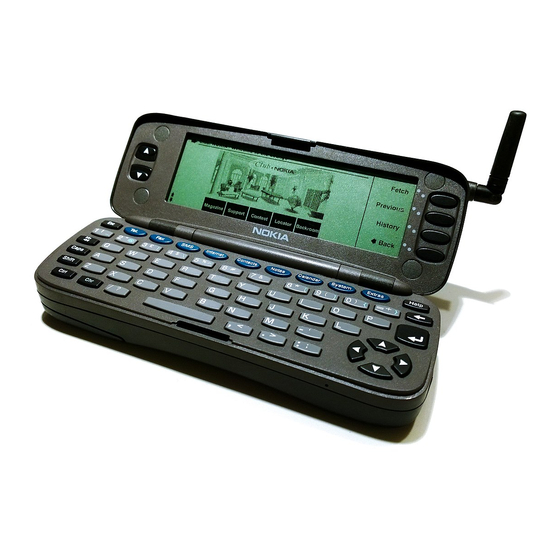
Overview Technical Documentation Figure 1. Basic Kit The NOKIA 9000 communicator integrates the functionality of the Nokia DTP–2 GSM/PCN data adapter card on its modified baseband and adds a second, improved user interface for data applications such as fax, terminal emulator, and graphical Internet browsers, e.g., World Wide Web (WWW). -
Page 16: Gsm/Pcn Networks
After Sales RAE/RAK–1N Overview Technical Documentation Figure 2. Personal Digital Assistant GSM/PCN Networks GSM is originally a pan–European digital cellular network standard, later phrased as the Global System for Mobile Communications. The standard is defined jointly by all related parties in the European Telecommunication Standard Institute (ETSI). -
Page 17: Modular Structure
PDA via a pair of cables. In addition the NOKIA 9000 has a dedicated attachable Li Ion battery and contains 2 cells with 730 mAh capacity (1Q/96) plus necessary protection circuitry with external connector. -
Page 18: Product Variants
Figure 3. Modular Structure Product Variants The NOKIA 9000 communicator has the type designator RAE/RAK–1N where RAE refers to the GSM version and RAK ,the PCN version. The table below shows the variants that apply to this product; these variations only affecting the QWERTY keymat layouts, illustrated in Figure 4 overleaf. -
Page 19: Figure 4. Pda Qwerty Keypads
After Sales RAE/RAK–1N Overview Technical Documentation SCANDINAVIAN GERMAN FRENCH Figure 4. PDA QWERTY keypads Page 1– 13 Original, 08/96... -
Page 20: Sales Packages
Overview Technical Documentation Sales Packages The NOKIA 9000 product family is a first generation GSM / PCN handportable. The family contains a basic sales package for portable use and optional accessories for office and mobile use. There is only one Nokia design version of the transceiver. - Page 21 After Sales RAE/RAK–1N Overview Technical Documentation Table 7. HF Car Installation Name of accessory Type code Material Notes code Power Cable PCH–4 0730009 External Audio Handset HSU–1 0640047 Swivel Kit MKR–1 0620033 Mounting Plate MKE–1 0650007 Installation Guide, CARK 60 9385069 HF Car Table 8.
-
Page 22: Technical Summary
After Sales RAE/RAK–1N Overview Technical Documentation Technical Summary The transceiver electronics consist of the following modules: – PDA (PIM & extended UI control), – Radio System (RF + System blocks), – UIF – SIM and audio submodule. The UIF Module is connected to the PDA module with a flex cable and a connector. - Page 23 After Sales RAE/RAK–1N Overview Technical Documentation Handset HF–Microphone Antenna Transceiver HSU–1 HFM–10 Battery RAK–1N (PCN) BLK–4S RAE–1N (GSM) HF–Speaker Cradle HFS–6 Antenna System connector connector Test battery BTD–1C System socket RS232 Charger connector PAR–1 connector Speaker conn. conn. IGNS HF Junction Box Desktop Charger HFJ–3 DCH–4...
-
Page 24: Mechanical Characteristics
After Sales RAE/RAK–1N Overview Technical Documentation Mechanical Characteristics Table 9. Mechanical Characteristics RAE–1 Dimensions Weight / g Volume/ cm Notes (WxLxH) / mm Transceiver 65*176*39 If antenna is in- with standard cluded, length battery pack is 189 Transceiver w/o same battery pack Radio module 57*170*16... -
Page 25: Vibration And Free Fall
USER‘S GUIDE that comes with the product. The transceiver is provided with a HELP system via both keypads (lid open/closed). Also, ‘on line’ help will be available on the Internet via the Nokia–club service. Page 1– 19 Original, 08/96... - Page 26 After Sales RAE/RAK–1N Overview Technical Documentation [This page intentionally left blank] Page 1– 20 Original, 08/96...
- Page 27 After Sales Technical Documentation RAE/RAK–1N Series Chapter 2 –Transceiver GE8/GE9– Baseband Block Original, 08/96...
- Page 28 After Sales RAE/RAK–1N Baseband Technical Documentation CONTENTS –Baseband Page No Introduction ............2–...
- Page 29 After Sales RAE/RAK–1N Baseband Technical Documentation Main components ......... . 2–...
- Page 30 After Sales RAE/RAK–1N Baseband Technical Documentation List of Figures Page No Figure 1. Interconnection diagram ....... . . 2–...
-
Page 31: Introduction
RF. All components are surface mounted. Transceiver GE8 is GSM; Tranceiver GE9 is PCN The connection to the NOKIA 9000 communicator PDA module is made using a board to board connector. The connections to the User Interface module (UIF) are made through the ‘passive’ PDA module. Besides the PDA board to board connector only the SIM/audio and battery connector are on the baseband module. -
Page 32: Figure 5. Interconnection Diagram
After Sales RAE/RAK–1N Baseband Technical Documentation The MCM 2 contains the 6 ICs in DSPU, AUDIO, ASIC and RFI submodules plus bypass capacitors and some resistors. The PWRU module is laid out in the CMT board using conventional SMD assembly. The rest of the functional modules are partly packaged in the MCM’s and partly SMD assembled on the CMT board. -
Page 33: Modes Of Operation
After Sales RAE/RAK–1N Baseband Technical Documentation Modes of Operation There are four different operation modes – active mode – idle mode – acting dead mode – power off mode Active Mode In the active state all circuits are powered and part of the module may be in idle mode. - Page 34 After Sales RAE/RAK–1N Baseband Technical Documentation Table 3. Supply Voltages and Power Consumption (continued) Pin / Conn. Line Symbol Minimum Typical / Maximum Unit / Notes Nominal 14 / B2B VCHAR 10.0V 12.0 13.0V Charger specifi- 31 / B2B cations, without load 4.5V 4.65V...
- Page 35 After Sales RAE/RAK–1N Baseband Technical Documentation 27 / B2B UIF(3:0) 0.7V Output/Input low keyboard 26 / B2B row lines/ 25 / B2B display 4.7V 4.85V 5.0V Output/Input high 24 / B2B data lines 28 / B2B UIF4 0.7V Output/Input low keyboard read/write strobe for...
- Page 36 After Sales RAE/RAK–1N Baseband Technical Documentation 6 / SIMFLEX SIMCLK 3.6V 4.85V 5.0V State ”1” Clock for SIM card 0.2V 0.7V State ”0” 7 / SIMFLEX SIMRESET 4.7V 4.85V 5.0V Output high Reset for SIM card 0.7V Output low 8 / SIMFLEX VSIM 4.7V 4.85V 5.0V...
-
Page 37: Ac Characteristics
After Sales RAE/RAK–1N Baseband Technical Documentation AC Characteristics Table 6. Audio Signals Pin / Type Line Symbol Minimum Typical / Maximum Unit / Notes Nominal 11 / SIM- MICN 5 mV 19 mV Differential FLEX MICP 12 / SIM- FLEX 3 / SIMFLEX EARN 124 mV... - Page 38 After Sales RAE/RAK–1N Baseband Technical Documentation Table 9. Personal HF microphone PHFMIC NOTES 1kHz rms MRP pressure +14 dBPa 50 cm from MIC MIC pressure –6 dBPa about 20 dB attenuation MIC output 3.1 mVrms mic sensitivity –64 dB (6.3 mV/Pa) 0 dB = 1V/uBar 1uBar=0.1Pa Codec gain 30.5 dB...
- Page 39 After Sales RAE/RAK–1N Baseband Technical Documentation Table 11. Accessory HS microphone (continued) HSMIC NOTES 1kHz rms Codec input level 12.5 mVrms Codec gain 26 dB Fixed 20 dB + programmable 0...22.5 dB Level –6 dBm0 / 250 mVrms 0 dBm0 = 490 mVrms Table 12.
-
Page 40: Connectors
After Sales RAE/RAK–1N Baseband Technical Documentation Table 14. Accessory HF speaker HFEAR NOTES 1 kHz rms Level –10 dBm0 / 620 0 dBm0 = 1965 mVrms mVrms Codec gain –16 dB nominal Output attenuation 6 dB 6 dB attenuation because of single ended output. Cable level 50 mVrms nominal minimum impedance 1kW... - Page 41 After Sales RAE/RAK–1N Baseband Technical Documentation Table 15. PDA board to board connector (B2B) (continued) Signal Name Pin(s) Notes DBUS received data from the accessories Transmitted DBUS–data to the accessories M2BUS Serial bidirectional data and control between the CMT and accessories. Cover switch state from PDA to CMT EXTMIC External audio input from accessories or...
-
Page 42: Connectors Out Of Transceiver Unit
After Sales RAE/RAK–1N Baseband Technical Documentation Connectors out of Transceiver Unit Table 18. Battery connector Signal Name Notes BGND Battery ground TBAT Battery temperature BTYPE Battery type Battery voltage Internal Signals and Connections Table 19. Signals Between RF and D2CA ASIC (MCM2) Signal Name Function Notes... -
Page 43: Circuit Descriptions
After Sales RAE/RAK–1N Baseband Technical Documentation Table 22. Signals Between RF and PWRU Signal Name Function Notes VREF Supply voltage for VCXO From PWRU to RF VBATT Battery voltage From PWRU to RF Ground Common ground Circuit Descriptions Power Distribution PSL+ VBATT VBATT... -
Page 44: Clocking Scheme
After Sales RAE/RAK–1N Baseband Technical Documentation Clocking scheme RF System Clock 26 MHz RFI Clock 13 MHz DSP Clock Sleep Mode: 60.2 MHz VCXO 135.4kHz differential sine wave enable OSCILLATOR ASIC AUDIO CODEC SIMCLK 3.25 / 1.625 MCU Clock 26 MHz Codec Sync Clock Codec Main Clock MCU Clock... -
Page 45: Reset And Power Control
After Sales RAE/RAK–1N Baseband Technical Documentation The DSP has its own crystal oscillator which can be turned off and on by the ASIC. The DSP uses differential sinusoidal clock. The frequency is 60.2 MHz. The MCU generates 8 kHz clock to the codec for the control data transfer. In the idle mode all the clocks can be stopped except 26 MHz main clock coming from the VCXO. -
Page 46: Watchdog System
After Sales RAE/RAK–1N Baseband Technical Documentation All devices are powered up at the same time by the PSL+. It supplies the reset to the ASIC at power up. The ASIC starts the clocks to the DSP and the MCU. After about 100 ms the PSL+ releases the reset to ASIC. ASIC releases the resets to MCU and RFI after 256 13 MHz clock cycles. -
Page 47: Ctrlu
After Sales RAE/RAK–1N Baseband Technical Documentation Failed operation: 4. ASIC resets MCU and DSP after about 0.5 s failure 5. PSL+ switches power off about 5 s after the previous XPWROFF pulse CTRLU Introduction The Control block contains a microcomputer unit (MCU) and five memory circuits (2xFLASH, 2xSRAM and EEPROM), a 20–bit address bus and a 16–bit data bus. - Page 48 After Sales RAE/RAK–1N Baseband Technical Documentation Table 23. External Signals and Connections, Inputs (continued) Signal Name Signal description From BTYPE Battery size identification Battery Conn JCONN Junction box connection identification AUDIO MBUSIN MBUS RX data B2B Conn Table 24. External Signals and Connections, Outputs Signal Name Signal description XPWROFF...
-
Page 49: Block Description
After Sales RAE/RAK–1N Baseband Technical Documentation Block description – MCU Memories The MCU has a 20 bits wide address bus A(19:0) and an 16–bit data bus with memories. The address bits A(19:13) are used for chip select decoding. The decoding is done inside the SCL in CTRLU submodule. Hitachi HD6475388 processor has internal ROM and RAM memories. - Page 50 After Sales RAE/RAK–1N Baseband Technical Documentation Table 27. Chip Select Generation A19 A18 A17 A16 A15 A14 A13 CHIP SELECT NOTES SRAM (page 1) 32K x 16 bit area SRAM (page 14) 28K x 16 bit area SRAM (page 14) SRAM (page 14) EEPROM (page 14) 8K x 8 bit area...
- Page 51 After Sales RAE/RAK–1N Baseband Technical Documentation – CTRLU – PWRU MCU controls the watchdog timer in PSL+. It sends a positive pulse at approximately 2 Hz to XPWROFF pin of the PSL+ to keep the power on. If MCU fails to deliver this pulse, the PSL+ will remove power from the system.
- Page 52 After Sales RAE/RAK–1N Baseband Technical Documentation – CTRLU – ACCESSORIES MBUS is used to control external accessories. This interface can also be used for factory testing and maintenance purposes. There are also some control and indication signals for the accessories: JCONN is used to indicate that junction box is connected.
- Page 53 After Sales RAE/RAK–1N Baseband Technical Documentation Table 29. External Signals and Connections, Inputs (continued) Signal Name Signal description From Charger on/off control CTRLU VCHAR Charging voltage B2B conn VOLTLIM Charging voltage limitation during call; affects HW voltage limit CTRLU Table 30. External Signals and Connections, Outputs Signal Name Signal description XRES...
- Page 54 After Sales RAE/RAK–1N Baseband Technical Documentation If the phone is in power–off state, the PSL+ will detect the charging voltage and turn on the phone. If the battery voltage is high enough the reset will be released and the MCU will start controlling charging. If the battery voltage is too low the phone stays in reset state and the charging control circuitry will pass small charging current to the battery.
- Page 55 After Sales RAE/RAK–1N Baseband Technical Documentation Main features of the DSP block: – speech processing – speech coding/decoding – RPE–LTP–LPC (regular pulse excitation long term prediction linear predictive coding) – voice activity detection (VAD) for discontinuous transmis- sion (DTX) – comfort noise generation during silence –...
- Page 56 After Sales RAE/RAK–1N Baseband Technical Documentation – frame structure control – control of operations during a TDMA frame (with ASIC) – control of multiframe structure – channel configuration control – data functions – RLP CRC calculation – fax V110 frame encode/decode –...
- Page 57 After Sales RAE/RAK–1N Baseband Technical Documentation Block description The DSPU communicates with the CTRLU through a mailbox in the D2CA ASIC. The software for the external memories are loaded through this mailbox in start up. The DSP includes two serial buses. One is used for digitized speech transfer between the DSP and the codec.
- Page 58 After Sales RAE/RAK–1N Baseband Technical Documentation AUDIO Introduction The AUDIO block contains an audio codec and a booster amplifier together with some peripheral components. The codec contains microphone and earpiece amplifiers and all the necessary switches for routing. The codec is controlled by the MCU. The PCM data comes from and goes to the DSP.
- Page 59 After Sales RAE/RAK–1N Baseband Technical Documentation Block description The codec has three microphone inputs and two earphone outputs. The microphone inputs from handportable and PHF microphones plus the external audio input can be therefore connected directly to the codec. The handportable earphone output and external audio are also connected directly to the codec using the two earphone output channels.
- Page 60 After Sales RAE/RAK–1N Baseband Technical Documentation The codec generates DTMF tones (key beeps) to the earphone and in PHF mode to the PHF speaker. When an external audio accessory is used, the DTMF tones are directed to the external audio output. In handportable and PHF modes the codec generates ringing tones and also some warning tones to the PHF speaker.
- Page 61 After Sales RAE/RAK–1N Baseband Technical Documentation Physically the D2CA ASIC is located in MCM2. The VCXO clock buffer and SIM power switch are assembled on CMT motherboard. Technical specification Table 36. External Signals and Connections, Inputs Signal Name Signal description From Logic supply voltage.
- Page 62 After Sales RAE/RAK–1N Baseband Technical Documentation Table 37. External Signals and Connections, Outputs (continued) Signal Name Signal description DSPCLKEN DSP clock circuit enable DSPU RFICLK RFI master clock (13 MHz) RFI2CLK RFI sleep clock (135.4 kHz) CODEC_CLK PCM data clock (512 kHz) DSPU, AU- PCMDATRCLKX Inverted PCM data clock (512 kHz)
- Page 63 After Sales RAE/RAK–1N Baseband Technical Documentation Interface to the MCU is done with 8 bit data bus, 5 bit lower address bus, 4 bit upper address bus, RSTROBEX, WSTROBEX, IRQX and NMI. ASIC is in the same memory space as MCU memories. There is also MBUS/RBUS detector and netfree counter on the ASIC.
- Page 64 After Sales RAE/RAK–1N Baseband Technical Documentation Coder is used to perform block encoding, decoding, and ciphering according to GSM algorithms A5 and A5/2. The ASIC takes care of the interface between the DSP and the RFI: TX modulator, RX filter, TX and RX sample buffers and controlling state machine.
- Page 65 After Sales RAE/RAK–1N Baseband Technical Documentation Table 40. External Signals and Connections, Outputs Signal Name Signal description Data acknowledge ASIC Automatic frequency control voltage TX transmit power control voltage / RX AGC voltage TXQP,TXQN differential TX quadrature signal TXIP,TXIN differential TX in–phase signal PDATA0 LNA gain reduction Table 41.
- Page 66 After Sales RAE/RAK–1N Baseband Technical Documentation [This page intentionally left blank] Page 2–40 Original, 08/96...
- Page 67 After Sales Technical Documentation RAE/RAK–1N Series Chapter 3 –Transceiver GE8/GE9 – RF Block Amendment 1 04/97...
- Page 68 After Sales RAE/RAK–1N Technical Documentation CONTENTS –RF Page No Introduction ............3–...
- Page 69 After Sales RAE/RAK–1N Technical Documentation Reference oscillator ........3–...
- Page 70 After Sales RAE/RAK–1N Technical Documentation List of Figures Page No Figure 1. GSM Frequency Map ........3–...
-
Page 71: Introduction
After Sales RAE/RAK–1N Technical Documentation Introduction The RF module for Responder is taken from the HD841 project with only minor modifications in the built–in and external antenna interfaces. Otherwise the circuitry and layout are almost completely the same as in HD841 GSM and PCN versions. -
Page 72: Main Technical Specifications
After Sales RAE/RAK–1N Technical Documentation Main Technical Specifications RF frequency plan 1st IF 2nd IF CRFRT 935–960 LO 1 LO 2 1006– 1031 890–915 VCXO: 26 MHz Figure 1. GSM Frequency Map 1805– 1st IF 2nd IF 3rd IF CRFRT 1880 1492–1567 LO 1... -
Page 73: Maximum Ratings
After Sales RAE/RAK–1N Technical Documentation Maximum Ratings The maximum battery voltage during the transmission should not exceed 8.5 V. Higher battery voltages may destroy the power amplifier. During charging this will be quaranteed by hardware based limiting which has maximum value 7.6 +/–0.3 V. However, the maximum voltage of the Li–Ion battery will be almost 8.5 V when the battery is full. - Page 74 After Sales RAE/RAK–1N Technical Documentation Battery 2 mA 7.2 V VCXO VREF (min. 5.7 V) Switch GSM: 1300 mA Power PCN: 900 mA Amplifier CRFCONT Vbias SYNTHPWR TXPWR RXPWR +4V5_TX: VHLO: VPLL: +4V5_RX: VTX: TX buffers VHF LO UMA1018 RF LNA CRFRT (VTX) Negat.volt.
-
Page 75: Control Signals
After Sales RAE/RAK–1N Technical Documentation Control Signals In the following tables (Table 2, 3, 4) the RF current consumption can be seen with different status of the control signals. The VCXO current is not included in the results. Table 2. Control Signals and Current Consumption GSM,PCN SYNTHPWR RXPWR... -
Page 76: Functional Description
After Sales RAE/RAK–1N Technical Documentation Functional Description Receiver The GSM receiver is a double conversion receiver. The PCN receiver has three conversions. The received RF signal from the antenna is fed via a duplex filter to the receiver unit. The signal is amplified by a discrete low noise preamplifier. The gain of the amplifier is controlled by the AGC control line (PDATA0). - Page 77 After Sales RAE/RAK–1N Technical Documentation Figure 4. RF Functional Block diagram Page 3– 11 Amendment 1 04/97...
-
Page 78: Frequency Synthesizers
After Sales RAE/RAK–1N Technical Documentation Frequency Synthesizers The stable frequency source for the synthesizers and base band circuits is discrete voltage controlled crystal oscillator (VCXO) in GSM and PCN.The frequency of the oscillators is controlled by an AFC voltage, which is generated by the base band circuits. The VCXO is always running when the CMT is powered up. -
Page 79: Rf Characteristics
After Sales RAE/RAK–1N Technical Documentation RF Characteristics Receiver Table 3. RF characteristics, Receiver Item RX frequency range , MHz 935 ... 960 1805 ... 1880 Type Linear, 2 IFs Linear, 3 IFs Intermediate frequencies , MHz 71 , 13 313, 87, 13 3 dB bandwidth ,kHz +/–... -
Page 80: First Mixer
After Sales RAE/RAK–1N Technical Documentation Table 4. Pre amplifier specifications Parameter Minimum Typical / Maximum Unit / Notes Nominal Frequency band 935–960 1805 – 1880 Supply voltage 4.27 4.73 Current consumption Insertion gain 16.5 Gain flatness +/– 0.5 Noise figure Reverse isolation Gain reduction IIP3... -
Page 81: First If Amplifier
After Sales RAE/RAK–1N Technical Documentation Parameter Minimum Typical / Maximum Unit / Notes Nominal IIP3 LO – RF isolation 15.0 LO power level First IF amplifier The first IF amplifier is a bipolar transistor amplifier. Table 6. 1st IF amplifier specification Parameter Minimum Typical /... -
Page 82: 2Nd Mixer (Only In Pcn)
After Sales RAE/RAK–1N Technical Documentation 2nd mixer (only in PCN) The 2nd mixer is a single balanced passive diode mixer. The local signal is balanced by a printed circuit transformer. The mixer down converts the 1st IF signal 313 MHz to 2nd IF signal 87 MHz. Table 7. -
Page 83: Receiver If Circuit, Rx Part Of Crfrt
After Sales RAE/RAK–1N Technical Documentation Receiver IF circuit, RX part of CRFRT The receiver part of CRFRT consists of an AGC amplifier of 57 dB gain, a mixer and a buffer amplifier for the last IF. The mixer of the circuit down converts the received signal to the last IF frequency. -
Page 84: Transmitter
After Sales RAE/RAK–1N Technical Documentation Transmitter Table 10. RF Characteristics, Transmitter Item TX frequency range 890...915 MHz 1710...1785 MHz Type Upconversion Upconversion Intermediate frequency 116 MHz 200 MHz Maximum output power 2 W (33 dBm) 1 W (30 dBm) Gain control range 20 dB 20 dB Maximum RMS phase error... -
Page 85: Upconversion Mixer
After Sales RAE/RAK–1N Technical Documentation Table 11. CRFRT TX–part specifications (continued) Modulator Inputs (I/Q) Minimum Typical / Maximum Unit / Notes Nominal Available linear RF power –10 dBm, ZiL=50 ohms Available saturated RF pow- –5 dBm, ZiL=50 ohms Total gain control range Gain control slope dB/V Suppression of 3rd order... -
Page 86: 1St Tx Buffer
After Sales RAE/RAK–1N Technical Documentation 1st TX buffer The TX buffer is a bipolar transistor amplifier. It amplifies the TX signal coming from the upconversion mixer. Table 12. 1st TX amplifier specification Parameter Minimum Typical / Maximum Unit / Notes Nominal Operating freq. -
Page 87: Power Amplifier
After Sales RAE/RAK–1N Technical Documentation Power amplifier The power amplifier is a three stage discrete amplifier. It amplifies the 0 dBm ( 2 dBm in PCN) TX signal to the desired output level. It has been specified for 5.5...8.5 volts operation. There are 5 x 330 mF capacitors in the near vicinity of the power amplifier to alleviate supply voltage degradation during TX burst. -
Page 88: Power Control Circuitry
After Sales RAE/RAK–1N Technical Documentation Power control circuitry The power control loop consists of a power detector and a differential control circuit. The power detector is a combination of a directional coupler and a diode rectifier. The differential control circuit compares the detected voltage and the control voltage (TXC) and controls voltage controlled amplifier (in CRFRT) or the power amplifier. -
Page 89: Vhf Pll
After Sales RAE/RAK–1N Technical Documentation Table 16. VCXO specification (continued) Parameter Minimum Typical / Maximum Unit / Notes Nominal Output voltage Vpp, sine wave for PLLs Harmonics –5 Control Voltage Range 0.25 4.45 Nominal Voltage for center frequency Control Sensitivity ppm/V Frequency stability, vs. -
Page 90: Uhf Pll
After Sales RAE/RAK–1N Technical Documentation Table 18. VHF VCO + buffer specification Parameter Minimum Typical / Maximum Unit / Notes Nominal Supply voltage Control voltage Supply current Operation frequency Output power level / 1 kohm Control voltage sensitivity MHz/V MHz/V Phase noise, GSM/PCN +/–... -
Page 91: Uhf Vco Buffers
After Sales RAE/RAK–1N Technical Documentation UHF VCO buffers The UHF VCO output signal is divided into the 1st mixer of the receiver and the upconversion mixer of the transmitter. The UHF VCO signal is amplified after division. There is one buffer for TX and one for RX. Table 20. -
Page 92: Connections
After Sales RAE/RAK–1N Technical Documentation Connections Antenna The default antenna in GSM transceiver is helix with turnable joint and in PCN a whip antenna with turnable joint also. The location of the antenna is in the gk2 module. The antenna signal is lead through the turnable hinge separating the gk2 and CMTmain modules using 50W flexible coaxial cable. - Page 93 After Sales Technical Documentation RAE/RAK–1N Series Chapter 4 –Transceiver GE8/GE9 – UIF Module...
- Page 94 After Sales RAE/RAK–1N Technical Documentation CONTENTS – User Interface Page No Introduction ............4–...
- Page 95 After Sales RAE/RAK–1N Technical Documentation List of Figures Page No Figure 1. LCDM – connections........4–...
- Page 96 After Sales RAE/RAK–1N Technical Documentation [This page intentionally left blank] Page 4– 4 Amendment 1 04/97...
-
Page 97: Introduction
After Sales RAE/RAK–1N Technical Documentation Introduction This document describe UIF (GK2 for GSM, GK2–1 for PCN) module. UIF module includes CMT display ,CMT keypad ,PDA soft keypad and antenna matching circuit with connectors. It has also connection to PDALCD (GK1). PDALCD and UIF modules, together these are called the LCDM. -
Page 98: Uif Flexes
After Sales RAE/RAK–1N Technical Documentation The major parts on the module assembly include the following: – CMT Display module. Same module as used in HD841 including LCD, Heat seal, LCD driver TAB circuit and Light guide. – CMT keydome assembly: Adhesive film holding 20 metal domes. –... -
Page 99: Uif Electronics
After Sales RAE/RAK–1N Technical Documentation Both flexes are made of flexible material. Flexible material is needed because the hinge will be opened thousands of times and the signals must be working all the time. UIF Electronics The following sections of circuitry are on the UIF module: –... - Page 100 After Sales RAE/RAK–1N Technical Documentation Table 2. DC characteristics of PDA Hinge–flex connector on LCDM module Pin / Line Symbol Mini- Typi- Maxi- Notes Type cal / Nomi- 10,17,24 / 6–3 / UIF LCMUIF(3:0) 0.7V Output/Input low keypad row lines/ row lines/ 4.65V 4.8V...
-
Page 101: Ac Characteristics
After Sales RAE/RAK–1N Technical Documentation Table 2. DC characteristics of PDA Hinge–flex connector on LCDM module (continued) Pin / Line Symbol Mini- Typi- Maxi- Notes Type cal / Nomi- 25 / 0.4 V Output low PDA LCD, PDALCD PDALCD Frame Frame 2.6 V Output high... - Page 102 After Sales RAE/RAK–1N Technical Documentation Table 4. Hinge flex connector (X001) signals (continued) Signal Name Signal description Note LCMUIF5 keypad row / LCD driver register select LCMUIF6 enable strobe for LCD driver Ground LCMCOL(3:0) 11–14 Keypad column write BACKLIGHTA Display and keypad illu- mination control LCMXPWRON CMT Power/Off key...
-
Page 103: Uif Mechanical Characteristics
After Sales RAE/RAK–1N Technical Documentation Table 6. RF Connectors Signal Name Connector Signal description Note X035 RF Signal to/from CMT module X040 RF Clips connector to/from An- tenna UIF Mechanical Characteristics Table 7. UIF Mechanical Characteristics feature value notes Weight Typical Dimensions 165.0x50.8x4.0mm... -
Page 104: Keypad And Display Illumination
After Sales RAE/RAK–1N Technical Documentation Keypad and display illumination The keypad illumination is achieved by using two transistors wired as simple constant current sinks. Each transistor supplies eight leds. The bases of the transistors are all wired together and supplied by emitter follower V40. -
Page 105: Antenna Matching Circuit
After Sales RAE/RAK–1N Technical Documentation Antenna matching circuit The purpose of the antenna matching circuit is to transform the antenna feedpoint impedance to 50 ohm, which is the nominal impedance of the antenna cable. The matching circuit consists of a series inductor and capasitor and shunt inductor in GSM and series inductor and shunt inductor in PCN. - Page 106 After Sales RAE/RAK–1N Technical Documentation [This page intentionally left blank] Page 4– 14 Amendment 1 04/97...
- Page 107 After Sales Technical Documentation RAE/RAK–1N Series Chapter 5 – Transceiver GE8/GE9 – SIM Flex Module Original, 08/96...
- Page 108 After Sales RAE/RAK–1N SIM Flex Technical Documentation CONTENTS – SIM flex Page No Introduction ............5–...
- Page 109 After Sales RAE/RAK–1N SIM Flex Technical Documentation Introduction The purpose of the SIM–flex is basically to connect ancillary parts to the CMT. It has no active electronics and the main parts are the audio components, mic, low profile buzzer and speaker plus a SIM–connector. Flex Connector EMC–tape &...
- Page 110 After Sales RAE/RAK–1N SIM Flex Technical Documentation Table 2. Digital Control Signals Pin/ Line Symbol Mini- Typi- Maxi- Notes Connec- cal / Nomi- nal (1) 2 / SIM BUZZ2 0.7V Input low, buzzer on 5.5V 7.2V 8.4V Input high, buzzer 6 / SIM SIMCLK 3.6V...
- Page 111 After Sales RAE/RAK–1N SIM Flex Technical Documentation AC Characteristics Table 5. Audio Signals Pin / Line Symbol Minimum Typical / Maximum Unit / Notes Connector Nominal 12 / SIM MICP 5 mV 19 mV Differential 11 / SIM MICN 3 / SIM EARN 124 mV 1.965 V...
- Page 112 After Sales RAE/RAK–1N SIM Flex Technical Documentation [This page intentionally left blank] Original, 08/96 Page 5–6...
- Page 113 After Sales Technical Documentation RAE/RAK–1N Series Chapter 6 PDA Hardware Module GP1 Original, 08/96...
- Page 114 After Sales RAE/RAK–1N PDA Hardware Technical Documentation CONTENTS – PDA unit Page No Introduction ............6–...
- Page 115 After Sales RAE/RAK–1N PDA Hardware Technical Documentation List of Figures Page No Figure 1. PDA Interconnection diagram ......6–...
- Page 116 After Sales RAE/RAK–1N PDA Hardware Technical Documentation [This page intentionally left blank] Page 6 – 4 Original, 08/96...
-
Page 117: Introduction
RAE/RAK–1N PDA Hardware Technical Documentation Introduction This chapter describes the PDA system hardware used in the NOKIA 9000 communicator. The PDA module is used to run all applications that utilise the bigger (640x200) LCD screen. Technical Summary Table 1. List of functional blocks on PDA module... -
Page 118: Modes Of Operation
After Sales RAE/RAK–1N PDA Hardware Technical Documentation CMT Module CMT Module SA20:1, D15:0 MA9:0,D15:0 MBUS Audio PROCU 1M x 16 1M x 16 1M x 16 1M x 16 FLASH FLASH FLASH DRAM Control PDAPWRU MA 9:0/SA20:1 LCDM module DBUS PDALCD LCD, Testpads... -
Page 119: Dc Characteristics
After Sales RAE/RAK–1N PDA Hardware Technical Documentation DC Characteristics Table 2. Supply Voltages and Power Consumption Line Symbol Minimum Typical / Maximum Unit / Notes Nominal 5.75V 7.2V CMT Software limit 5.5V 7.2V 8.7 +/– 0.3V CMT Hardware limit 5.5V 7.2V 7.6 +/–... - Page 120 After Sales RAE/RAK–1N PDA Hardware Technical Documentation Table 3. DC characteristics of board to board connector Signals Pin / Line Symbol Mini- Typi- Maxi- Notes Type. cal / Nomi- nal (1) 6 / UIF BACKLIGHT 0.7V Output low, back- Display lights off and key- pad illu...
- Page 121 After Sales RAE/RAK–1N PDA Hardware Technical Documentation Pin / Line Symbol Mini- Typi- Maxi- Notes Type. cal / Nomi- nal (1) 29 / UIF UIF5 0.7V Output/Input low keypad LCD driver LCD driver 4.7V 4.85V 5.0V Output/Input high register select 30 / UIF UIF6 0.7V...
- Page 122 After Sales RAE/RAK–1N PDA Hardware Technical Documentation Table 4. DC characteristics of system connector signals Line Symbol Mini- Typi- Maxi- Notes cal / Nomi- VCHARGER 13.0 Isink < 730mA Charger voltage 730m 800mA 870m Uin < 10V 0.7V Input low level SYSMBUS Isink<5mA- Baud rate...
- Page 123 After Sales RAE/RAK–1N PDA Hardware Technical Documentation Line Symbol Mini- Typi- Maxi- Notes cal / Nomi- E103 JTAGTDO 2.735 State ”1” JTAG data 0.4V State ”0” E104 MBUS 0.7V Input low level Isink<5mA- Baud rate 3.0V 5.0V Input high level 9600 bits/ 9600 bits/ 0.2V...
- Page 124 After Sales RAE/RAK–1N PDA Hardware Technical Documentation Table 6. DC characteristics of LCDM flex connector on PDA module Pin / Line Symbol Mini- Typi- Maxi- Notes Type cal / Nomi- 6–3 / UIF LCMUIF(3:0) 0.7V Output/Input low keypad row lines/ display 4.65V 4.95V...
-
Page 125: Ac Characteristics
After Sales RAE/RAK–1N PDA Hardware Technical Documentation Table 6. DC characteristics of LCDM flex connector on PDA module (continued) Pin / Line Symbol Mini- Typi- Maxi- Notes Type cal / Nomi- 25 / 0.4 V Output low PDALCD LCD, Frame 2.735 V Output high Pulse... -
Page 126: Connectors Inside Transceiver Unit
After Sales RAE/RAK–1N PDA Hardware Technical Documentation Connectors Connectors Inside Transceiver Unit Table 8. PDA board to board connector Signal Name Notes 1, 44 Battery voltage 2, 5, 7, 10, 13, Ground 21, 22, 23, 37, 39, 40 PHFMICN PHF microphone (negative node) PHFMICP PHF microphone (positive node) BACKLIGHT... - Page 127 After Sales RAE/RAK–1N PDA Hardware Technical Documentation Table 8. PDA board to board connector (continued) Signal Name Notes EXTMIC External audio input from accessories or handsfree microphone. Multiplexed with junc- tion box connection indication. 16.8k pull down in CMT EXTEAR External audio output to accessories or hands- free speaker.
-
Page 128: Connectors Out Of Transceiver Unit
After Sales RAE/RAK–1N PDA Hardware Technical Documentation Connectors Out of Transceiver Unit Table 11. System Connector Signal Name Notes VCHARGER 1, 2 Battery charging voltage. SYSMBUS Serial bidirectional data and control between the handphone and accessories. TESTMODEX Test SW activation SYSEXTMIC External audio input from accessories or handsfree microphone. -
Page 129: Internal Signals And Connections
After Sales RAE/RAK–1N PDA Hardware Technical Documentation Internal Signals and Connections Table 13. Signals Between PROCU and power supply unit Signal Name Function Notes LCDPWM PWM signal for LCD voltage control LCD contrast control LCDVCCON LCD Vcc on/off LCDVEEON LCD Vee on/off PWRGOOD Reset signal for CPU VSYS valid... -
Page 130: Functional Description
After Sales RAE/RAK–1N PDA Hardware Technical Documentation Functional Description Introduction Intel E3G is 386 based core with all needed peripherals on same chip. E3G is used to execute all applications, GEOS, DOS, BIOS, and TFFS. Clocking Scheme Actual clock signals are not routed to any other chip than previously mentioned E3G. -
Page 131: Pda Power Management Principle
After Sales RAE/RAK–1N PDA Hardware Technical Documentation PDA power management principle. Operating voltage is always ON on the PDA module when battery is connected and charge level on the battery is above PDA power supply limit (HW cutt–off). When battery is connected voltage must rise over ’PDA HW limit cancel voltage’... -
Page 132: Cmt Power Management Principle
After Sales RAE/RAK–1N PDA Hardware Technical Documentation CMT power management principle. The goal is that existing power management scheme of CMT in HD841 is changed as little as possible. CMT module has power switch that works as on normal DCT1 cellular phones. The CMT_PDA_REQUEST_SERVICE state is implemented to support requests from PDA even when CMT is switched off. -
Page 133: Battery Charge Level Limits On Cmt And Pda
After Sales RAE/RAK–1N PDA Hardware Technical Documentation Battery charge level limits on CMT and PDA Figure 5 (overleaf) shows an example of combined CMT and PDA critical battery levels, measurement accuracy (+/– 50mV). There are two kind of limits most of which are implemented in software. The AD converter, located in the CMT module, is used as a source for battery level values needed by both CMT and PDA software. - Page 134 After Sales RAE/RAK–1N PDA Hardware Technical Documentation Battery low level warning 1 6.2V CMT battery cut–off 5.75V Battery low level warning 2 5.5V CMT HW limit PDA limit (Data save) 5.0V PDA HW cut–off Battery protect circuit 4.0 –4.4V cut–off Figure 5.
-
Page 135: Emiu
After Sales RAE/RAK–1N PDA Hardware Technical Documentation EMIU This module contains only passive components to suppress EMI generated voltages on external signal lines. Note 1. B2B = Board to board connector between PDA and CMT modules Table 14. External Signals and Connections, Inputs Signal Name Signal description From (1) - Page 136 After Sales RAE/RAK–1N PDA Hardware Technical Documentation Note 2. MICCON = Hands–free microfone connector on PDA module Note 3. SC = System Connector Table 15. External Signals and Connections, Outputs Signal Name Signal description To (1,2,3) BACKLIGHTO Backlights on/off (control) LCDMCON / BACKLIGH- KEYDO(2:0)
-
Page 137: Procu
After Sales RAE/RAK–1N PDA Hardware Technical Documentation PROCU The Processing unit contains integrated Intel E3G CPU (CPU and peripherals on the same chip), two types of memory circuits (DRAM, FLASH), a 22–bit address bus (26 bit internally), and a 16–bit data bus. PROCU functions: –... -
Page 138: Block Description
After Sales RAE/RAK–1N PDA Hardware Technical Documentation Table 17. External Signals and Connections, Outputs (continued) Signal Name Signal description 5VPDX 5V regulator powerdown PDAPWRU XPWRON Power key (active low) B2B / XPOWER- LCMCON / LCMXPOW- ERON RBUSRXD RBUS receive of CMT (CMT <– PDA) B2B / RBUSRXD RSTXD... -
Page 139: Memory Map
After Sales RAE/RAK–1N PDA Hardware Technical Documentation DRAM area is composed of a single 1M x 16 bit chip. The access time of 70 ns enables zero wait–state page access and one wait–state page fault. FLASH memory is used for two purposes on this device. Two 1M x 16 bit chips (75 ns) are used for BIOS, DOS, GEOS and applications this memory is usually called XIP FLASH. - Page 140 After Sales RAE/RAK–1N PDA Hardware Technical Documentation Table 18. (continued) Memory Map 0B8000 EMS page 2 (XIP page 1) 0B2BFFF EMS register 0BC000 EMS page 3 (Fixed GEOS XIP) 0BFFFF EMS register 0C0000 GEOS XIP (XIP FLASH 1.) 0ECBFF Double mapped area 0ECC00 ROM–DOS (XIP FLASH 1.) 0F77FF...
- Page 141 After Sales RAE/RAK–1N PDA Hardware Technical Documentation Table 18. (continued) Memory Map DOS ROM–DISK about 80k 3F00000 GEOS and applications (XIP FLASH 1) 3FFFBFF Upper non–resident XIP 3FFFC00 Reserved for manufacturing and aftersales data 3FFFF9F 3FFFFA0 PDA_PROD_HW_VERSION 3FFFFAF 3FFFFB0 PDA_PROD_HW_CODE 3FFFFBF 3FFFFC0 PDA_PROD_HW_NUMBER...
- Page 142 After Sales RAE/RAK–1N PDA Hardware Technical Documentation 100000h     BIOS BIOS 16 kbytes     True FFS True FFS 20 kbytes F0000h     DOS area, 43 K. ROM–DOS resides here full time. E0000h Â...
- Page 143 After Sales RAE/RAK–1N PDA Hardware Technical Documentation 250000h 240000h 230000h 220000h 210000h 200000h É É É É É É É É É É 1F0000h É É É É É 1E0000h É É É É É É É É É É 1D0000h É...
- Page 144 After Sales RAE/RAK–1N PDA Hardware Technical Documentation Jump to BIOS code, Manufacturing and 4000000h Aftersales data 3FFFC00 GEOS and Applications (non–resident XIP), DOS ROM_DISK 3F00000h BIOS 16K, TFFS 20K, DOS 43K, GEOS XIP 3EC0000h 177K + 16K 2 Mbytes (XIP FLASH 1.) 3E00000h GEOS and Applica- tions...
- Page 145 After Sales RAE/RAK–1N PDA Hardware Technical Documentation – Chip selects E3G CPU has four programmable chip selects. Size of the memory block can be defined with 2K resolution. Start address can be changed in 2K boundaries. These chip selects have independent programmable wait states (0–64).
-
Page 146: I/O Usage On E3G Cpu
After Sales RAE/RAK–1N PDA Hardware Technical Documentation RS232 FLASH load can be done with standard PC with a serial port and FLASH loading software. Upload is also possible with this software. On the PDA module RS232 FLASH download software is part of the BIOS. RS232 FLASH download commands are integrated to maintenance software. -
Page 147: I/O Map
After Sales RAE/RAK–1N PDA Hardware Technical Documentation Table 20. I/O usage on E3G CPU Signal name E3G CPU pin Polarity Reset value PWRGOOD RESET# H = Power good – (In) 5VPDX PMI2 / P45 L = Shut down TESTMODEX (Input) DTR0# / P02 L = Test mode –... -
Page 148: Interrupt Map
After Sales RAE/RAK–1N PDA Hardware Technical Documentation Table 21. I/O Map (continued) Device Address Note Chip Select Unit F400h – F463h E3G Specific E3G Clock Unit F800h, F87Bh E3G Specific E3G Bus Control Unit F810h – F813h E3G Specific E3G Chip Configuration Regis- F820h –... - Page 149 After Sales RAE/RAK–1N PDA Hardware Technical Documentation Main components – E3G CPU 80386 based CPU. Static design. Using external clock source maximum clock rate 33MHz. With internal PLL’s 23.96MHz. All needed peripherals are integrated to the same chip. Peripherals are as follows: –...
- Page 150 After Sales RAE/RAK–1N PDA Hardware Technical Documentation – 1M*16bit FLASH memory 120 ns – Intel 28F016SV 070 – 120 ns maximum read access time – SMART voltage device with 5 Volt programming – Used to store application data under FLASH File System –...
- Page 151 After Sales RAE/RAK–1N PDA Hardware Technical Documentation PDAPWRU Technical Description The power block creates supply voltages for the PROCU and LCDM, generates reset signal for CPU and contains LCD contrast control and enable circuits. Input filter is required to reduce input noise of switching regulators.
- Page 152 After Sales RAE/RAK–1N PDA Hardware Technical Documentation Table 24. External Signals and Connections, Outputs Signal Name Signal description To (1) VSYS System voltage 3.3V PROCU, SIRU VCC5 5V for FLASH and RBUS PROCU PWRGOOD Reset signal for CPU PROCU VBACK Backup battery voltage to RTC PROCU LCDVCC...
- Page 153 After Sales RAE/RAK–1N PDA Hardware Technical Documentation Table 25. Electrical characteristics (continued) Parameter Mini- Typi- Max- Units Notes/conditions VCC5 4.825 5.175 tolerance over temperature and load range dropout voltage at I=50mA regulator I =50mA peak current 100mA ground pin current (supply current) 3.04 3.08 3.11...
- Page 154 After Sales RAE/RAK–1N PDA Hardware Technical Documentation The controller has internal 1.23V bandgap reference and soft start circuitry for power–up. Overcurrent comparator disconnects the controller in short circuit conditions. After this soft start cycle is made in power–up. Output ripple voltage is determined by output capacitor ESR value which is minimized to reduce EMI.
- Page 155 After Sales RAE/RAK–1N PDA Hardware Technical Documentation VCC5 regulator 5V output is used only for data writing to FLASH memory and RBUS signals. Regulator is taken out of shutdown when it is needed. This simple linear regulator has pnp control transistor and overcurrent/overtemperature protection circuitry.
- Page 156 After Sales RAE/RAK–1N PDA Hardware Technical Documentation Main components – 3.3V current mode PWM controller IC – MAX763AESA from Maxim – 5V linear regulator – LP29801M5–5.0 from National Semiconductor – 21V switch mode PFM controller IC – MAX772ESA from Maxim –...
- Page 157 After Sales RAE/RAK–1N PDA Hardware Technical Documentation SIRU Introduction IrDA transceiver and RS232 buffer are located to this module. Infrared interface conforms to the Infrared Data Association Serial Interface (SIR) Physical Layer LInk Specification. SIRU functions: – external interface signalling (IrDA and RS232) Technical Description Table 26.
- Page 158 After Sales RAE/RAK–1N PDA Hardware Technical Documentation [This page intentionally left blank] Page 6 – 46 Original, 08/96...
- Page 159 After Sales Technical Documentation RAE/RAK–1N Series Chapter 7 Service Software Amendment 1 04/97...
- Page 160 After Sales RAE/RAK–1N Service Software Technical Documentation CONTENTS – Service Software Page No Introduction ............7–...
- Page 161 After Sales RAE/RAK–1N Service Software Technical Documentation 3.3.1 – TX Power Level ........7–...
- Page 162 After Sales RAE/RAK–1N Service Software Technical Documentation 2.2 – Test Buzzer ......... . 7–...
- Page 163 After Sales RAE/RAK–1N Service Software Technical Documentation Flash Downloading ..........7–...
- Page 164 After Sales RAE/RAK–1N Service Software Technical Documentation List of Figures Page No Figure 1. Dongle insertion ........7–...
- Page 165 Technical Documentation Introduction The Nokia 9000 service software is a dual purpose package designed to test all CMT and PDA functions by means of menu driven user interfaces; it is also used to download new flash images. The software requires that a dongle, PKD–1 , be fitted to the PC parallel in order to enable software...
- Page 166 After Sales RAE/RAK–1N Service Software Technical Documentation Testing Functions Mechanical Connections Caution: Make sure that you have switched off the PC and the printer before making connections ! Do not connect the PKD–1 key to the serial port. You may damage your PKD–1 ! Attach the protection key PKD–1 to parallel port one (25–pin female D–connector) of the PC.
- Page 167 After Sales RAE/RAK–1N Service Software Technical Documentation Minimum mode switch PAS–1 Dummy Battery – to power COM1 COM2 LPT–1 Supply DAU–2/2T PKD–1 DLR–1 Figure 2. Servicing setup Loading the Software The program is delivered on a diskette and can also be installed on the hard disk, which is recommendable to obtain maximum data access rate.
- Page 168 After Sales RAE/RAK–1N Service Software Technical Documentation Complete Menu Structure PC Setup 1 Load New Setup 2 Save Current Setup CMT Testing and Adjustments 1 RF Controls 2 Adjustments 3 Call Simulation 4 Internal Audio Loop 5 External Audio Loop 6 Logic Controls 7 Run MCU Selftests 8 Set MCU Start–Up Self–tests...
- Page 169 After Sales RAE/RAK–1N Service Software Technical Documentation CMT Menu Structure –Testing and Adjustment RF Controls 1 Actie Unit (TX/RX)......: RX 2 TX Power Level........: 15 3 Operation Mode (Burst/Continuous).: Burst 4 TX Data Type (0/1/RND).....:..1 5 Continuous Mode Channel....: 60 6 Channel..........: 60 7 Monitoring Channel......: 1 8 AGC..........: 81...
-
Page 170: Using Menus
After Sales RAE/RAK–1N Service Software Technical Documentation CMT Menu Structure – ME Short Code Memory User Setting and Values 1 Lock ID....35317 2 Master Code . - Page 171 After Sales RAE/RAK–1N Service Software Technical Documentation Help Functions The help key <F1> can be used anytime when a menu is on the display. The help key is context–sensitive and gives information according to which function is highlighted. The <Esc> key closes the help window.. Text Editing Windows When you have made a selection which needs some additional information, the basic text editing window is activated.
- Page 172 After Sales RAE/RAK–1N Service Software Technical Documentation When the insert mode is activated the <Back space> key moves the cursor back and deletes the character under the cursor so that all characters after the deleted character are moved one position back. If the cursor is at the first position of the first line nothing happens.
- Page 173 After Sales RAE/RAK–1N Service Software Technical Documentation CMT Menu Commands When you start the program, the phone will initialise if correctly connected. It not an error message will appear. Once initialised, the main menu can be seen on the screen; there are nine main functions; The phone defaults to ‘Normal’...
- Page 174 After Sales RAE/RAK–1N Service Software Technical Documentation 1 – PC Setup When Save Current Setup is selected the program asks for a setup file name. The saved information will include all parameters shown below: Command line parameter value for COM–port selection –...
- Page 175 After Sales RAE/RAK–1N Service Software Technical Documentation input (Start value = Int) output (Start value = Int) loop (Start value = Off) – External audio loop: interface (Start value = HS) – Logic controls LCD Test Display (Start value = 1) Load New Setup –...
- Page 176 After Sales RAE/RAK–1N Service Software Technical Documentation 3 – Testing and Adjustments When testing and adjustment menu is selected, the phone mode must be set to the ‘Local’ value. If the local mode is not set, an error message is shown.
- Page 177 After Sales RAE/RAK–1N Service Software Technical Documentation PCN Version RF Control Information Window When RF controls menu is activated, the information window is generated and updated when information is changed. This window closes when exiting the RF controls menu. The next table shows the information window display on different situations: Active Unit = TX Operation mode =...
- Page 178 After Sales RAE/RAK–1N Service Software Technical Documentation 3.1.1 – Active Unit Either receiving or transmission tests can be selected. When TX is selected, Data transmission is activated : DIf operation mode is continuous, – Continuous mode is changed to burst mode, DIf operation mode is burst, –...
- Page 179 After Sales RAE/RAK–1N Service Software Technical Documentation 3.1.3 – Operation Mode When burst selection is used, – synthesizer is controlled by using GSM/PCN receiving/transmission /measuring synthesizer control sequence – synthesizer channel numbers are as given with Channel/Monitoring Channel selections – if Active Unit is TX, data (selected with TX Data Type) is sent and the TX power is connected When continuous selection is used, –...
- Page 180 After Sales RAE/RAK–1N Service Software Technical Documentation 3.2 – Adjustments All adjustments which have EEPROM saving selection have the next kind of behaving with F2 and ESC keys. When adjustment function is activated and <F2> key is used the program will ask are the values saved to the EEPROM or not.
- Page 181 After Sales RAE/RAK–1N Service Software Technical Documentation 3.2.2 – TX Power Tuning Once selected the display asks the following: Note: Base Power level activated unless command is interrupted by ESC Do you want to load Values from EEPROM? (Y/N) _ If <Y>...
- Page 182 After Sales RAE/RAK–1N Service Software Technical Documentation There is one selection which is used for power coefficient calculation. Only three power coefficients (biggest, third smallest and smallest) are needed for tuning, the rest are calculated. The calculation is activated with <F3> key. The power coefficients which are calculated from the tuned coefficients are displayed on the different columns than the others.
- Page 183 After Sales RAE/RAK–1N Service Software Technical Documentation If the power tuning function is ended and EEPROM values are not received or an EEPROM fault is noticed, an error message is shown. Error message asks to initialize the phone and if initialization is performed successfully the program is restarted.
- Page 184 After Sales RAE/RAK–1N Service Software Technical Documentation The next menu is displayed after the answer. When a selection is made, the menu will disappear from the display and the control will be on the tuning window. The right top hand corner of the tuning window shows which tuning is activated.
- Page 185 After Sales RAE/RAK–1N Service Software Technical Documentation Tune Amplitude Difference When this selection is made the user can increase or decrease the amplitude difference within 0.1 dB steps. The current amplitude difference is shown on the tuning window with numbers and a bar figure. Tune Phase Difference: When this selection is made the user can increase or decrease the phase difference within 0.5 steps.
- Page 186 After Sales RAE/RAK–1N Service Software Technical Documentation 3.2.4 – RSSI Calibration When function is activated the selected channel is checked. If none of the receiving channel numbers from 50 to 70 in GSM mode and 670 to 730 in PCN mode is selected then an error message is shown and the user is asked to change the channel to the valid receiving channel area.
- Page 187 After Sales RAE/RAK–1N Service Software Technical Documentation Upon exiting, the next selections are set to the values which were selected before this adjustment. – Active Unit – Operation Mode 3.2.5 – AFC Diagram The following automatic selections are made when this tuning function is activated: –...
- Page 188 After Sales RAE/RAK–1N Service Software Technical Documentation 3.2.6 – Noise Sensitivity This function is used for making Signal to Noise measurement. The following automatic selections are made when this tuning function is activated: – Active Unit = RX – Operation mode = Continuous –...
- Page 189 After Sales RAE/RAK–1N Service Software Technical Documentation When signal data is received, the distance to clipping signal level is shown as dBs on the display. When either signal or noise measurement results are received ”MEASURING” text is removed and the first mentioned help line is on the display.
- Page 190 After Sales RAE/RAK–1N Service Software Technical Documentation If no measurement result is received when <Esc> key is used, the information message is shown. The user can remove the information message with <Y>, <N> or <Esc> key. The measurement will be terminated by using <Y>...
- Page 191 After Sales RAE/RAK–1N Service Software Technical Documentation 3.3 – Call Simulation 3.3.1 – TX Power Level All power levels (GSM: 5...15 PCN: 0...10) can be selected. This updates the same parameter as TX Power Level in the RF Controls menu. Note that TEST value cannot be selected.
- Page 192 After Sales RAE/RAK–1N Service Software Technical Documentation 3.4 – Internal Audio Loop This test interface allows selection of input and output (Internal / External / Phf) and also connects and disconnects the test loop. The sent audio signal level has a constant value which depends on the selected interfaces.
- Page 193 After Sales RAE/RAK–1N Service Software Technical Documentation When Make a Measurement is selected, the received signal strength is displayed (square root of the received value) on the separate window. If any of the signal values differs more than 3 dB from the reference values shown in the table below, the OUT OF RANGE message will be displayed.
- Page 194 After Sales RAE/RAK–1N Service Software Technical Documentation 3.6.1 – Read A/D Converters After this selection new window is shown: No value is shown when selected. When correspondent messages are received, the A/D converter values (10 bits decimal numbers) are displayed and read again. The exit is made with <Esc>. 3.6.3 –...
- Page 195 After Sales RAE/RAK–1N Service Software Technical Documentation 3.7 – MCU Selftests When this selection is used, the user is informed The phone will be set to the minimum mode Y will run the special test mode and a reset will occur making MCU SW run only inside the MCU ROM code (=minimum mode).
- Page 196 After Sales RAE/RAK–1N Service Software Technical Documentation 3.8 – Set MCU Start–up Self–tests This menu is used for changing the state of the EEPROM selectable tests. When selection is ”On”, the test will be run every time when automatic start–up self–tests are activated (e.g. in power–up). When menu is selected, the previous values will be read from the MCU EEPROM and shown on the screen.
- Page 197 After Sales RAE/RAK–1N Service Software Technical Documentation 4 – ME Memory Functions When ME Memory functions menu is selected the Phone Mode must be set to ‘Local’. If the local mode is not set, an error message is shown. Different parameters saved to the memory of ME can be read from memory or written to the memory.
- Page 198 After Sales RAE/RAK–1N Service Software Technical Documentation 4.1.1 – Lock ID When this function is activated, the code can be edited; note that code is saved to the ME memory together with other user settings and values. Only digits are accepted for Security lock. 4.1.2 –...
- Page 199 After Sales RAE/RAK–1N Service Software Technical Documentation 4.3 – Write HW Version When HW version is selected, the current version is read from the phone and displayed. 4.4 – IMEI Edit When this selection is made, the old IMEI is requested from EEPROM. If IMEI is not received within 2 seconds (approx.), an error message is displayed .
- Page 200 After Sales RAE/RAK–1N Service Software Technical Documentation 4.6 – Set UI factory Values This function sets the UI parameters to factory default values. Phone mode must be in the Local mode when this menu is selected. 4.7 – Set Factory Values The selection sets all except IMEI factory values (including UI).
- Page 201 After Sales RAE/RAK–1N Service Software Technical Documentation 6. SW and HW Versions This menu shows the current software and hardware versions. GSM Version PCN version Page 7– 43 Amendment 1 04/97...
- Page 202 After Sales RAE/RAK–1N Service Software Technical Documentation The next tuning window will be activated automatically after value selection. The power is presented in GSM values (5...15). The base GSM power (5) is selected automatically when the function is started. The test value is always the same when the function is started for the first time.
- Page 203 After Sales RAE/RAK–1N Service Software Technical Documentation 7 – Phone Mode With this function you can change the phone state (Normal or local mode). When Normal mode is selected the normal start up functions take place in the phone and the phone is in normal operating mode. When the local mode is selected the phone is deactivated to enable e.g.
- Page 204 After Sales RAE/RAK–1N Service Software Technical Documentation 9 – Faultlog Faultlogger allows a complete service record to be built up from each phone repaired. The software automatically read the products details from EEPROM and writes a record to a pre–determined file. When an engineer adds the repair information, a complete service record is formed and this record can then be utilsed by database software for accurate fault reporting purposes...
- Page 205 After Sales RAE/RAK–1N Service Software Technical Documentation PDA Menu Commands Introduction Upon selection, the service software will try to establish a communications link to the PDA module via the second serial port (if fitted) or alternatively when the DLR–1 connector is attached to the first serial port in place of the MBUS.
- Page 206 After Sales RAE/RAK–1N Service Software Technical Documentation At this point re–connect the power supply and a ‘Target responding’ message should be displayed as shown below. NOTE This procedure is necessary in order for Pinging to function correctly. If the default ’None’ is chosen, only the ’Flash Utilities,’Flash Several Targets’ and ’JTAG Flashing’...
- Page 207 After Sales RAE/RAK–1N Service Software Technical Documentation 1.– Initialisation This menu provides functions to direct the target either to the BIOS or to the DOS– testmode. The speed of the communications channel may be changed and verification of communications channel validity is also possible.
- Page 208 After Sales RAE/RAK–1N Service Software Technical Documentation Note: Any user options become highlighted once the menu item is selected, these can be changed by using the arrow keys 1.2 – Set Serial Speed This menu item provides means to change the speed of the serial channel used between the service software and the PDA.
- Page 209 After Sales RAE/RAK–1N Service Software Technical Documentation 2 – Test Peripherals This menu provides functions to test the discrete components of the PDA target. 2.1 – Test LCD Panel This menu provides tests for the PDA LCD panel. Various test patterns can be chosen to be displayed with any contrast value.
- Page 210 After Sales RAE/RAK–1N Service Software Technical Documentation 2.3 – Test Power Management Inputs This menu provides a test for the PDA power management inputs. The enquired input parameters from the user are: TimeOut default: 5.0s range: 0.1 – 25.5s The input parameters are given as plain figures without units. Time referred input values are given as hundreds of milliseconds.
- Page 211 After Sales RAE/RAK–1N Service Software Technical Documentation If the Mode is set to Input, the target is commanded to wait for the Output Byte from the tranceiver connected to the service software. If the Output byte is received in the target, the test is considered successful. 2.6 –...
- Page 212 After Sales RAE/RAK–1N Service Software Technical Documentation 4 – DRAM Utilities This menu provides functions to access the PDA DRAM. 4.1 – Test DRAM This menu provides a test utility for testing the PDA DRAM. User options are: Test type default: WalkingBit Range: WalkingBit...
- Page 213 After Sales RAE/RAK–1N Service Software Technical Documentation 4.3 – Write DRAM This menu provides means to write the DRAM of the target. User options are: Start Address default: 000000h Range: 000000 – 1FFFFFh Bytes default: none Range: 0 – FFh Note: The number of bytes has to be even 5 –...
- Page 214 After Sales RAE/RAK–1N Service Software Technical Documentation 5.3 – Write I/O Port This menu allows the user to write any I/O port byte –or wordwise. User options are: Port Address default: none Range: 0000h – FFFFh Notation default: Byte Range: Byte | word Byte default: none Range: 00h –...
- Page 215 After Sales RAE/RAK–1N Service Software Technical Documentation User options are: Start Physical Address default:3C00000h Range: 3A00000h 3C00000h 3E00000h Start Relative Address default: 000000h Range: 000000h – 1FFFFFh End Physical Address default: 3E00000h Range: 3A00000h – 3C00000h 3E00000h End Relative Address default: 1FFBFFh Range: 000000h –...
- Page 216 After Sales RAE/RAK–1N Service Software Technical Documentation 6 – Product Information This menu provides functions to access the production– and the service information of the PDA. 6.1 – Get Target Info This menu shows additional information of the target itself. All the information is not necessarily supported by both TestModes.
- Page 217 After Sales RAE/RAK–1N Service Software Technical Documentation 7 – Complete Test This menu provides functions to perform various test with default parameters automatically. Any of 9 different tests maybe included or excluded to the test series. Choosing the ’Start Testing’ starts the automatic test sequence.
- Page 218 After Sales RAE/RAK–1N Service Software Technical Documentation 7.3 – Test Flash Enabling this choice adds the Flash test to be included to the test sequence. The first block of each Flash device is checksummed, then it’s read and saved on a disk in the service software. After the block is saved, the physical block is erased, and then programmed from the file where the contents was saved.
- Page 219 After Sales RAE/RAK–1N Service Software Technical Documentation 7.5 – Buzzer Test Enabling this choice adds the Buzzer test to be included to the test sequence. The test is performed with default parameters as follows: Frequency default: 500 Hz Duration default: 0.3 s Frequency default: 1000 Hz...
- Page 220 After Sales RAE/RAK–1N Service Software Technical Documentation 7.9 – Checksum ROM Enabling this choice adds the Checksum ROM test to be included to the test sequence. The test is performed with default parameters as follows: Start Physical Address default:3C00000h Start Relative Address default: 000000h End Physical Address default:3E00000h...
- Page 221 After Sales RAE/RAK–1N Service Software Technical Documentation Flash Downloading GP1 (PDA) module Flash image can be downloaded two ways. The most common way is to use RS232 cable DLR–1, and a modified Power Adapter module. This Flash downloading can be done either one communicator at a time or simultaneously for eight communicators.
-
Page 222: Power Supply
After Sales RAE/RAK–1N Service Software Technical Documentation Dummy Transceiver test battery DLR–1 FLC–1 FPS–3 Power Supply JTAG PC 7.2V (5.8V min – 8.5V max) Figure 3. GE8 and GP1 FLASH Download connections. JTAG PC is backup method for GP1 FLASH download. Page 7–... - Page 223 After Sales RAE/RAK–1N Service Software Technical Documentation 3. – Flash Utilities This menu provides functions to access the PDA Flash memory. 3.1 – Software Update This menu provides means to update the software in the PDA’s Flash memory from a file on the disk in the host. The user is expected to give the Name of the Update, i.e.
- Page 224 After Sales RAE/RAK–1N Service Software Technical Documentation 8 3.2 – Program Flash from File This menu provides means to program the PDA Flash memory from a file on the disk in the host. Start Physical Address default: 3C00000h range: 3A00000h 3C00000h 3E00000h Start Relative Address default: 000000h...
- Page 225 After Sales RAE/RAK–1N Service Software Technical Documentation 3.4 – Erase Flash This menu provides means to erase one or more blocks of the PDA Flash memory. User options are: Start Physical Address default: 3A00000h Range: 3A00000h 3C00000h 3E00000h Start Relative Address default: 000000h Range: 000000h – 1FFFFFh End Physical Address default: 3A00000h Range: 3A00000h 3C00000h...
- Page 226 After Sales RAE/RAK–1N Service Software Technical Documentation 3.6 – Flash Several Targets This menu provides functions to access the PDA Flash memory. 3.6.1 – Ping Targets This menu item verifies the validity of the communications channels to all the targets that the external serial ports card supports, by sending a test message to the targets.
- Page 227 After Sales RAE/RAK–1N Service Software Technical Documentation After the image is programmed, the updated memory area is checksummed and the result is compared to the one given in the header file. The memory area between 3FFFC00h – 3FFFFFFh is not included in the area where the checksumming is done.
- Page 228 After Sales RAE/RAK–1N Service Software Technical Documentation 3.6.5 – Program Flash From File This menu provides means to program the PDA Flash memory from a file on the disk in the host to all the targets in parallel. Start Physical Address default: 3C00000h Range: 3A00000h 3C00000h 3E00000h...
- Page 229 After Sales RAE/RAK–1N Service Software Technical Documentation Figure 4. CMT Upgrading Software Setup FPS–3 PROGRAMMER ACS –X POWER SUPPLY FPS–3 –CABLE FPS–3 –CABLE FPS–3 –CABLE SERVICE SOFTWARE DISK X 2 BTD–1 TEST BATTERY PAS–1 MODIFIED POWER ADAPTER Page 7– 71 Amendment 1 04/97...
- Page 230 After Sales RAE/RAK–1N Service Software Technical Documentation Figure 5. PDA Upgrading Software Setup PAS–1 DLR–1 SERVICE SOFTWARE 3”DISK X 2 Page 7– 72 Amendment 1 04/97...
- Page 231 After Sales RAE/RAK–1N Service Software Technical Documentation Tuning Instructions General The service software program turns the phone into Locals mode, which controls the phone via the M2BUS interface. Tuning is based on the software communicating with the D/A and A/D converters of the phone.
- Page 232 After Sales RAE/RAK–1N Service Software Technical Documentation Equipment Setup To set up the equipment, connect the M2BUS adapter to the serial port (RS–232) of the computer. In case you are using a 9–pin serial port (normal with an AT set) use the mating adapter supplied with the M2BUS adapter.
- Page 233 After Sales RAE/RAK–1N Service Software Technical Documentation Figure 6. Tuning setup, with covers on HCR–1 ADS–1 MODULAR T CONNECTOR XCM–1 SCF–6 RS232 9–25 PIN ADAPTER DAU–2 SERVICE SOFTWARE 3”DISK PKD–1 DONGLE BTD–1C Page 7– 75 Amendment 1 04/97...
- Page 234 After Sales RAE/RAK–1N Service Software Technical Documentation Figure 7. Tuning setup, with covers off MJS–1 MODULE JIG * SCH–7 SERVICE CABLE * RS232 9–25 PIN ADAPTER DAU–2/2T SERVICE SOFTWARE 3”DISK PKD–1 DONGLE SCR–3 SERIAL CABLE * RF TEST CABLE (7100424) * RBM–1 BOARD TO BOARD MEASUREMENT ADAPTER * –...
- Page 235 After Sales RAE/RAK–1N Service Software Technical Documentation Tuning Procedure for GSM units Carry out this procedure in the order as shown. 1. RSSI Reference Signal Level Storage Reference value for the received signal strength meter are program tuned. RSSI reference signal level programming: –...
- Page 236 After Sales RAE/RAK–1N Service Software Technical Documentation 3. I/Q Modulator Amplitude Balance and Phase Shift Tuning The purpose of this tunig operation is to adjust the I/Q modulator d.c. offsets and the I/Q modulator amplitude balance and phase shift. I/Q modulator d.c. offsets, amplitude balance and phase shift tuning: –...
- Page 237 After Sales RAE/RAK–1N Service Software Technical Documentation – Select option ”TX I and Q d.c. offset” and press <Enter>. – Adjust the level of signal CHF to minimum by varying D/A converter value with <+> and <–> keys. – The amplitude difference between CHF–67.7 kHz and CHF should be >30 dB.
- Page 238 After Sales RAE/RAK–1N Service Software Technical Documentation Power Tuning P /dBm (VB=7.2 V, CH60) level 0 tune first ! Base 33 tune ! 17 tune ! 13 tune ! – Press <F3> to calculate all other levels. – Once all TX levels are OK, press <Esc> and store readings in phone EEPROM with pressing <Y>.
- Page 239 After Sales RAE/RAK–1N Service Software Technical Documentation Tuning Procedure for PCN units Carry out this procedure in the order as shown. 1. RSSI Reference Signal Level Storage Reference value for the received signal strength meter are program tuned. RSSI reference signal level programming: –...
- Page 240 After Sales RAE/RAK–1N Service Software Technical Documentation 3. I/Q Modulator Amplitude Balance and Phase Shift Tuning The purpose of this tuning operation is to adjust the I/Q modulator d.c. offsets and the I/Q modulator amplitude balance and phase shift. I/Q modulator d.c. offsets, amplitude balance and phase shift tuning: –...
- Page 241 After Sales RAE/RAK–1N Service Software Technical Documentation – Select option ”TX I and Q d.c. offset” and press <Enter>. – Adjust the level of signal CHF to minimum by varying D/A converter value with <+> and <–> keys. – The amplitude difference between CHF–67.7 kHz and CHF should be >30 dB.
- Page 242 After Sales RAE/RAK–1N Service Software Technical Documentation Power Tuning P /dBm (VB=7.2 V, CH700) level 0 tune first ! Base – Press <F3> to calculate all other levels. – Once all TX levels are OK, press <Esc> and store readings in phone EEPROM with pressing <Y>.
- Page 243 After Sales Technical Documentation RAE/RAK–1N Series Chapter 8 Faultfinding/Disassembly Original, 05/97...
- Page 244 After Sales RAE/RAK–1N Faultfinding/Disassembly Technical Documentation CONTENTS –Faultfinding Page No General ............8 –...
-
Page 245: General
After Sales RAE/RAK–1N Faultfinding/Disassembly Technical Documentation General The purpose of this document is to provide methods of finding component malfunctions in the PDA module of the Communicator. Note:– Due to the large integration scale used it is not always possible to pinpoint the faulty component. -
Page 246: Disassembly Procedure
After Sales RAE/RAK–1N Faultfinding/Disassembly Technical Documentation Disassembly Procedure LCD / UI Module Disassembly (see fig.1) Remove 4 stick–on screw caps (A) and 4 Torx screws (B). Gently remove the module sub–assy by pushing the keypad down. Note: The right lower screw tower is the most difficult one to release. Disconnect flexi connectors (D) then (C) by releasing connector clips. - Page 247 After Sales RAE/RAK–1N Faultfinding/Disassembly Technical Documentation Figure 1. LCD / UI Module disassembly Page 8 – 5 Original, 05/97...
-
Page 248: System Module Disassembly (See Fig.2)
After Sales RAE/RAK–1N Faultfinding/Disassembly Technical Documentation System Module Disassembly (see fig.2) Remove Battery. ( A ) Remove 2 Torx screws. ( B ) Gently lift off C cover (C) starting from the battery hole. Note: be aware that the speaker gasket on the SIM–flex might stick to the C cover buzzer gasket. - Page 249 After Sales RAE/RAK–1N Faultfinding/Disassembly Technical Documentation CMT MODULE SIM–FLEX Figure 2. System Module disassembly Page 8 – 7 Original, 05/97...
-
Page 250: Pda Faultfinding
After Sales RAE/RAK–1N Faultfinding/Disassembly Technical Documentation PDA Faultfinding Introduction The purpose of this document is to provide methods to find the component that is malfunctioning in the PDA module of the Communicator. Due to the large integration scale used in the Communicator, it is always not possible to point the faulty component for sure. -
Page 251: Pda Components
After Sales RAE/RAK–1N Faultfinding/Disassembly Technical Documentation PDA Components The following components of the Communicator PDA have an dramatic effect to the functionality of the module, a fault in any of these may cause the module to appear totally ‘dead’: – PDA power unit –... -
Page 252: Pda Troubleshooting Diagram
After Sales RAE/RAK–1N Faultfinding/Disassembly Technical Documentation PDA Troubleshooting Diagram The highest level of PDA troubleshooting is shown in the following flow chart. All diagrams assume that the unit has been checked for short circuits and loose pins. PDA MODULE CHECK Connect VBatt Current See Power On... - Page 253 After Sales RAE/RAK–1N Faultfinding/Disassembly Technical Documentation The module check begins with connecting the supply voltage to the PDA. If the current consumption differs a great deal from the normal limits, proceed to the Power–On check. If current consumption is OK, the service software should connect to the PDA.
-
Page 254: Troubleshooting Diagram Of The Power-On Malfunction
After Sales RAE/RAK–1N Faultfinding/Disassembly Technical Documentation Troubleshooting Diagram of the Power–On Malfunction Start Check PLLDIV24 Vsys Check PDA PLL–circuit power unit 3.1.1 Bus ac tivity? Reset OK ? CPU fault (D/A, R/W, CS) CPU related Check buzzer Error beeps? connections error beeps? 5.1.2 6. - Page 255 After Sales RAE/RAK–1N Faultfinding/Disassembly Technical Documentation Vsys OK? Start the Power–On check by connecting the power supply to the target. The power supply voltage limits are: 5.8V (min.) – 7.2V (nom.) – 8.5V (max), The current consumption in a working PDA is typically about120mA.
- Page 256 After Sales RAE/RAK–1N Faultfinding/Disassembly Technical Documentation PDA Power Unit Check Start Input filter Undervoltage lockout Input filter UVLO fault fault removed? Check Vsys Is N81 pin 7 Vsys controller Vsys regulator. toggling? fault Check V88, Reset Replace L82, C84 Is LCDVEEON LCDVEE Command enabled?
- Page 257 After Sales RAE/RAK–1N Faultfinding/Disassembly Technical Documentation 1.1.1.3 Undervoltage lockout removed? This UVLO is made as hardware limit to shut down Vsys if battery voltage drops below 5.0V. When the N82 comparator controlling N81 has worked the shutdown of Vsys is cancelled only after battery voltage rises over 6.0V! It is possible to test PDA module at voltages between 5.0V and 6.0V but wakeup of Vsys requires voltage higher than 6.0V.
- Page 258 After Sales RAE/RAK–1N Faultfinding/Disassembly Technical Documentation 1.1.1.10 Reset OK? The PWRGOOD signal should go from low to high after minimum time of 140ms when Vsys has risen to a valid level. Time between battery connection and valid voltage at Vsys line should be in the order of 1.5ms. If PWRGOOD signal rises too fast, or the signal levels are illegal, then go to 1.1.1.11.
- Page 259 After Sales RAE/RAK–1N Faultfinding/Disassembly Technical Documentation 1.1.1.17 Is N83 pin 1 toggling? There should be seen about 300kHz voltage toggling between 0V and VBatt. In oscilloscope there should be seen about 20 pulse sequences at irregular pulse group periods. If not go to 1.1.1.18. Otherwise if there are pulses coming to N83 pin 1 in continuous train the regulator is ’saturated’.
- Page 260 After Sales RAE/RAK–1N Faultfinding/Disassembly Technical Documentation 1.1.1.24 LCDVCC OK? Command LCDVCC on by PCLocals. Measure voltage from LCDVCC line. If the voltage differs from Vsys value go to 1.1.1.25. When LCD module is not connected verify also LCDVCC off state by toggling the control by PCLocals.
- Page 261 After Sales RAE/RAK–1N Faultfinding/Disassembly Technical Documentation PLLDIV24 If the Vsys and the current consumption is OK, check whether the PLL circuitry and the clock generation inside the CPU (D130) is working properly. The output of pin 110 of the CPU should be a square wave and the frequency in A5 stepping of the CPU 307kHz, in the A3 stepping of the CPU the frequency should be 614kHz.
- Page 262 After Sales RAE/RAK–1N Faultfinding/Disassembly Technical Documentation 1.3.1 Reset OK? The PWRGOOD signal, coming from the PDA power unit, should go from low to high after 140ms when VBatt is connected. If this signal is not functioning as expected, then disconnect the signal either from the CPU (D130) or the Reset IC (D80), and isolate the problem to the power unit or to the CPU.
- Page 263 After Sales RAE/RAK–1N Faultfinding/Disassembly Technical Documentation Check Buzzer Connections In the case of POST found error, the PDA can beep an error code. The list of the possibly error codes can be found in the appendix A. In order to hear the possible beeps, the connection from the CPU (D130) pin124 to the buzzer must be functional, i.e.
- Page 264 After Sales RAE/RAK–1N Faultfinding/Disassembly Technical Documentation First check the connection: During startup the CPU (D130) enables the RS–buffer MAX3222 (D180) by setting the RSENX (D180/pin1) low, RSSHDX (D180/pin20) high and the IRSHD (M180/pin6) high. The signals RSENX and the RSSHDX are toggled for the period of time that the CPU waits for a ping from the host, typically 3.5s.
-
Page 265: Troubleshooting Diagram Of The Post-Code
After Sales RAE/RAK–1N Faultfinding/Disassembly Technical Documentation 1.7.3 Activity in CPU TxD0? If the CPU receives the pings, then it should send acknowledgements through the RS–buffer to the service software. If the RSTXD line is not toggling, but the RSRXD is, then proceed to 1.7.1.1 If the RSTXD line is toggling but the TXD is not, then go to 1.7.2.1 Troubleshooting Diagram of the POST–Code If the communications channel between the PDA and the service software... -
Page 266: Troubleshooting Diagram Of The Lcd Check
After Sales RAE/RAK–1N Faultfinding/Disassembly Technical Documentation Troubleshooting Diagram of the LCD Check The following diagram is to differentiate between an LCD module or a PDA fault. An LCD module fault is beyond the scope of this document and requires that a replacement module be fitted. Start LCD ON? Disconnect UI... - Page 267 After Sales RAE/RAK–1N Faultfinding/Disassembly Technical Documentation LCD ON? The first step is to check whether the LCD is on when in testmode. When the PDA boots, and if the testmode pin is active, the CPU controls the LCD on. If the LCD remains blank, then proceed to 3.1.1. If the LCD is set on, then more detailed tests can be carried out when proceeding to 3.2 3.1.1 Disconnect UI Flex...
- Page 268 After Sales RAE/RAK–1N Faultfinding/Disassembly Technical Documentation logic level voltage (0 – 0.3V). If not replace N82. Otherwise check V87 and V82. Voltage at gate pin of V82 should be one third of the voltage seen at plus terminal of C89. Voltages at LCDVEE line and C89 plus terminal must be practically equal.
- Page 269 After Sales RAE/RAK–1N Faultfinding/Disassembly Technical Documentation 3.1.4 Check UI Flex In a case that the LCDVCC and the LCDVEE are within their voltage limits, the fault is likely in the other controlling signals. But first it is good to check the UI flex. If the UI flex is OK, proceed to 3.1.5, otherwise go to 3.1.4.1 3.1.4.1 UI Flex Fault...
- Page 270 After Sales RAE/RAK–1N Faultfinding/Disassembly Technical Documentation 3.3.1.1 CPU Fault If the CPU does control the PWMOUT signal correctly, even though the signal is disconnected from the PDA power unit, then it is likely that the CPU is at fault. 3.3.1.2 Check PDA Power Unit The LCDVEE output of the PDA power unit should change within the legal limits according to the PWMOUT signal duty factor.
-
Page 271: Troubleshooting Diagram Of The Buzzer
After Sales RAE/RAK–1N Faultfinding/Disassembly Technical Documentation Troubleshooting Diagram of the Buzzer The functionality the buzzer can be checked with the Service Software. The buzzer test tests the timer controls along with some other internal functions of the CPU. Start Beep the Buzzer Sound 2.1 Disconnect SIM–flex... - Page 272 After Sales RAE/RAK–1N Faultfinding/Disassembly Technical Documentation Sound OK? Listen to the sound, or optionally measure the output of the BUZZEROUT with an oscilloscope. If the frequency and the level are correct, then proceed to 4.2.1 otherwise the buzzer can be considered to be functional. 4.2.1 Disconnect SIM–Flex In order to isolate the fault to the PDA module, disconnect the SIM–flex.
-
Page 273: Troubleshooting Diagram Of The Pmi Check
After Sales RAE/RAK–1N Faultfinding/Disassembly Technical Documentation Troubleshooting Diagram of the PMI Check Once this test is activated the PDA waits for a power management interrupt to occur. The two possible sources for this interrupt are the lid–switch and the power switch of the CMT module. Start Start the PMI test. - Page 274 After Sales RAE/RAK–1N Faultfinding/Disassembly Technical Documentation Start the PMI Test Start the PMI test by choosing the PMI test in the service software. Give a reasonable timeout value within which the interrupt is likely to occur. Toggle Cover In order to generate an interrupt, toggle the cover open or close. PMI Test Successful? If the service software reports the PMI test to been successful, proceed to 5.4 otherwise go to 5.3.1...
- Page 275 After Sales RAE/RAK–1N Faultfinding/Disassembly Technical Documentation Toggle Phone ON/OFF In order to generate an interrupt, toggle the CMT module ON or OFF. NOTE : the CMT switches OFF several seconds after the power switch has been pressed! PMI Test Successful? If the service software reports the PMI test to been successful, proceed to 5.8 otherwise go to 5.7.1 5.7.1...
-
Page 276: Troubleshooting Diagram Of The Keyboard
After Sales RAE/RAK–1N Faultfinding/Disassembly Technical Documentation Troubleshooting Diagram of the Keyboard The following picture illustrates the troubleshooting diagram of the keyboard. Once the keyboard test is started, all the keys of the PDA can be tested. Start 3.3.1 Check keyboard matrix 1. - Page 277 After Sales RAE/RAK–1N Faultfinding/Disassembly Technical Documentation 6.3.1 Sense Lines HI, KEYS (9:0)? Pressing a key draws the sense line low, from idle high state, where it is connected in the keyboard matrix. Therefore, if no key is pressed, all the KEYS sense lines should be in a logic high state.
- Page 278 After Sales RAE/RAK–1N Faultfinding/Disassembly Technical Documentation All the Keys Pressed? If all the keys are pressed, and they have been recognized correctly, the keyboard test can be considered to have been successful. If all the keys have not been tested, go back to 6.2 Original, 05/97 Page 8 –...
-
Page 279: Troubleshooting Diagram Of The Infrared Check
After Sales RAE/RAK–1N Faultfinding/Disassembly Technical Documentation Troubleshooting Diagram of the InfraRed Check The following picture illustrates the troubleshooting diagram of the infrared test. Only half duplex method is supported for testing the IR connection. Start Output a byte via IR 2.1.2 Disconnect M180/pins 2,6,7... - Page 280 After Sales RAE/RAK–1N Faultfinding/Disassembly Technical Documentation Output a Byte via IR Start the IR test from the service software. Select output mode and the byte to send from the 9000. The external IR tranceiver should be connected to the other serial port, where the DLR–1 cable is connected. Sent Byte Received OK? If the service software can receive the byte sent, continue to 7.3 otherwise proceed to 7.2.1...
- Page 281 After Sales RAE/RAK–1N Faultfinding/Disassembly Technical Documentation Input a Byte via IR If the sending of a byte was successful, try then to receive one. Choose the Input mode in the service software, and choose a byte to be received. Received Byte OK? If the service software reports success, the IR test can be considered to have been successful, otherwise proceed to 7.4.1 7.4.1...
-
Page 282: Troubleshooting Diagram Of The Rs-232 Check
After Sales RAE/RAK–1N Faultfinding/Disassembly Technical Documentation Troubleshooting Diagram of the RS–232 Check The following picture illustrates the serial port tests. As the COM1 is being tested automatically in the communications to the host PC, only the COM2 can be tested externally with the aid of the service software. Both serial ports can be tested in the UART’s local loop. - Page 283 After Sales RAE/RAK–1N Faultfinding/Disassembly Technical Documentation 8.2.1 CPU Fault If either of the tests in the local loop mode fails, then the CPU is defective. Test COM2 in Local Loop Select the COM2 to be tested in the local loop. The test is ran at 9600 baud by default.
-
Page 284: Appendix A
After Sales RAE/RAK–1N Faultfinding/Disassembly Technical Documentation Appendix A POST beep codes, number of beeps: Memory refresh is not working. Memory failure in 1st 64KB of memory. Timer T1 not operational. CPU test failed. Gate A20 failure. CMOS shutdown register failed. Exhaustive low memory test failed. -
Page 285: Appendix B
After Sales RAE/RAK–1N Faultfinding/Disassembly Technical Documentation Appendix B POST progress codes. These are written during POST to the IO address 2FFh, and if the BIOS–testmode is entered the last code is copied to the IO address 3FFh. POST beginning CPU register test starting Disabling shadowing &... - Page 286 After Sales RAE/RAK–1N Faultfinding/Disassembly Technical Documentation [This page intentionally left blank] Original, 05/97 Page 8 – 44...
- Page 287 After Sales Technical Documentation RAE/RAK–1N Series Chapter 9 Service Tools Original, 08/96...
- Page 288 After Sales RAE/RAK–1N Service Tools Technical Documentation CONTENTS –Service Tools Page No Introduction ........... 9 –...
-
Page 289: Introduction
After Sales RAE/RAK–1N Service Tools Technical Documentation Introduction This chapter outlines the service tools and accessories required for the Nokia 9000 Communicator. Table 1. Service Tools and Accessories Name Type code Material Notes , reference to mate- code rial list Dummy Test Battery BTD–1... - Page 290 After Sales RAE/RAK–1N Service Tools Technical Documentation Table 2. Service Kit 9000 Service Kit PFT–1K 0067041 Contents Hinge Flex Insertion Pliers PFH–1 SIM Flex Insertion Pliers PFS–1 LCD Flex Insertion Pliers PFL–1 LCD Flex Insertion Tweezers TWL–1 Table 3. Service Software configurations RAE–1N Software Service 0774057...
- Page 291 After Sales RAE/RAK–1N Service Tools Technical Documentation BTD –1 (Battery Test Dummy) Material Code 0770071 Page 9 – 5 Original, 08/96...
-
Page 292: Btd -1C (Dummy Test Battery - Car Kit)
After Sales RAE/RAK–1N Service Tools Technical Documentation BTD –1C (Battery Test Dummy–Car kit) Material Code: 0770072 Original, 08/96 Page 9 – 6... -
Page 293: Assembly Jig)
After Sales RAE/RAK–1N Service Tools Technical Documentation AJS–1 (Assembly Jig) Material Code: 0770075 Page 9 – 7 Original, 08/96... -
Page 294: Hinge Flex Insertion Pliers)
After Sales RAE/RAK–1N Service Tools Technical Documentation PFH–1 (Hinge Flex Insertion Pliers) Material Code: 0770078 PFS–1 (SIM Flex Insertion Pliers) Material Code: 0770077 PFL–1 (LCD Flex Insertion Pliers) Material Code: 0770079 Original, 08/96 Page 9 – 8... -
Page 295: Modified Power Adapter)
After Sales RAE/RAK–1N Service Tools Technical Documentation PAS–1 (Modified Power Adapter) Material Code: 0770073 Push – to force CMT in Minimum mode. Pull – to activate in normal mode HCR–1 (Carkit Jig) Material Code: 0770074 Push backwards to de–activate testmode Pull forward to activate testmode Page 9 –... -
Page 296: Module Jig)
After Sales RAE/RAK–1N Service Tools Technical Documentation MJS–1 (Module Jig) Material Code: 0770076 Pull SW–2 to activate PDA testmode Push SW–2 to de–activate PDA testmode Pull SW–1 towards you to activate charging Push SW–1 away from you to de–activate charging Original, 08/96 Page 9 –... -
Page 297: Audio Cable)
After Sales RAE/RAK–1N Service Tools Technical Documentation ADS–1 (Audio Cable) Material Code: 0730011 SCF–6 (Modular Power Connector) Material Code: 0770036 Page 9 – 11 Original, 08/96... -
Page 298: D9 - D25 Rs232 Adapter
After Sales RAE/RAK–1N Service Tools Technical Documentation D9 – D25 RS232 Adapter Material Code: 4626170 FPS–3 (Programmer) Material Code: 0270074 Original, 08/96 Page 9 – 12... -
Page 299: Dau-2/2T (Pc Link Adapter)
After Sales RAE/RAK–1N Service Tools Technical Documentation DAU–2 /2T (PC Link Adapter) Material Code: 0750006 Modular T adapter (Branch Connector) Material Code: 4626134 PKD–1 Dongle (Software Protection Key) Material Code: 0750018 Page 9 – 13 Original, 08/96... -
Page 300: Connector Cable)
After Sales RAE/RAK–1N Service Tools Technical Documentation XCM–1 (Connector Cable) Material Code: 4626131 DLR–1 (RS232 – 9000 Connector) Material Code: 0730077 Original, 08/96 Page 9 – 14... - Page 301 After Sales Technical Documentation RAE–1N Series Chapter 10 Schematics Original 04/97...
- Page 302 After Sales RAE–1N Schematics Technical Documentation CONTENTS– Schematics Page No PDA version 13a Figure 1 PDA Block Diagram ........10–3 Figure 2 PDA Power Unit –PWRU .
- Page 303 RAE–1N Figure 1. Component Layout – Bottom Original, 08/96 Page 10–11...
- Page 304 RAE–1N Figure 2 Component Layout – Top Original, 08/96 Page 10–12...
- Page 305 RAE–1N Figure 3 Baseband Circuit Diagram – PWRU Original, 08/96 Page 10–13...
- Page 306 RAE–1N Figure 4 Baseband Circuit Diagram – MCM1 Original, 08/96 Page 10–14...
- Page 307 RAE–1N Figure 5 Baseband Circuit Diagram – MCM2 Original, 08/96 Page 10–15...
- Page 308 RAE–1N Figure 6 RF / TX Circuit Diagram Original, 08/96 Page 10–16...
- Page 309 RAE–1N Figure 7 RF / RX Circuit Diagram Original, 08/96 Page 10–17...
- Page 310 RAK–1N Figure 18 PCN Component Layout Bottom Page 10–20 Amendment 1 04/97...
- Page 311 RAK–1N Figure 19 PCN Component Layout Top Page 10–21 Amendment 1 04/97...
- Page 312 RAK–1N Figure 20 PCN RF / TX Page 10–22 Amendment 1 04/97...
- Page 313 RAK–1N Figure 21 PCN RF / RX Page 10–23 Amendment 1 04/97...
- Page 314 RAK–1N Figure 22 UIF Schematic – PCN Page 10–24 Amendment 1 04/97...
- Page 315 RAK–1N Figure 23 UIF Component Layout – PCN Page 10–25 Amendment 1 04/97...
- Page 316 RAE–1N Figure 1 PDA Block Diagram Edit 82 for layout 13a Original, 05/97 Page 10–3...
- Page 317 RAE–1N Figure 2 PDA Power Unit –PWRU Edit 108 for layout 13a Original, 05/97 Page 10–4...
- Page 318 RAE–1N Figure 3 PDA Serial Interface – SIRU Edit 24 for layout 13a Original, 05/97 Page 10–5...
- Page 319 RAE–1N Figure 4 PDA MCU and Memory – PROCU Edit 121 for layout 13a Original, 05/97 Page 10–6...
- Page 320 RAE–1N Figure 5 PDA EMIU Edit 21 for layout 13a Original, 05/97 Page 10–7...
- Page 321 RAE–1N Figure 6 Keyboard matrix Edit 24 for layout 13a Original, 05/97 Page 10–8...
- Page 322 RAE–1N Figure 7 PDA Memory Edit 28 for layout 13a Original, 05/97 Page 10–9...
- Page 323 RAE–1N Figure 8 PDA Component Layout 13a Original, 05/97 Page 10–10...
- Page 324 RAE–1N Figure 1. UIF Schematic Original, 08/96 Page 10–18...
- Page 325 RAE–1N Figure 2 Component Layout – Uif Original, 08/96 Page 10–19...
- Page 326 After Sales Technical Documentation RAE/RAK–1N Series Accessories Original, 08/96...
- Page 327 After Sales RAE/RAK–1N Accessories Technical Documentation AMENDMENT RECORD SHEET Amendment Date Inserted By Comments Number Original, 08/96 Page 2...
- Page 328 After Sales RAE/RAK–1N Accessories Technical Documentation CONTENTS Page No Non–Serviceable Accessories ........Battery Pack BLK–4S (0670153) .
- Page 329 After Sales RAE/RAK–1N Accessories Technical Documentation List of Figures Figure 1. Battery pack BLK–4S ........Figure 2.
-
Page 330: Non-Serviceable Accessories
After Sales RAE/RAK–1N Accessories Technical Documentation Non–Serviceable Accessories Battery Pack BLK–4S (0670153) Purpose a two cell Li Ion battery by SONY Capacity 730 mAh Battery connector 4 pin pad plate 82.5 "5 g Weight Charge time 2.5h 8.4 "0.1 V Charge voltage Charge current 800 mA... -
Page 331: Power Adapter Module Par-1 (0680028)
After Sales RAE/RAK–1N Accessories Technical Documentation Figure 2. ACH type Fast Charger Power Adapter Module PAR–1 (0680028) Purpose Connects ACP–3 and DLR–1 to RAE–1N system connector DC connector DC jack (thr. hole) for DC connector (3.8 mm) in ACP–3 (HEC2781–010010) RS connector Stereo jack for stereo plug (2.5 mm) in DLR–1 (HSJ2080–01–010) -
Page 332: Rs232 Adapter Cable Dlr-1 (073077)
The shield of the cable is connected only in the PC connector side, directly to the shield pin of the D–connector. The connection to the communicator side is soldered. NOKIA 9000 Connector connector Cable shield... -
Page 333: Cigarette Lighter Charger Lch-2 (0675005)
After Sales RAE/RAK–1N Accessories Technical Documentation Cigarette Lighter Charger LCH–2 (0675005) Purpose charging adapter for car environment; input voltage 9...32 V Charger type Switching mode power supply Operation quick charge (< 0.5–2.5 h), trickle charge Protection input fused, output current limit Connectors output: 3.8 mm standard DC plug;... -
Page 334: Serviceable Accessories
After Sales RAE/RAK–1N Accessories Technical Documentation Serviceable Accessories Spare Battery Charger DCH–4 (0675107) Purpose BLK–4S stand alone charger for spare batteries Charger type Linear mode power supply Operation quick charge (2.5 h) DC connector DC jack (thr. hole) for DC connector (3.8 mm) in ACP–3 (HEC2781–010010) Battery connector 4 pin spring... -
Page 335: Operation
After Sales RAE/RAK–1N Accessories Technical Documentation Operation The device has a dc plug input connector for the ACP–3 charger and 4–pin output connector for an extra battery. Recommended charging temperature is between 0 ... 45 degrees centigrade. Charge control of the spare battery is done with a constant voltage controller and dissipative transistor located in a desktop charger PCB. -
Page 336: Different Charging Voltages
After Sales RAE/RAK–1N Accessories Technical Documentation Small resistor R112 is put to make this little voltage difference in main current path. Voltage gain over R112 is 83 in the amplifier. This is compared to two reference voltages. First determines the current at which LED color is changed: 65mA. -
Page 337: External Signals And Connections
After Sales RAE/RAK–1N Accessories Technical Documentation External Signals and Connections Table 3. List of connectors Connector Name Code Notes Fast charger ac adapter connector X130 2–pole DC–jack Spare battery connector X120 To the flex cable of 4–pin spare battery. Table 4. Fast charger ac adapter connector X130 Signal Name Pin / Conn. -
Page 338: Assembly
After Sales RAE/RAK–1N Accessories Technical Documentation Table 7. Allowed Ambient Temperature (transportation and storage) Environmetal parameter Unit Low air temperature –40 High air temperature in unventilated enclosures 1) High air temperature in ventilated enclosures or outdoor air Assembly Figure 7. Exploded view DCH–4 Page 13 Original, 08/96... -
Page 339: Cark60 Hands-Free Car Kit (0086052)
After Sales RAE/RAK–1N Accessories Technical Documentation CARK60 Hands–Free Car Kit (0086052) Information on this package is covered in the Vehicle Installation Guide P.N 0275190. This is a similar document ,adapted for the service manual, to the one included with the actual sales package Original, 08/96 Page 14... - Page 340 After Sales Technical Documentation RAE/RAK–1N Series CARK60 Installation Guide Original, 08/96...
- Page 341 After Sales RAE/RAK–1N CARK60 Installation Guide Technical Documentation AMENDMENT RECORD SHEET Amendment Date Inserted By Comments Number Original, 08/96 Page 2...
- Page 342 After Sales Technical Documentation Content RAE / RAK–1N Series CARK60 INSTALLATION GUIDE CONTENTS Page No Introduction ............Unpacking .
- Page 343 After Sales RAE/RAK–1N CARK60 Installation Guide Technical Documentation [This page intentionally left blank] Original, 08/96 Page 4...
-
Page 344: Introduction
The information given is for general guidance only. The terms of warranty demand that this car kit be installed by an experienced installer and only genuine Nokia parts be used. An end user should never attempt to install this car kit without professional assistance as the installation requires special tools and knowledge. -
Page 345: Unpacking
After Sales RAE/RAK–1N CARK60 Installation Guide Technical Documentation Unpacking Carefully unpack the equipment and ensure that the following items are present. Charging Holder MBR–1 Junction Box (to be mounted with MKE–1) HFJ–3 Mounting Plate (w/12 screws, 4 nuts, 4 washers) MKE–1 Swivel Mounting Plate (incl. - Page 346 After Sales Technical Documentation Content RAE / RAK–1N Series The Swivel or the Flat Mounting Kit can be used to mount the Holder to the vehicle. The Swivel is for adjustable mounting angles for each end of the Holder and the Flat Mounting Kit is for mounting in a flat, fixed position.
-
Page 347: Junction Box Hfj-3
After Sales RAE/RAK–1N CARK60 Installation Guide Technical Documentation 4) Once the desired position has been obtained ensure that all the screws are fastened securely. Fixed mounting plate Swivel body Swivel body Fixed mounting plate Figure 3. Swivel Mounted Fixing Kit Junction Box HFJ–3 The Hands–Free Junction Box provides and controls the supply voltages for the accessories and charging current for your Communicator. -
Page 348: Adapter Cable Dlr-1 (Optional)
After Sales Technical Documentation Content RAE / RAK–1N Series RS–232 Adapter Cable DLR–1 (optional) The Adapter Cable is an optional connection between your PC and the Communicator. External Mobile Antenna (not supplied) The Hands–Free Car Kit is designed to operate with a high quality external antenna. -
Page 349: Car Radio Muting Crm
After Sales RAE/RAK–1N CARK60 Installation Guide Technical Documentation Car Radio Muting CRM The Communicator offers a feature that can mute the car radio automatically during a conversation. This feature is convenient and provides for safer hands–free operation. The Car Radio Muting feature is based on a grounded line, so it means that in standby, the yellow wire (XCRM) is not grounded and car radio works normally, but during a call, line is grounded and car radio is muted. -
Page 350: Testing
After Sales Technical Documentation Content RAE / RAK–1N Series Testing Once installed, the equipment should be tested to ensure that it is operating satisfactorily and that the position of the units does not impair on the driver’s ability to control and operate the vehicle in any way. Use the Communicator to make a call when the vehicle is parked with the engine running. - Page 351 After Sales RAE/RAK–1N CARK60 Installation Guide Technical Documentation [This page intentionally left blank] Original, 08/96 Page 12...
- Page 352 After Sales Technical Documentation Appendix 2 – RAE/RAK–1N PARTS LISTS Amendment 1 04/97...
- Page 353 After Sales RAE/RAK–1N Parts Lists Technical Documentation CONTENTS – Parts lists Page No GSM System Module – GE8 ........PCN System Module –...
- Page 354 After Sales RAE/RAK–1N Parts Lists Technical Documentation Parts Lists GSM System Module – GE8 EDMS pn 0200712 Issue 3.19 Item Code Description Value/Type R200 1430796 Chip resistor 47 k 5 % 0.063 W 0402 R201 1430804 Chip resistor 100 k 5 % 0.063 W 0402 R202 1430788...
- Page 355 After Sales RAE/RAK–1N Parts Lists Technical Documentation R267 1430087 Chip resistor 100 k 5 % 0.063 W 0603 R268 1430087 Chip resistor 100 k 5 % 0.063 W 0603 R270 1430760 Chip resistor 1.8 k 5 % 0.063 W 0402 R271 1430812 Chip resistor...
- Page 356 After Sales RAE/RAK–1N Parts Lists Technical Documentation R366 1430754 Chip resistor 1.0 k 5 % 0.063 W 0402 R367 1430754 Chip resistor 1.0 k 5 % 0.063 W 0402 R370 1430796 Chip resistor 47 k 5 % 0.063 W 0402 R372 1430798 Chip resistor...
- Page 357 After Sales RAE/RAK–1N Parts Lists Technical Documentation R513 1430740 Chip resistor 5 % 0.063 W 0402 R514 1430710 Chip resistor 5 % 0.063 W 0402 R541 1430710 Chip resistor 5 % 0.063 W 0402 R542 1430734 Chip resistor 5 % 0.063 W 0402 R543 1430754 Chip resistor...
- Page 358 After Sales RAE/RAK–1N Parts Lists Technical Documentation R701 1430832 Chip resistor 2.7 k 5 % 0.063 W 0402 R702 1430770 Chip resistor 4.7 k 5 % 0.063 W 0402 R703 1430710 Chip resistor 5 % 0.063 W 0402 R704 1430740 Chip resistor 5 % 0.063 W 0402 R705...
- Page 359 After Sales RAE/RAK–1N Parts Lists Technical Documentation R801 1430796 Chip resistor 47 k 5 % 0.063 W 0402 R802 1430796 Chip resistor 47 k 5 % 0.063 W 0402 R803 1430754 Chip resistor 1.0 k 5 % 0.063 W 0402 R804 1430788 Chip resistor...
- Page 360 After Sales RAE/RAK–1N Parts Lists Technical Documentation C214 2320131 Ceramic cap. 33 n 10 % 16 V 0603 C215 2320131 Ceramic cap. 33 n 10 % 16 V 0603 C216 2320131 Ceramic cap. 33 n 10 % 16 V 0603 C217 2320131 Ceramic cap.
- Page 361 After Sales RAE/RAK–1N Parts Lists Technical Documentation C309 2320560 Ceramic cap. 100 p 5 % 50 V 0402 C320 2320560 Ceramic cap. 100 p 5 % 50 V 0402 C321 2320544 Ceramic cap. 22 p 5 % 50 V 0402 C322 2320544 Ceramic cap.
- Page 362 After Sales RAE/RAK–1N Parts Lists Technical Documentation C396 2610100 Tantalum cap. 20 % 10 V 2.0x1.3x1.2 C400 2312292 Ceramic cap. 470 n 20 % Y5 V 1210 C401 2320598 Ceramic cap. 3.9 n 5 % 50 V 0402 C402 2320584 Ceramic cap.
- Page 363 After Sales RAE/RAK–1N Parts Lists Technical Documentation C512 2320550 Ceramic cap. 39 p 5 % 50 V 0402 C513 2320518 Ceramic cap. 1.8 p 0.25 % 50 V 0402 C514 2320520 Ceramic cap. 2.2 p 0.25 % 50 V 0402 C515 2320756 Ceramic cap.
- Page 364 After Sales RAE/RAK–1N Parts Lists Technical Documentation C604 2310784 Ceramic cap. 100 n 10 % 25 V 0805 C605 2312410 Ceramic cap. 1.0 u 10 % 16 V 1206 C606 2310752 Ceramic cap. 10 n 20 % 50 V 0805 C607 2310784 Ceramic cap.
- Page 365 After Sales RAE/RAK–1N Parts Lists Technical Documentation C760 2320546 Ceramic cap. 27 p 5 % 50 V 0402 C761 2320522 Ceramic cap. 2.7 p 0.25 % 50 V 0402 C762 2320602 Ceramic cap. 4.7 p 0.25 % 50 V 0402 C763 2610011 Tantalum cap.
- Page 366 After Sales RAE/RAK–1N Parts Lists Technical Documentation C846 2320534 Ceramic cap. 8.2 p 0.25 % 50 V 0402 C847 2320602 Ceramic cap. 4.7 p 0.25 % 50 V 0402 C848 2320560 Ceramic cap. 100 p 5 % 50 V 0402 C849 2320744 Ceramic cap.
- Page 367 After Sales RAE/RAK–1N Parts Lists Technical Documentation V200 4111824 Diode BAS16 75V 250 mA 6 ns SOT23 V201 4111824 Diode BAS16 75V 250 mA 6 ns SOT23 V202 4100285 Diode x 2 BAV99 70V200mASER.SOT23 V230 4210020 Transistor BCP69–25pnp 20 V 1 A SOT223 V231 4200877 Transistor...
- Page 368 After Sales RAE/RAK–1N Parts Lists Technical Documentation V726 4210102 Transistor BC858W pnp 30V 100mA 200MWSOT323 V735 4210100 Transistor BC848W npn 30V SOT323 V736 4217070 Transistor x 2 V737 4210102 Transistor BC858W pnp 30V 100mA 200MWSOT323 V738 4210090 Transistor BFG540/X npn 15V 129mA SOT143 V755 4210102...
-
Page 369: Pcn System Module - Ge9
After Sales RAE/RAK–1N Parts Lists Technical Documentation PCN System Module – GE9_05 EDMS pn 0200727 Issue 4.0 Item Code Description / Value / Type R200 1430796 CHIPRES 0W06 47K J 0402 R201 1430804 CHIPRES 0W06 100K J 0402 R202 1430788 CHIPRES 0W06 22K J 0402 R206... - Page 370 After Sales RAE/RAK–1N Parts Lists Technical Documentation R270 1430776 CHIPRES 0W06 8K2 J 0402 R271 1430812 CHIPRES 0W06 220K J 0402 R300 1430762 CHIPRES 0W06 2K2 J 0402 R301 1430804 CHIPRES 0W06 100K J 0402 R302 1430804 CHIPRES 0W06 100K J 0402 R303 1430754...
- Page 371 After Sales RAE/RAK–1N Parts Lists Technical Documentation R370 1430796 CHIPRES 0W06 47K J 0402 R372 1430798 CHIPRES 0W06 56K J 0402 R373 1430804 CHIPRES 0W06 100K J 0402 R374 1430826 CHIPRES 0W06 680K J 0402 R375 1430804 CHIPRES 0W06 100K J 0402 R380 1430804...
- Page 372 After Sales RAE/RAK–1N Parts Lists Technical Documentation R513 1430744 CHIPRES 0W06 470R J 0402 R514 1430710 CHIPRES 0W06 22R J 0402 R518 1430778 CHIPRES 0W06 10K J 0402 R521 1430754 CHIPRES 0W06 1K0 J 0402 R522 1430762 CHIPRES 0W06 2K2 J 0402 R523 1430756...
- Page 373 After Sales RAE/RAK–1N Parts Lists Technical Documentation R571 1430762 CHIPRES 0W06 2K2 J 0402 R572 1430276 CHIPRES 0W06 47K G 0603 R573 1430778 CHIPRES 0W06 10K J 0402 R574 1430778 CHIPRES 0W06 10K J 0402 R576 1430770 CHIPRES 0W06 4K7 J 0402 R577 1430792...
- Page 374 After Sales RAE/RAK–1N Parts Lists Technical Documentation R743 1430762 CHIPRES 0W06 2K2 J 0402 R744 1430762 CHIPRES 0W06 2K2 J 0402 R745 1430762 CHIPRES 0W06 2K2 J 0402 R746 1430756 CHIPRES 0W06 1K2 J 0402 R747 1430712 CHIPRES 0W06 27R J 0402 R748 1430754...
- Page 375 After Sales RAE/RAK–1N Parts Lists Technical Documentation R823 1430770 CHIPRES 0W06 4K7 J 0402 R824 1430770 CHIPRES 0W06 4K7 J 0402 R825 1430770 CHIPRES 0W06 4K7 J 0402 R827 1430766 CHIPRES 0W06 3K9 J 0402 R828 1430786 CHIPRES 0W06 18K J 0402 R829 1430718...
- Page 376 After Sales RAE/RAK–1N Parts Lists Technical Documentation C235 2310791 CHIPCAP X7R 33N M 50V 0805 C236 2320620 CHIPCAP X7R 10N J 16V 0402 C237 2604329 CHIPTCAP 4U7 M 10V 3.5X2.8X1.9 C238 2604329 CHIPTCAP 4U7 M 10V 3.5X2.8X1.9 C239 2604329 CHIPTCAP 4U7 M 10V 3.5X2.8X1.9 C240 2320778...
- Page 377 After Sales RAE/RAK–1N Parts Lists Technical Documentation C341 2320560 CHIPCAP NP0 100P J 50V 0402 C342 2320560 CHIPCAP NP0 100P J 50V 0402 C343 2320560 CHIPCAP NP0 100P J 50V 0402 C345 2320560 CHIPCAP NP0 100P J 50V 0402 C346 2320552 CHIPCAP NP0 47P J 50V 0402...
- Page 378 After Sales RAE/RAK–1N Parts Lists Technical Documentation C412 2604199 CHIPTCAP 2U2 M 6V3 3.2X1.6X1.6 C413 2320620 CHIPCAP X7R 10N J 16V 0402 C414 2320620 CHIPCAP X7R 10N J 16V 0402 C415 2320744 CHIPCAP X7R 1N0 K 50V 0402 C416 2320744 CHIPCAP X7R 1N0 K 50V 0402 C417...
- Page 379 After Sales RAE/RAK–1N Parts Lists Technical Documentation C525 2320544 CHIPCAP NP0 22P J 50V 0402 C526 2320604 CHIPCAP NP0 18P J 50V 0402 C527 2320544 CHIPCAP NP0 22P J 50V 0402 C528 2320526 CHIPCAP NP0 3P9 C 50V 0402 C529 2320532 CHIPCAP NP0 6P8 C 50V 0402...
- Page 380 After Sales RAE/RAK–1N Parts Lists Technical Documentation C573 2320560 CHIPCAP NP0 100P J 50V 0402 C574 2320560 CHIPCAP NP0 100P J 50V 0402 C575 2320530 CHIPCAP NP0 5P6 C 50V 0402 C580 2320744 CHIPCAP X7R 1N0 K 50V 0402 C581 2320516 CHIPCAP NP0 1P5 C 50V 0402...
- Page 381 After Sales RAE/RAK–1N Parts Lists Technical Documentation C756 2320584 CHIPCAP X7R 1N0 J 50V 0402 C758 2320560 CHIPCAP NP0 100P J 50V 0402 C759 2320584 CHIPCAP X7R 1N0 J 50V 0402 C760 2320544 CHIPCAP NP0 22P J 50V 0402 C761 2320522 CHIPCAP NP0 2P7 C 50V 0402...
- Page 382 After Sales RAE/RAK–1N Parts Lists Technical Documentation C822 2320466 CHIPCAP NP0 220P J 50V 0603 C823 2310248 CHIPCAP NP0 4N7 J 50V 1206 C824 2320564 CHIPCAP NP0 150P J 50V 0402 C828 2610100 CHIPTCAP 1U M 10V 2.0X1.3X1.2 C829 2320756 CHIPCAP X7R 3N3 K 50V 0402 C830...
- Page 383 After Sales RAE/RAK–1N Parts Lists Technical Documentation L545 3608238 CHIP COIL 180NH K 1206 L551 3641522 CHIP COIL 6N8 M Q50/250MHZ 0805 L700 3606946 FERRITE BEAD 0.2R 26R/100MHZ 1206 L710 3641536 CHIP COIL 33N M Q40/250MHZ 0805 L711 3641536 CHIP COIL 33N M Q40/250MHZ 0805 L800 3641206 CHIP COIL 3U3 K Q25/7.96MHZ 1008...
- Page 384 After Sales RAE/RAK–1N Parts Lists Technical Documentation V501 4210046 TR BFP182 N 20V 35MA 8GHZ SOT143 V502 4210102 TR BC858W P 30V 100MA 200MWSOT323 V503 4210100 TR BC848W N 30V 0.1A100MHZ SOT323 V504 4210066 TR BFR93AW N 12V 35MA 5GHZ SOT323 V511 4115802 SCH DIX2 4V 30MA <1PF SER SOT23...
- Page 385 After Sales RAE/RAK–1N Parts Lists Technical Documentation Z500 4512047 DUPL 1710–1785/1805–1880MHZ 31X12 Z505 4550105 CER.FILT 1842.5+–37.5MHZ 8.9X4.8 Z541 4511028 SAW FILT 87+–0.12MHZ/13DB14.2X8.4 Z551 4510009 CER.FILT 13+–0.09MHZ 330R 7.3X3.3 Z713 4550103 CER.FILT 1747.5+–37.5MHZ 8.9X5 Z727 4550103 CER.FILT 1747.5+–37.5MHZ 8.9X5 9854163 PCB GE9 121.0X55.0X1.0 M6 2/PA 4510071 SMCRYST 26.000MHZ+–7/TSTAB+–10PPM MCM1...
-
Page 386: Pda Module - Gp1
After Sales RAE/RAK–1N Parts Lists Technical Documentation PDA Module – GP1 EDMS pn 0200709 Issue 3.1 Item Code Description Value Type R065 1430822 Chip resistor 560 k 5 % 0.063 W 0402 R072 1430830 Chip resistor 1.0 M 5 % 0.063 W 0402 R074 1430142 Chip resistor 5 % 0.063 W 0603... - Page 387 After Sales RAE/RAK–1N Parts Lists Technical Documentation R124 1430788 Chip resistor 22 k 5 % 0.063 W 0402 R125 1430788 Chip resistor 22 k 5 % 0.063 W 0402 R126 1430788 Chip resistor 22 k 5 % 0.063 W 0402 R127 1430788 Chip resistor 22 k...
- Page 388 After Sales RAE/RAK–1N Parts Lists Technical Documentation R901 1430722 Chip resistor 5 % 0.063 W 0402 R902 1430726 Chip resistor 5 % 0.063 W 0402 R903 1430722 Chip resistor 5 % 0.063 W 0402 R904 1430726 Chip resistor 5 % 0.063 W 0402 R905 1430722 Chip resistor 5 % 0.063 W 0402...
- Page 389 After Sales RAE/RAK–1N Parts Lists Technical Documentation R951 1430726 Chip resistor 5 % 0.063 W 0402 R952 1430726 Chip resistor 5 % 0.063 W 0402 R953 1430726 Chip resistor 5 % 0.063 W 0402 R954 1430726 Chip resistor 5 % 0.063 W 0402 R955 1430726 Chip resistor 5 % 0.063 W 0402...
- Page 390 After Sales RAE/RAK–1N Parts Lists Technical Documentation C130 2310784 Ceramic cap. 100 n 10 % 25 V 0805 C131 2310784 Ceramic cap. 100 n 10 % 25 V 0805 C132 2310784 Ceramic cap. 100 n 10 % 25 V 0805 C133 2310784 Ceramic cap.
- Page 391 After Sales RAE/RAK–1N Parts Lists Technical Documentation C901 2320560 Ceramic cap. 100 p 5 % 50 V 0402 C902 2320560 Ceramic cap. 100 p 5 % 50 V 0402 C903 2320560 Ceramic cap. 100 p 5 % 50 V 0402 C904 2320560 Ceramic cap.
- Page 392 After Sales RAE/RAK–1N Parts Lists Technical Documentation V084 4117998 Precision voltage reference 4.096 V085 4100189 Schottky diode BAS 70–05 70V 15mA SOT23 V086 4210100 TransistorBC848W npn 30V SOT323 V087 4210100 TransistorBC848W npn 30V SOT323 V088 4110063 Schottky diode MBRS140 DO214AA V089 4111853 Diode LS4150...
-
Page 393: User Interface - Gk2
After Sales RAE/RAK–1N Parts Lists Technical Documentation User Interface – GK2 EDMS pn 0200708 issue 3.0 Item Code Description Value Type R001 1430063 Chip resistor 12 k 5 % 0.063 W 0603 R002 1430063 Chip resistor 12 k 5 % 0.063 W 0603 R003 1430075 Chip resistor 33 k... - Page 394 After Sales RAE/RAK–1N Parts Lists Technical Documentation C010 2604431 Tantalum cap. 10 u 20 % 16 V 6.0x3.2x2.5 C011 2320107 Ceramic cap. 10 n 5 % 50 V 0603 C023 2320043 Ceramic cap. 22 p 5 % 50 V 0603 C025 2320043 Ceramic cap.
- Page 395 After Sales RAE/RAK–1N Parts Lists Technical Documentation X010 5469015 SM, flex conn sfv 12pol p0.5 loc LOCK X035 5429003 SM, coax conn recep 50r 3ghz 5x4 5x4.5 X040 9510168 Antenna contact b11114 4850038 IC, lcd 42dotm 3x7sgm 57ind DSL–12 EU 9457468 Lightguide rae–1 dmc00310 9795025 Keydome diam 5.6x20/sheet rae–1 RAE–1...
-
Page 396: User Interface - Gk2-1
After Sales RAE/RAK–1N Parts Lists Technical Documentation User Interface – GK2–1 EDMS pn 0201034 issue 2.1 Item Code Description Value Type R031 1430043 Chip resistor 2.2 k 5 % 0.063 W 0603 R030 1430045 Chip resistor 2.7 k 5 % 0.063 W 0603 R021 1430051 Chip resistor 4.7 k... - Page 397 After Sales RAE/RAK–1N Parts Lists Technical Documentation C026 2320043 Ceramic cap. 22 p 5 % 50 V 0603 C027 2320043 Ceramic cap. 22 p 5 % 50 V 0603 C028 2320043 Ceramic cap. 22 p 5 % 50 V 0603 C011 2320107 Ceramic cap.
-
Page 398: Simflex Sub-Module - Gem1
After Sales RAE/RAK–1N Parts Lists Technical Documentation X010 5469015 SM, flex conn sfv 12pol p0.5 loc LOCK X001 5469021 SM, flex conn 33pol po.5 l.conta L.CONTACT 9457468 Lightguide rae–1 dmc00310 X040 9510168 Antenna contact b11114 9795025 Keydome diam 5.6x20/sheet rae–1 RAE–1 9854198 PCB GK2–1 165.0X50.9X0.6 M4 2/PA Simflex Sub–module –... -
Page 399: Mechanical Assy/Parts Rae-1N
After Sales RAE/RAK–1N Parts Lists Technical Documentation Mechanical Assy/Parts RAE–1N Amendment 1 04/97 Page 48... -
Page 400: Mechanical Assy/Parts Rak-1N
After Sales RAE/RAK–1N Parts Lists Technical Documentation 0201034 GK2–1 UI MODULE 0200727 GE9 PCN CMT MODULE Mechanical Assy/Parts RAK–1N Page 49 Amendment 1 04/97... - Page 401 After Sales RAE/RAK–1N Parts Lists Technical Documentation This page intentionally left blank. Amendment 1 04/97 Page 50...
-
Page 402: Quick Guide
After Sales Technical Documentation Appendix 1 RAE/RAK–1N QUICK GUIDE Original, 08/96... - Page 403 After Sales RAE/RAK–1N Quick Guide Technical Documentation Contents Page No Overview ............Communicator Applications .
- Page 404 After Sales RAE/RAK–1N Quick Guide Technical Documentation Calendar ........... . . Month View .
- Page 405 List of Figures Page No Figure 1. NOKIA 9000 Communicator ......Figure 2. Communicator – Applications .
-
Page 406: Overview
The NOKIA 9000 Communicator has two interfaces, the phone interface and the communicator interface. The word “interface” emphasizes the fact that of these two aspects of the NOKIA 9000 Communicator both use the same resources and work closely together — they are not separate devices. -
Page 407: Communicator Applications
After Sales RAE/RAK–1N Quick Guide Technical Documentation Communicator Applications The application buttons on the communicator interface keyboard are used to start the corresponding applications. Tel. — Telephone is used for managing voice calls. Fax — Fax enables you to send any of your own documents as a fax. Faxes received can be read or forwarded. -
Page 408: Cmt Operation
After Sales RAE/RAK–1N Quick Guide Technical Documentation CMT Operation In order to make phone calls, the communicator must have a proper SIM card fitted and the phone interface must be switched on using the button. Note S Opening or closing the cover does not affect active phone calls. S The phone interface keys are not functional when the device cover is open. -
Page 409: Display Indicators
After Sales RAE/RAK–1N Quick Guide Technical Documentation Pressing Menu (the selection key under the text Menu ) gains access to the menu functions and Memory (selection key under the text Memory ) to the memory functions. The functions change according to the situation and previous selection. -
Page 410: Getting Started
After Sales RAE/RAK–1N Quick Guide Technical Documentation Getting Started Switch on/off Press and hold key. Make a call Key in the number (include area code if necessary). Press key. Answer a call Press or any other key except or * If you do not wish to answer the call, pressing will send out a busy tone to the caller. - Page 411 After Sales RAE/RAK–1N Quick Guide Technical Documentation Storing information Press Memory, Key in the name (of up to 30 charac- ters) that you want to store with the phone number. Press Save. Key in the international access and country codes (if necessary), area code and phone number.
-
Page 412: Using The Menus
After Sales RAE/RAK–1N Quick Guide Technical Documentation Using the Menus The phone interface offers a set of menu functions, which allow you to tailor the phone interface to your particular use. In each menu and submenu, you can check and alter the setting of any particular function. The menus and sub–menus can be entered by scrolling the menu or using appropriate menu shortcuts. - Page 413 After Sales RAE/RAK–1N Quick Guide Technical Documentation Menu No. / Shortcut Main Menu Sub–Menus MENU 4 PHONE SETTINGS 1 Lights 2 Ringing volume 3 Ringing tone 4 Keypad tones 5 Warning tones 6 One touch dialling 7 Automatic answer 8 Cell info display 9 own number sending 10 Call waiting 11 Restore factory settings...
-
Page 414: Pda Operation
After Sales RAE/RAK–1N Quick Guide Technical Documentation PDA Operation When the cover is opened, the application which was active last, appears in the same state. However, if you have made or answered a voice call in the phone interface and switch to the communicator interface by opening the device cover, the telephone application starts automatically. - Page 415 After Sales RAE/RAK–1N Quick Guide Technical Documentation Scroll Keys Whenever the selection frame is shown, you can select items by moving the selection frame with the scroll buttons. Arrow Keys As above; some applications employ these keys for special functions. Application buttons The row of buttons at the top of the keyboard (starting from Tel.) activate the corresponding applications.
-
Page 416: Audio Control
After Sales RAE/RAK–1N Quick Guide Technical Documentation Audio Control The audio control enables you to adjust the volume level and to activate the communicator’s handsfree operation. To activate the handsfree operation, press the Audio on command button. After audio has been activated, the command changes to Audio control. -
Page 417: Contacts
After Sales RAE/RAK–1N Quick Guide Technical Documentation Contacts Internet Contacts Notes Calendar System Extras The Contacts directory is used by all communications applications: Telephone, Fax, SMS and the Mail applications. The Contacts directory lets you view and edit all contact information in the form of Contact cards. Open Contacts directory Logs... -
Page 418: Telephone
After Sales RAE/RAK–1N Quick Guide Technical Documentation Telephone Internet Contacts Notes Calendar System Extras Tel is used for making and receiving voice calls and adjusting the Telephone settings. Selection Frame Figure 8. Telephone Directory Making a Call From The Directory Select the contact you want to call by moving the selection frame over the contacts name and press . -
Page 419: Fax
After Sales RAE/RAK–1N Quick Guide Technical Documentation Internet Contacts Notes Calendar System Extras Faxes are received automatically, to activate, press the Fax button on the communicator interface keyboard. Fax sending and receiving is not possible if you already have an active voice or data call (the call indicator is shown in the indicator area). -
Page 420: Sending A Fax From Own Texts Folder
After Sales RAE/RAK–1N Quick Guide Technical Documentation Sending a Fax from Own Texts folder To send your own text as fax: Select the ‘Own texts’ folder in the Fax main view and press Open. Select a document and press Open. Press to access the Fax directory, select a contact. -
Page 421: Sms (Short Message Service)
After Sales RAE/RAK–1N Quick Guide Technical Documentation SMS (Short Message Service) Internet Contacts Notes Calendar System Extras The Short Message Service (SMS) is a network service and enables you to send and receive short alphanumeric text messages of up to 160 characters over the digital cellular network. -
Page 422: Receiving Messages
After Sales RAE/RAK–1N Quick Guide Technical Documentation Receiving messages When a new short message has arrived, a beep will sound (unless the system is set to silent service mode) and an information note is shown on the display. The note appears even if the SMS application is not active. Received short messages go automatically in the ‘Received messages’... -
Page 423: Internet
After Sales RAE/RAK–1N Quick Guide Technical Documentation Internet Internet Contacts Notes Calendar System Extras Before you can connect to the Internet, you must open an account with an Internet access provider (see “Internet Settings” In the User Guide). The Internet applications are: Mail —... -
Page 424: Mail
After Sales RAE/RAK–1N Quick Guide Technical Documentation Mail Mail enables you to send and receive mail. The Mail system is compliant with the Internet standards SMTP, IMAP4 and MIME1. ‘Own texts’ – contains previously created texts. ‘Received mail’ – contains mail ‘fetched’ from the ‘Remote mailbox .’ ‘Remote mailbox’... -
Page 425: World Wide Web
Fetch recently downloaded, the page is retrieved from memory, if not, the page is downloaded from the Internet by making a GSM data call to your Internet Access Point. Hotlist Fetch Club Nokia 19.06.96 12.00 Define Nokia Telecoms 11.45 19.06.96 Netcsape search engine 19.06.96... -
Page 426: Notes
After Sales RAE/RAK–1N Quick Guide Technical Documentation Notes Internet Contacts Notes Calendar System Extras Notes is used for writing notes and managing various documents stored on the communicator. All folders, and the ‘Document outbox ’, are shown in the Notes main view. Open Notes Own texts... -
Page 427: Calendar
After Sales RAE/RAK–1N Quick Guide Technical Documentation Calendar Internet Contacts Notes Calendar System Extras The Calendar has two views; the Month view shows a month at a time, and the Day view shows the calendar events of a day. The Calendar is also used to link memos to events and also incorporates a daily To–do list. -
Page 428: To-Do List
After Sales RAE/RAK–1N Quick Guide Technical Documentation Figure 21 shows an example of a day view page with icons attached to various entries. These are as follows:– Attached memo Alarm Repeating event (daily, weekly, monthly) Annual event To add events, move the selection frame over the starting time of the event and enter on the dotted line. -
Page 429: System
Select. Figure 23. System – main view The following applications require connection to a PC and the supplied Nokia connect programme to be running. File transfer Install / Remove software Backup / Restore Import / Export contacts The software requires Microsoft Windows 3.1 or later and requires... -
Page 430: Installing / Removing Software
After Sales RAE/RAK–1N Quick Guide Technical Documentation File Transfer To connect to a PC, press Connect to PC The right window shows the directories of the PC, the left window shows the communicator folders. In order to transfer the selected file, you must first open the directory or folder you are transferring files to. -
Page 431: Extras
After Sales RAE/RAK–1N Quick Guide Technical Documentation Extras Internet Contacts Notes Calendar System Extras The Extras application group contains:– Calculator Clock Composer Future communicator add–on software will also be installed in the Extras application group. Figure 24. Extras –main view To start one of the applications, scroll to an application and press Select. - Page 432 After Sales RAE/RAK–1N Quick Guide Technical Documentation Clock The Clock shows the time and date in your home city and country, as well as in several other cities and countries throughout the world. The Clock also includes an alarm clock. The system time and date can be adjusted in the Clock settings.
-
Page 433: Help
After Sales RAE/RAK–1N Quick Guide Technical Documentation Composer The Composer application enables you to compose customised phone ringing tones. The Composer can be started from both the Telephone application and from the Extras application group. The main view lists all available ringing tones, but you can edit the three custom tones.