Sign In
Upload
Manuals
Brands
Motorola Manuals
Motherboard
MVME5500
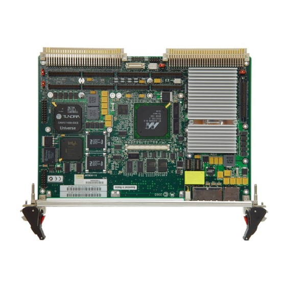
Motorola MVME5500 Manuals
Manuals and User Guides for Motorola MVME5500. We have
2
Motorola MVME5500 manuals available for free PDF download: Installation And Use Manual, Programmer's Reference Manual
Motorola MVME5500 Installation And Use Manual (148 pages)
Brand:
Motorola
| Category:
Motherboard
| Size: 0.77 MB
Table of Contents
Table of Contents
7
List of Figures
13
Summary of Changes
17
Overview of Contents
18
Comments and Suggestions
19
Conventions Used in this Manual
19
Description
21
Introduction
21
Getting Started
22
Overview of Startup Procedures
22
Table 1-1. Startup Overview
22
Unpacking Guidelines
22
Hardware Configuration
23
MVME5500 Preparation
24
Table 1-2. MVME5500 Jumper Settings
25
Figure 1-1. MVME5500 Layout
27
Ethernet
28
Ethernet 2, PMC/SBC Mode, and P2 I/O Selection Headers (J6, J7, J28, J32, J34, J97 - J110)
28
PMC/SBC Mode Selection
28
P2 I/O Selection
29
Flash 0 Programming Enable Header (J9)
31
Flash Boot Bank Select Header (J8)
31
Flash 0 Block Write Protect Header (J15)
32
Safe Start ENV Header (J10)
32
Powerpc Bus Mode Select Header (J19)
33
SROM Initialization Enable Header (J17)
33
CPU COP Enable Header (J20)
34
PCI Bus 0.0 Speed Header (J25)
34
PCI Bus 1.0 Speed Header (J29)
35
VME SCON Select Header (J27)
35
EEPROM Write Protect Header (J30)
36
Setting the PMC Vio Keying Pin
36
Hardware Installation
37
Installing the MVME5500 into a Chassis
37
Connection to Peripherals
38
Table 1-3. MVME5500 Connectors
38
Completing the Installation
39
Applying Power
41
Introduction
41
Switches and Indicators
41
Table 2-1. Front-Panel LED Status Indicators
42
Introduction
43
Motload Implementation and Memory Requirements
43
Overview
43
Motload Commands
44
Motload Tests
44
Motload Utility Applications
44
Command Line Interface
46
Using Motload
46
Command Line Help
47
Command Line Rules
48
Motload Command List
49
Table 3-1. Motload Commands
49
VME Settings
54
CR/CSR Settings
58
Displaying VME Settings
58
Editing VME Settings
59
Deleting VME Settings
60
Restoring Default VME Settings
60
Remote Start
61
Features
63
Table 4-1. MVME5500 Features Summary
63
Block Diagram
64
Figure 4-1. MVME5500 Block Diagram
65
L3 Cache
65
Processor
65
CPU Bus Interface
66
System Controller
66
I2C Serial Interface and Devices
67
Interrupt Controller
67
Memory Controller Interface
67
Direct Memory Access (DMA)
68
Timers
68
Flash Memory
69
System Memory
69
10/100Mb Ethernet Interface
70
Gigabit Ethernet Interface
70
PCI Local Buses and Devices
70
PCI Bus Arbitration
71
PCI IDSEL Definition
71
PCI-To-PCI Bridges
71
PMC Sites
71
Asynchronous Serial Ports
72
Figure 4-2. COM1 Asynchronous Serial Port Connections (RJ-45)
72
Real Time Clock and NVRAM
72
Sources of Reset
73
System Control and Status Registers
73
VME Interface
73
Debug Support
74
PMC Expansion
74
Introduction
75
Asynchronous Serial Port Connector (J1)
76
Connectors
76
Table 5-1. COM1 Connector (J1) Pin Assignments
76
Ethernet Connectors (J2)
77
IPMC Connector (J3)
77
Table 5-2. Ethernet Connector (J2) Pin Assignments
77
Table 5-3. IPMC Connector (J3) Pin Assignments
77
PCI/PMC Expansion Connector (J4)
79
Table 5-4. PCI/PMC Expansion Connector (J4) Pin Assignments
79
CPU COP Connector (J5)
82
PMC 1 Interface Connectors (J11, J12, J13, J14)
82
Table 5-5. CPU COP Connector (J5) Pin Assignments
82
Table 5-6. PMC 1 Connector (J11) Pin Assignments
83
Table 5-7. PMC 1 Connector (J12) Pin Assignments
84
Table 5-8. PMC 1 Connector (J13) Pin Assignments
86
Table 5-9. PMC 1 Connector (J14) Pin Assignments
87
Boundary Scan Connector (J18)
89
Table 5-10. Boundary Scan Connector (J18) Pin Assignments
89
PMC 2 Interface Connectors (J21, J22, J23, J24)
90
Table 5-11. PMC 2 Connector (J21) Pin Assignments
90
Table 5-12. PMC 2 Connector (J22) Pin Assignments
91
Table 5-13. PMC 2 Connector (J23) Pin Assignments
93
Table 5-14. PMC 2 Connector (J24) Pin Assignments
94
Asynchronous Serial Port (COM2) Planar Connector (J33)
96
Table 5-15. COM2 Planar Connector (J33) Pin Assignments
96
Vmebus Connectors (P1 & P2) (PMC Mode)
96
Table 5-16. VME Connector (P2) Pin Assignments (PMC Mode)
97
Vmebus Connectors (P1 & P2) (SBC Mode)
99
Table 5-17. VME Connector (P2) Pinout with IPMC712
100
Table 5-18. VME Connector (P2) Pinouts with IPMC761
101
Memory Expansion Connector (P4)
103
Table 5-19. Memory Expansion Connector (P4) Pin Assignments
103
Ethernet
107
Ethernet 2, PMC/SBC Mode, and P2 I/O Selection Headers (J6, J7, J28, J32, J34, J97 - J110)
107
Headers
107
PMC/SBC Mode Selection
108
Table 5-21. Ethernet 2 Selection Headers (J34, J97, J98, J99) Pin Assignments
108
P2 I/O Selection
109
Table 5-22. PMC/SBC Mode Selection Headers (J28, J32) Pin Assignments
109
Table 5-23. P2 I/O Selection Headers (J102 - J110) Pin Assignments
110
Figure 5-1. SBC/IPMC712 Mode
111
Figure 5-2. SBC/IPMC761 Mode
112
Figure 5-3. PMC Mode
113
Flash 0 Programming Enable Header (J9)
114
Flash Boot Bank Select Header (J8)
114
Table 5-24. Flash Boot Bank Select Header (J8) Pin Assignments
114
Table 5-25. Flash 0 Programming Enable Header (J9) Pin Assignments
114
Flash 0 Block Write Protect Header (J15)
115
Safe Start ENV Header (J10)
115
Table 5-26. Safe Start ENV Header (J10) Pin Assignments
115
Table 5-27. Flash 0 Write Protect Header (J15) Pin Assignments
115
Bus Mode Select Header (J19)
116
SROM Initialization Enable Header (J17)
116
Table 5-28. SROM Initialization Enable Header (J17) Pin Assignments
116
Table 5-29. Bus Mode Header (J19) Pin Assignments
116
COP Enable Header (J20)
117
PCI Bus 0.0 Speed Header (J25)
117
Table 5-30. COP Enable Header (J20) Pin Assignments
117
Table 5-31. PCI Bus 0.0 Speed Header (J25) Pin Assignments
117
PCI Bus 1.0 Speed Header (J29)
118
Table 5-32. VME SCON Select Header (J27) Pin Assignments
118
Table 5-33. PCI Bus 1.0 Speed Header (J25) Pin Assignments
118
VME SCON Select Header (J27)
118
EEPROM Write Protect Header (J30)
119
Table 5-34. EEPROM Write Protect Header (J30) Pin Assignments
119
Power Requirements
121
Supply Current Requirements
121
Table A-1. Power Requirements
121
Environmental Specifications
122
Table A-2. MVME5500 Specifications
122
APPENDIX B RAM5500 Memory Expansion Module
123
Features
123
Functional Description
123
Overview
123
RAM5500 Description
123
Srom
123
Table B-1. RAM5500 Feature Summary
123
Figure B-1. RAM5500 Block Diagram
124
Clocks
125
RAM5500 Module Installation
125
Memory Expansion Connector (P1) Pin Assignments
127
Table B-2. RAM5500 Connector (P1) Pin Assignments
127
RAM5500 Programming Issues
130
Serial Presence Detect (SPD) Data
130
Thermally Significant Components
131
Table C-1. Thermally Significant Components
132
Figure C-1. Thermally Significant Components-Primary Side
133
Figure C-2. Thermally Significant Components-Secondary Side
134
CHAPTER 1 Preparation
135
Measuring Junction Temperature
135
Measuring Case Temperature
135
Figure C-3. Mounting a Thermocouple under a Heatsink
137
Measuring Local Air Temperature
138
Figure C-4. Measuring Local Air Temperature
138
Table D-1. Motorola ECC Documents
139
Table D-2. Manufacturers' Documents
140
Table D-3. Related Specifications
143
Component Temperature Measurement
135
Advertisement
Motorola MVME5500 Programmer's Reference Manual (61 pages)
Brand:
Motorola
| Category:
Motherboard
| Size: 0.29 MB
Table of Contents
Table of Contents
7
List of Figures
9
About this Guide
11
Overview of Contents
11
Comments and Suggestions
12
Conventions Used in this Manual
12
CHAPTER 1 Board Description and Memory Maps
14
Introduction
14
Overview
14
Table 1-1. MVME5500 Features Summary
15
Memory Maps
18
Default Processor Memory Map
18
Table 1-2. Default Processor Memory Map
18
Motload's Processor Memory Map
19
Table 1-3. Motload's Processor Memory Map
19
Default PCI Memory Map
20
Table 1-4. Default PCI Memory Map
20
Motload's PCI Memory Maps
22
PCI I/O Space Maps
22
Table 1-5. Motload's PCI 0 Domain Memory Map
22
Table 1-6. Motload's PCI 1 Domain Memory Map
22
Table 1-7. PCI 0 Domain I/O Map
22
System I/O Memory Map
23
Table 1-8. PCI 1 Domain I/O Map
23
Table 1-9. Device Bank 1 I/O Memory Map
23
System Status Register 1
24
System Status Register 2
26
Table 1-11. System Status Register 2
26
System Status Register 3
28
Table 1-12. System Status Register 3
28
Presence Detect Register
29
Table 1-13. Presence Detect Register
29
Configuration Header/Switch Register (S1)
30
Table 1-14. Configuration Header/Switch Register
30
Time Base Enable Register
31
Geographical Address Register (S2)
31
Table 1-15. TBEN Register
31
Table 1-16. Geographical Address Register
32
COM1 & COM2 Universal Asynchronous Receiver/Transmitter (UART)
33
Real-Time Clock and NVRAM
33
ISA Local Resource Bus
33
CHAPTER 2 Programming Details
34
Introduction
34
PCI Configuration Space and IDSEL Mapping
34
Table 2-1. IDSEL Mapping for PCI Devices
35
Interrupt Controller
36
Table 2-2. GT-64260B External GPP Interrupt Assignments
37
Two-Wire Serial Interface
38
Table 2-3. I2C Bus Device Addressing
39
GT-64260B Initialization
40
GT-64260B GPP Configuration
40
Table 2-4. GT-64260B GPP Pin Function Assignments
41
GT-64260B Reset Configuration
42
Table 2-5. GT-64260B Power-Up Configuration Settings
43
GT-64260B Device Controller Bank Assignments
44
Table 2-6. Device Bank Assignments
45
Table 2-7. Device Bank Timing Parameters
45
System Clock Generators
46
VPD and User Configuration Eeproms
47
Temperature Sensor
47
Flash Memory
47
PCI Arbitration Assignments
47
Other Software Considerations
48
CPU Bus Mode
48
Table 2-8. PCI Arbiter Assignments
48
Processor Type Identification
49
Processor PLL Configuration
49
L1, L2, L3 Cache
49
Table 2-9. Processor L3CR Register Assignments
49
APPENDIX A Vital Product Data
51
Flash Memory Configuration Data
51
Table A-1. Flash 0 Memory Configuration Data
51
Table A-2. Flash 1 Memory Configuration Data
52
L3 Cache Configuration Data
53
Table A-3. L3 Cache Configuration Data
53
APPENDIX B Related Documentation
55
Motorola Computer Group Documents
55
Table B-1. Motorola Computer Group Documents
55
Manufacturers' Documents
56
Table B-2. Manufacturers' Documents
56
Related Specifications
59
Table B-3. Related Specifications
59
Advertisement
Related Products
Motorola MVME55006E
Motorola MVME2604-1031A
Motorola MVME2604-2191A
Motorola MVME166
Motorola MVME2700-14X1
Motorola MVME2700-1341
Motorola MVME2700-1361
Motorola MVME2700-4231A
Motorola MVME2700-3331
Motorola MVME2700-3361
Motorola Categories
Cell Phone
Two-Way Radio
Baby Monitor
Cordless Telephone
Radio
More Motorola Manuals
Login
Sign In
OR
Sign in with Facebook
Sign in with Google
Upload manual
Upload from disk
Upload from URL