
Related Manuals for Motorola MVME5500


Summary of Contents for Motorola MVME5500
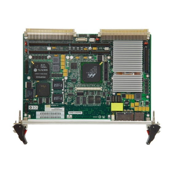
- Page 1 MVME5500 Single-Board Computer Programmer’s Reference Guide V5500A/PG1 August 2003 Edition...
- Page 2 All rights reserved. Printed in the United States of America. Motorola and the stylized M logo are trademarks of Motorola, Inc., registered in the U.S. Patent and Trademark Office. All other product or service names mentioned in this document are the property of their...
- Page 3 The safety precautions listed below represent warnings of certain dangers of which Motorola is aware. You, as the user of the product, should follow these warnings and all other safety precautions necessary for the safe operation of the equipment in your operating environment.
- Page 4 Flammability All Motorola PWBs (printed wiring boards) are manufactured with a flammability rating of 94V-0 by UL-recognized manufacturers. EMI Caution This equipment generates, uses and can radiate electromagnetic energy. It Caution may cause or be susceptible to electromagnetic interference (EMI) if not installed and used with adequate EMI protection.
- Page 5 Warning Motorola Computer Group products with the CE marking comply with the EMC Directive (89/336/EEC). Compliance with this directive implies conformity to the following European Norms: EN55022 “Limits and Methods of Measurement of Radio Interference Characteristics...
- Page 6 Electronic versions of this material may be read online, downloaded for personal use, or referenced in another document as a URL to the Motorola Computer Group Web site. The text itself may not be published commercially in print or electronic form, edited, translated, or otherwise altered without the permission of Motorola, Inc.
-
Page 7: Table Of Contents
Contents About This Guide Overview of Contents ....................xiii Comments and Suggestions ..................xiv Conventions Used in This Manual ................xiv CHAPTER 1 Board Description and Memory Maps Introduction ......................1-1 Overview ........................1-1 Memory Maps ......................1-5 Default Processor Memory Map ............... 1-5 MOTLoad’s Processor Memory Map ............... - Page 8 L1, L2, L3 Cache ..................... 2-16 APPENDIX A Vital Product Data Flash Memory Configuration Data ................A-1 L3 Cache Configuration Data .................. A-3 APPENDIX B Related Documentation Motorola Computer Group Documents ..............B-1 Manufacturers’ Documents ..................B-2 Related Specifications ..................... B-5 viii...
-
Page 9: List Of Figures
List of Figures Figure 1-1. MVME5500 Block Diagram ..............1-4... - Page 10 List of Tables Table 1-1. MVME5500 Features Summary ............1-2 Table 1-2. Default Processor Memory Map ............1-5 Table 1-3. MOTLoad’s Processor Memory Map ............ 1-6 Table 1-4. Default PCI Memory Map ..............1-7 Table 1-5. MOTLoad’s PCI 0 Domain Memory Map ..........1-9 Table 1-6.
-
Page 11: Overview Of Contents
MVME5500 family of boards. This document should be used by anyone who wants general, as well as technical information about the MVME5500 products. As of the printing date of this manual, the MVME5500 supports the models listed below. Model Number... -
Page 12: Comments And Suggestions
Comments and Suggestions Motorola welcomes and appreciates your comments on its documentation. We want to know what you think about our manuals and how we can make them better. Mail comments to: Motorola Computer Group Reader Comments DW164 2900 S. Diablo Way... - Page 13 <Enter>, <Return> or <CR> represents the carriage return or Enter key. Ctrl represents the Control key. Execute control characters by pressing the Ctrl key and the letter simultaneously, for example, Ctrl-d.
-
Page 14: Introduction
Introduction This chapter briefly describes the board level hardware features of the MVME5500 single-board computer, including a table of features and a block diagram. The remainder of the chapter provides memory map information including a default memory map, MOTLoad’s processor memory map, a default PCI memory map, MOTLoad’s PCI memory map,... -
Page 15: Table 1-1. Mvme5500 Features Summary
Board Description and Memory Maps The following table lists the features of the MVME5500. Table 1-1. MVME5500 Features Summary Feature Description Processor – Single 1 GHz MPC7455 processor – Bus clock frequency at 133 MHz L3 Cache – 2MB using DDR SRAM –... - Page 16 Overview Table 1-1. MVME5500 Features Summary (continued) Feature Description – Provided by GT-64260B – Master or slave capable – On-board serial EEPROMs for VPD, SPD, GT-64260B init, and user data storage NVRAM – 32KB provided by MK48T37 Real Time Clock –...
- Page 17 Board Description and Memory Maps Figure 1-1. MVME5500 Block Diagram Computer Group Literature Center Web Site...
-
Page 18: Memory Maps
2400 0000 25FF FFFF 32MB PCI Bus 1 Memory Space 1 2600 0000 27FF FFFF 32MB PCI Bus 1 Memory Space 2 2800 0000 29FF FFFF 32MB PCI Bus 1 Memory Space 3 2A00 0000 F0FF FFFF 3184MB Unassigned http://www.motorola.com/computer/literature... -
Page 19: Motload's Processor Memory Map
Board Description and Memory Maps Table 1-2. Default Processor Memory Map (continued) Processor Address Start Size Definition Notes F100 0000 F100 FFFF 64KB Internal Registers F101 0000 F1FF FFFF 16MB - Unassigned 64KB F200 0000 F3FF FFFF 32MB PCI Bus 0 Memory Space 1 F400 0000 F5FF FFFF 32MB... -
Page 20: Default Pci Memory Map
PCI Address Start Size Definition 0000 0000 007F FFFF SDRAM Bank 0 0080 0000 00FF FFFF SDRAM Bank 1 0100 0000 017F FFFF SDRAM Bank 2 0180 0000 01FF FFFF SDRAM Bank 3 0200 0000 0FFF FFFF 224MB Unassigned http://www.motorola.com/computer/literature... - Page 21 Board Description and Memory Maps Table 1-4. Default PCI Memory Map (continued) PCI Address Start Size Definition 1000 0000 11FF FFFF 32MB PCI Bus 1 P2P I/O Space 1200 0000 13FF FFFF 32MB PCI Bus 1 P2P Memory Space 0 1400 0000 1400 FFFF 64KB...
-
Page 22: Motload's Pci Memory Maps
PCI I/O Space Maps The PCI I/O space map for each PCI domain is shown in the following tables. Table 1-7. PCI 0 Domain I/O Map PCI 0 I/O Address Start Size Definition 0000 0000 007F FFFF Local PCI Domain I/O Space http://www.motorola.com/computer/literature... -
Page 23: System I/O Memory Map
Local PCI Domain I/O Space System I/O Memory Map System resources for the MVME5500 board including system control and status registers, NVRAM/RTC, and the 16550 UARTs are mapped into a 1MB address range assigned to device bank 1. The region defined by device bank 1 resides within the GT-64260B device bus register’s space... -
Page 24: System Status Register 1
System Status Register 1 System Status Register 1 The MVME5500 board system status register 1 is used to provide board status information and software control of Abort. Table 1-10. System Status Register 1 System Status Register 1 - Offset 0x0 0000... - Page 25 Board Description and Memory Maps ABORT_ This bit reflects the current state of the on-board abort signal. Writing a 0 at this bit position asserts the abort interrupt output signal, while writing a 1 at this bit position clears the abort interrupt output signal. Reading a 1 at this bit position indicates that the abort switch is deasserted, while reading a 0 at this bit position indicates that the abort switch is asserted.
-
Page 26: System Status Register 2
System Status Register 2 System Status Register 2 The MVME5500 board system status register 2 provides board control and status bits. Table 1-11. System Status Register 2 System Status Register 2 - Offset 0x0 0001 FIELD OPER RESET BD_FAIL Board fail. This bit is used to control the board fail LED. A set condition illuminates the front-panel LED and a cleared condition extinguishes the front-panel LED. - Page 27 M66EN pin. A cleared condition indicates that PCI Bus 0.0 is operating at 33 MHz. A set condition indicates that the bus is operating at 66 MHz. This bit is always cleared on the MVME5500. PCI1.0_M66EN PCI Bus 1.0 M66EN. This bit reflects the state of the PCI Bus 1.0 M66EN pin.
-
Page 28: System Status Register 3
OPER RESET BRD_RST Board reset. Setting this bit forces a hard reset of the MVME5500 board. This bit clears automatically when the board reset is complete. ABT_INT_MASK Abort interrupt mask. This bit is used to mask the abort interrupt. If this bit is set, the abort interrupt is masked so the abort interrupt is not generated. -
Page 29: Presence Detect Register
Board Description and Memory Maps Presence Detect Register The MVME5500 board contains a presence detect register that may be read by the system software to determine the presence of optional devices. Table 1-13. Presence Detect Register Presence Detect Register - Offset 0x0 0004h... -
Page 30: Configuration Header/Switch Register (S1)
Configuration Header/Switch Register (S1) Configuration Header/Switch Register (S1) The MVME5500 board has an 8-bit header or switch that may be read by the software. Table 1-14. Configuration Header/Switch Register Configuration Header/Switch Register - Offset 0x0 0005h FIELD OPER RESET CFG[7-0] Configuration bits 7-0. -
Page 31: Time Base Enable Register
Board Description and Memory Maps Time Base Enable Register The time base enable (TBEN) register provides the means to control the processor’s TBEN input. Table 1-15. TBEN Register TBEN Register- Offset 0x0 0006 FIELD OPER RESET TBEN0 Processor time base enable. When this bit is cleared, the TBEN pin of the processor is driven low. -
Page 32: Table 1-16. Geographical Address Register
Geographical Address Register (S2) Note The switch positions must all be turned off when the MVME5500 is used in a 5-row backplane. Table 1-16. Geographical Address Register Geographical Address Register - 0xFF100007 FIELD OPER RESET GAP* = 0 GAP* = 1... -
Page 33: Com1 & Com2 Universal Asynchronous Receiver/Transmitter (Uart)
1.8432 MHz. For additional programming details, refer to the PC16550 Data Sheet. Real-Time Clock and NVRAM The SGS-Thomson M48T37 is used by the MVME5500 board to provide 32KB of non-volatile static RAM, real-time clock, and watchdog timer functions. The device is accessed as linear memory. Refer to the MK48T37 Data Sheet for programming information. -
Page 34: Introduction
IDSEL assignments for the PCI devices on each of the PCI buses on the MVME5500 board along with the corresponding interrupt assignment to the general-purpose port (GPP) pins. Refer to the GT-64260B System Controller for PowerPC Processors Data Sheet and the PCI 6154 (HB2) -
Page 35: Table 2-1. Idsel Mapping For Pci Devices
Programming Details Documentation, for details on generating configuration cycles on each of the PCI buses. Table 2-1. IDSEL Mapping for PCI Devices Device INT# to GPP Interrupt Input Device Physical PCI Number Field Line Device INTA# INTB# INTC# INTD# 0b0_0001 AD11 IPMC 0b0_0110... -
Page 36: Interrupt Controller
GT-64260B PCI Bridge Interrupt Controller The MVME5500 uses the GT-64260B interrupt controller to handle interrupts internal to the GT-64260B, as well as the external interrupt sources. The GT-64260B has a limited number of directly triggerable interrupt inputs. Each of the GPP pins can be configured for an interrupt input, but the inputs are combined internally in groups of eight inputs (one for each byte lane) for one interrupt source. -
Page 37: Table 2-2. Gt-64260B External Gpp Interrupt Assignments
Programming Details the GT-64260B System Controller for PowerPC Processors Data Sheet, listed in Appendix B, Related Documentation, for details. Table 2-2. GT-64260B External GPP Interrupt Assignments Edge/ Group GPP # Level Polarity Interrupt Source Level High COM1 || COM2 Level Not Used. -
Page 38: Two-Wire Serial Interface
Unused. Pulled High. Unused. Pulled High. Two-Wire Serial Interface A two-wire serial interface for the MVME5500 board is provided by an I2C compatible serial controller integrated into the GT-64260B system controller. The I2C serial controller provides two basic functions. The first function is to provide GT-64260B register initialization following a reset. -
Page 39: Table 2-3. I2C Bus Device Addressing
Programming Details contained on the MVME5500 board, along with the SPD EEPROMs, to further initialize the memory controller and other interfaces. For additional details regarding the GT-64260B two-wire serial controller operation, refer to the GT-64260B System Controller for PowerPC Processors Data Sheet,... -
Page 40: Gt-64260B Initialization
GPP pins default to general-purpose inputs. Software must then configure each of the pins for the desired function. The following table defines the function assigned to each GPP pin on the MVME5500 board. Table 2-4. GT-64260B GPP Pin Function Assignments... -
Page 41: Table 2-4. Gt-64260B Gpp Pin Function Assignments
Programming Details Table 2-4. GT-64260B GPP Pin Function Assignments (continued) GPP Number Input/Output Function PMC 1 Interrupt INT B PMC 1 Interrupt INT C PMC 1 Interrupt INT D/IPMC INT VME Interrupt 0 VME Interrupt 1 VME Interrupt 2 VME Interrupt 3 PMC 2 Interrupt INT A PMC 2 Interrupt INT B PMC 2 Interrupt INT C... -
Page 42: Gt-64260B Reset Configuration
Partial pin sample on deassertion of reset plus serial ROM initialization via the I2C bus The MVME5500 board supports both options listed above. An on-board jumper setting is used to select the option. If the pin-sample-only method is selected, then states of the various pins on the device AD bus are sampled when reset is deasserted to determine the desired operating modes. -
Page 43: Table 2-5. Gt-64260B Power-Up Configuration Settings
Programming Details AD(30:28) – PLL settings AD(31) – CPU interface voltage Table 2-5. GT-64260B Power-Up Configuration Settings Default Device AD Select Power-Up Bus Signal Option Setting Description State of Bit vs. Function AD[0] Jumper SROM Initialization No SROM Initialization SROM Initialization Enabled AD[1] Resistor... -
Page 44: Gt-64260B Device Controller Bank Assignments
2.5V GT-64260B Device Controller Bank Assignments The MVME5500 board uses three of the GT-64260B device controller banks for interfacing to various devices. The following tables define the device bank assignments and the programmable device bank timing parameters required for each of the banks used. Note that all device bank http://www.motorola.com/computer/literature... -
Page 45: Table 2-6. Device Bank Assignments
Programming Details timing parameters, except BAdrSkew, have an extension bit that forms the most significant bit of the timing parameter. Table 2-6. Device Bank Assignments Device Bank Data Width Function Note 32 bit Flash 0 Soldered Flash or Flash 1 Soldered Flash 8 bit I/O Devices Not used... -
Page 46: System Clock Generators
PLL clock generators. The clock tree is designed in such a manner as to maintain the strict edge-to-edge jitter and low clock- to-clock skew required by these devices. Additional clocks required by individual devices are generated near the devices using individual oscillators. http://www.motorola.com/computer/literature 2-13... -
Page 47: Vpd And User Configuration Eeproms
Flash Memory The MVME5500 contains two banks of Flash memory accessed via the device controller contained within the GT-64260B. Flash 1 consists of two soldered 32Mb devices (E28F320J3A) to give a minimum of 8MB Flash memory. -
Page 48: Other Software Considerations
Other Software Considerations The following subsections discuss software aspects of the CPU bus, processor, and cache that can have an influence on the MVME5500. CPU Bus Mode The CPU bus operating mode (60x or MPX) is determined by reading the BMODE bits (bits 16-17) in the processor’s Memory Subsystem Control... -
Page 49: Processor Type Identification
The processors support on-chip L1 and L2 caches and external L3 cache. L3 cache supports 1 or 2MB in a variety of SRAM device types. Each processor L3 interface on the MVME5500 consists of two 8Mb devices (K7D803671B-HC30) providing a total of 2MB of L3 cache. Data parity checking should be enabled. - Page 50 Table 2-9. Processor L3CR Register Assignments Apollo L3CR Register Description Value L3PE L3 Data Parity Checking Enable, ON L3CLK L3 Clock Speed; 233 MHz, Divide by 4 110 L3CKSP L3 Clock Sample Point, 2 Clocks L3PSP L3 P-Clock Sample Point, 3 Clocks http://www.motorola.com/computer/literature 2-17...
-
Page 51: Flash Memory Configuration Data
(Bytes) Field Mnemonic Field Description FMC_MID Manufacturer’s Identifier FMC_DID Manufacturer’s Device Identifier FMC_DDW Device Data Width (16 bits on MVME5500) FMC_NOD Number of Devices Present (two on MVME5500) FMC_NOC Number of Columns (Interleaves) (two on MVME5500) FMC_CW Column Width in Bits (16 on MVME5500) This will always be a multiple of the device’s... -
Page 52: Table A-2. Flash 1 Memory Configuration Data
Field Description FMC_MID Manufacturer’s Identifier (FFFF = Undefined/Not-Applicable) FMC_DID Manufacturer’s Device Identifier (FFFF = Undefined/Not-Applicable) FMC_DDW Device Data Width (16 bits on MVME5500) FMC_NOD Number of Devices Present (two on MVME5500) FMC_NOC Number of Columns (Interleaves) (two on MVME5500) FMC_CW Column Width in Bits (16 on MVME5500) This will always be a multiple of the device’s... -
Page 53: L3 Cache Configuration Data
Offset (Bytes) Field Mnemonic Field Description FMC_WEDW Write/Erase Data Width (16 on MVME5500) The two memory devices must be programmed in parallel when the write/erase data width exceeds the device’s data width. FMC_BANK Bank Number of Memory Array: 1 for this... - Page 54 Vital Product Data Table A-3. L3 Cache Configuration Data (continued) Byte Offset Field Size (Bytes) Field Description Processor clock sample point: 03 - 3 clocks Sample point override: 00 - sample point override disabled SRAM clock control: 00 - SRAM clock control disabled SRAM type: 00 - MSUG2 DDR SRAM Data bus error detection type:...
-
Page 55: Motorola Computer Group Documents
BRelated Documentation Motorola Computer Group Documents The Motorola publications listed below are referenced in this manual. You can obtain electronic copies of Motorola Computer Group publications by: Contacting your local Motorola sales office Visiting Motorola Computer Group’s World Wide Web literature site, http://www.motorola.com/computer/literature... -
Page 56: Manufacturers' Documents
Table B-2. Manufacturers’ Documents Document Title and Source Publication Number MPC7450 RISC Microprocessor User’s Manual MPC7450UM/D Rev 2 Literature Distribution Center for Motorola Telephone: 1-800- 441-2447 FAX: (602) 994-6430 or (303) 675-2150 Web Site: http://e- www.motorola.com/webapp/sps/library/prod_lib.jsp E-mail: ldcformotorola@hibbertco.com... - Page 57 3 Volt Intel StrataFlash Memory 290667-005 28F128J3A, 28F640J3A, 28F320J3A Intel Corporation Literature Center 19521 E. 32nd Parkway Aurora CO 80011-8141 Web Site: http://www.intel.com/design/litcentr/index.htm PCI 6154 (HB2) PCI-to-PCI Bridge Data Book 6154_DataBook_v2.0.p PLX Technology, Inc. 870 Maude Avenue Sunnyvale, California 94085 Web Site: http://www.hintcorp.com/products/hint/default.asp http://www.motorola.com/computer/literature...
- Page 58 Related Documentation Table B-2. Manufacturers’ Documents (continued) Document Title and Source Publication Number TL16C550C Universal Asynchronous Receiver/Transmitter SLLS177E Texas Instruments P. O. Box 655303 Dallas, Texas 75265 Web Site: http://www.ti.com 3.3V-5V 256Kbit (32Kx8) Timekeeper SRAM M48T37V ST Microelectronics 1000 East Bell Road Phoenix, AZ 85022 Web Site: http://eu.st.com/stonline/index.shtml...
-
Page 59: Related Specifications
Publication Number VITA http://www.vita.com/ VME64 Specification ANSI/VITA 1-1994 VME64 Extensions ANSI/VITA 1.1-1997 2eSST Source Synchronous Transfer VITA 1.5-199x PCI Special Interest Group (PCI SIG) http://www.pcisig.com/ Peripheral Component Interconnect (PCI) Local Bus Specification, PCI Local Bus Revision 2.0, 2.1, 2.2 Specification http://www.motorola.com/computer/literature... - Page 60 Index interrupt controller block diagram L1, L2, L3 cache 2-16 L3 cache config data cache 2-16 comments, sending config switch register 1-17 manual conventions conventions used in the manual manufacturers’ documents core frequency 2-16 memory maps CPU bus mode 2-15 default PCI default processor MOTLoad’s PCI...
- Page 61 time base enable register 1-18 time base enable register 1-18 related documentation two-wire serial interface typeface, meaning of suggestions, submitting system clock generators 2-13 system I/O memory map 1-10 UART 1-20 system status register 1 1-11 system status register 2 1-13 system status register 3 1-15...