Table of Contents
Advertisement
Notes: Please refer to the original service manual for:
• Speaker system SB-BTT775EBK, Order No: PSG1103006CE
TABLE OF CONTENTS
1 Safety Precautions----------------------------------------------- 3
1.1. GENERAL GUIDELINES -------------------------------- 3
1.2. Before Use -------------------------------------------------- 3
1.3. Before Repair and Adjustment ------------------------- 3
1.4. Protection Circuitry ---------------------------------------- 4
1.5. Safety Parts Information --------------------------------- 5
2 Warning -------------------------------------------------------------- 6
TM
Blu-ray Disc
Model No.
Vol.1
Product Color: (K)...Black Type
PAGE
3 Service Navigation --------------------------------------------- 10
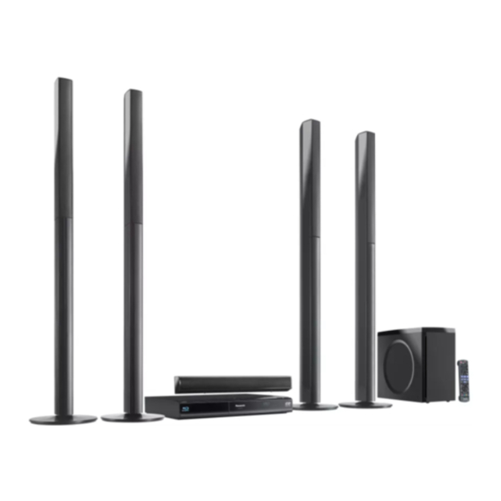
Home Theater Sound System
SA-BTT775GA
SA-BTT775PU
to Electrostatic Sensitive (ES) Devices---------------6
2.2. Precaution of Laser Diode -------------------------------7
2.4. Handling Precaution for Traverse Unit----------------8
3.1. Service Information -------------------------------------- 10
© Panasonic Corporation 2011. All rights reserved.
Unauthorized copying and distribution is a violation
of law.
PSG1104020CE
PAGE
Advertisement
Table of Contents

Related Manuals for Panasonic SA-BTT775GA


Summary of Contents for Panasonic SA-BTT775GA
-
Page 1: Table Of Contents
2.4. Handling Precaution for Traverse Unit----------------8 1.5. Safety Parts Information --------------------------------- 5 3 Service Navigation --------------------------------------------- 10 2 Warning -------------------------------------------------------------- 6 3.1. Service Information -------------------------------------- 10 © Panasonic Corporation 2011. All rights reserved. Unauthorized copying and distribution is a violation of law. - Page 2 3.2. Combination of Multiple Pressing on the 10.24. Replacement of Thermal Diode (D5802) --------- 107 Remote Control ------------------------------------------- 10 10.25. Replacement of Regulator Diode (D5803) ------- 108 3.3. Entering Special Modes with Combination of 11 Service Position------------------------------------------------ 110 Multiple Pressing on the Remote Control ---------- 10 11.1.
-
Page 3: Safety Precautions
1 Safety Precautions 1.1. GENERAL GUIDELINES 1. When servicing, observe the original lead dress. If a short circuit is found, replace all parts which have been overheated or damaged by the short circuit. 2. After servicing, see to it that all the protective devices such as insulation barriers, insulation papers shields are properly installed. -
Page 4: Protection Circuitry
1.3.1. Caution for fuse replacement 1.4. Protection Circuitry The protection circuitry may have operated if either of the following conditions are noticed: • No sound is heard when the power is turned on. • Sound stops during a performance. The function of this circuitry is to prevent circuitry damage if, for example, the positive and negative speaker connection wires are “shorted”, or if speaker systems with an impedance less than the indicated rated impedance of the amplifier are used. -
Page 5: Safety Parts Information
1.5. Safety Parts Information Safety Parts List: There are special components used in this equipment which are important for safety. These parts are marked by ( ) in the Schematic Diagrams & Replacement Parts List. It is essential that these critical parts should be replaced with manufacturer’s specified parts to prevent shock, fire or other hazards. -
Page 6: Warning
2 Warning 2.1. Prevention of Electrostatic Discharge (ESD) to Electrostatic Sensitive (ES) Devices Some semiconductor (solid state) devices can be damaged easily by static electricity. Such components commonly are called Elec- trostatically Sensitive (ES) Devices. Examples of typical ES devices are integrated circuits and some field-effect transistors and semiconductor “chip”... -
Page 7: Precaution Of Laser Diode
2.2. Precaution of Laser Diode Caution: This product utilizes a laser diode with the unit turned “on”, invisible laser radiation is emitted from the pickup lens. Wavelength: 790 nm (CDs), 655 nm (DVDs), 405 nm (BDs) Maximum output radiation power from pickup: 100 µW/VDE Laser radiation from the pickup unit is safety level, but be sure the followings: 1. -
Page 8: Service Caution Based On Legal Restrictions
2.3. Service caution based on Legal restrictions The lead free solder has been used in the mounting process of all electrical components on the printed circuit boards used for this equipment in considering the globally environmental conservation. The normal solder is the alloy of tin (Sn) and lead (Pb). On the other hand, the lead free solder is the alloy mainly consists of tin (Sn), silver (Ag) and Copper (Cu), and the melting point of the lead free solder is higher approx.30 degrees C (86°F) more than that of the normal solder. - Page 9 ble cable, cut off the antistatic FPC. Figure 1 Grounding for electrostatic breakdown prevention 2.4.2. Some devices such as the DVD player use the optical pickup (laser diode) and the optical pickup will be damaged by static electric- ity in the working environment. Proceed servicing works under the working environment where grounding works is completed. 2.4.2.1.
-
Page 10: Service Navigation
3 Service Navigation 3.1. Service Information This service manual contains technical information which will allow service personnel’s to understand and service this model. Please place orders using the parts list and not the drawing reference numbers. If the circuit is changed or modified, this information will be followed by supplement service manual to be filed with the original ser- vice manual. - Page 11 3.3.1. Disclosure mode (Combination of multiple pressing: [OK] [BLUE] [YELLOW]) Press and hold [OK] [BLUE] [YELLOW] on the remote control simultaneously for 5sec., then “00 RET” is displayed on FL display window. Remarks 3.3.2. Nondisclosure mode 1 (Combination of multiple pressing: [6] [7] [Yellow]) Press and hold [6] [7] [Yellow] on the remote control simultaneously for 5sec., then “50 RET”...
- Page 12 3.3.3. Nondisclosure mode 2 (Combination of multiple pressing: [5] [9] [Red]) Press and hold [5] [9] [Red] on the remote control simultaneously for about 5sec., then “70 RET” is displayed on FL display window. Remarks...
-
Page 13: Caution For Replacing Parts
Perform playback for one minute using the RAM disc. No abnormality should be seen in the picture, sound or operation. *Panasonic DVD-RAM disc should be used when recording and play- back. Perform playback for one minute using the BD-Video disc. - Page 14 Item Contents Check Item Contents Check Picture Block noise Sound Distorted sound Crosscut noise Noise (static, background noise, etc.) Dot noise The sound level is too low. Picture disruption The sound level is too high. Not bright enough The sound level changes. Too bright Flickering color Color fading...
-
Page 15: Specifications
4 Specifications WLAN Antenna: Tx 1, Rx 2 Standard Complaince: IEEE802.11n / IEEE802.11a IEEE802.11g / IEEE802.11b Main unit SA-BTT775GA/PU Transmission System: MISO-OFDM system, OFDM GENERAL system, DSSS system Power supply: AC 110 V to 127 V, Transfer rate (Standard): AC 220 V to 240 V, 50/60 Hz IEEE802.11n:... -
Page 16: Others (Licenses)
4.1. Others (Licenses) -
Page 17: Location Of Controls And Components
5 Location of Controls and Components 5.1. Remote Control Key Button Operations... -
Page 18: Main Unit Key Button Operations
5.2. Main Unit Key Button Operations OPEN/CLOSE Pull open. iPod SD CARD Standby/on switch ( /I) Start play Press to switch the unit from on to standby mode or vice SD card slot versa. In standby mode, the unit is still consuming a small USB port amount of power. -
Page 19: Speaker Connection
5.3. Speaker Connection... -
Page 20: Connection To A Broadband Network
For up to date compatibility information on your Wireless router refer to ht tp://panasonic .jp /sup por t/glo bal/cs/ (This site is in English only.) The unit is not compatible with public wireless LAN services provided in airports, stations, cafes etc. -
Page 21: Network Easy Setting
5.5. Network Easy Setting Network Easy Setting When you select “Yes” (For Malaysia, Thailand, Singapore and Hong Kong) For Asia Select “Wired” or “Wireless” and press [OK]. Network Easy Setting After completing “Easy setup”, you can perform “Network Easy Settings and tests for connection required Setting”. -
Page 23: Firmware Updates
5.6. Firmware Updates... -
Page 24: Enjoying Bd-Live Or Picture In Picture In Bd-Video
5.7. Enjoying BD-LIVE or picture in picture in BD-Video... -
Page 25: Regarding Divx
5.8. Regarding Divx... -
Page 26: Enjoying 3D Video
5.9. Enjoying 3D Video... -
Page 27: Using The Ipod/Iphone
5.10. Using the iPod/iPhone 5.10.1. iPod /iPhone Connection... - Page 28 5.10.2. iPod /iPhone Playback...
-
Page 29: Enjoying Viera Cast
5.11. Enjoying VIERA CAST... -
Page 30: Playing Back Contents On The Dlna Server (Dlna)
5.12. Playing Back Contents on the DLNA Server (DLNA) -
Page 31: Playable Disc/Cards
5.13. Playable disc/Cards... -
Page 32: File Extension Type Support (Mp3/Jpeg/Divx/Mkv)
5.14. File Extension Type Support (MP3/JPEG/DivX/MKV) -
Page 33: Operating Instructions
6 Operating Instructions 6.1. Removing of disc during abnormality 6.1.1. Using main unit key buttons. 6.1.1.1. When the power can be turned off. 1. Turn off the power and press & hold [OK] button on main unit, and [B] & [Y] button on remote for 5 seconds. 6.1.1.2. - Page 34 3. Gently pull out the tray. 4. Remove disc.
-
Page 35: Self-Diagnostic And Special Mode Setting
7 Self-Diagnostic and Special Mode Setting 7.1. Special Mode Setting 7.1.1. Special Mode Table 1 SERV... - Page 36 7.1.2. Special Mode Table 2 Item FL display Key operation Mode name Description Front Key Demonstration Ejection of the disc is prohibited. *When lock the tray. When the power is on (SS mode), lock/unlock The lock setting is effective until unlocking the press [PLAY] and [OPEN/CLOSE] tray and not released by Main unit keys simultaneously for 5 seconds.
- Page 37 7.1.3. Special Mode Table 3 Item FL display Key operation Mode name Description Front Key Progressive initialization The progressive setting is initialized to Inter- display before execution When the power is on (SS mode), lace. leaves. press [STOP] and [PLAY] simulta- neously for 5 seconds.
-
Page 38: Self-Diagnostic Function - Error Code
7.2. Self-Diagnostic Function - Error Code Self-Diagnostic Function provides information for error to service personnel by Self-Diagnosis Display when any error has occurred. U**, H** and F** are stored in my memory and held. • You can check latest error code by transmitting [0] [1] of Remote Control in Service Mode. Automatic Display on FL will be cancelled when the power is turned off or AC input is turned off during self-diagnosis display is 7.2.1. - Page 39 7.2.2. Error Code Table 2 (For BD) Error Code Diagnosis contents Description Monitor Display Automatic FL display SELF Restoration operation Since the power cord fell out during a power No display SELF CHECK CHECK failure or operation, it is under restoration operation.
-
Page 40: Service Mode
7.3. Service Mode Information necessary for service can be displayed. Service mode setting: 1. Turn the power off. 2. Press the [5] [9] and [R] button simultaneously for five seconds, then [70 FRET] is displayed on FL. 3. Press the [ ] or [ ] button to select until [80 SRV] is displayed on FL. - Page 41 7.3.1. Service Mode Table 1 7.2. Self-Diagnos- tic Functions Error code. 6. BOOT2 version 7. BOOT3 version Checking whether the drive is applicable When the drive is applicable drive. drive or not When the drive is not applicable drive. Mechanism. When BD Mechanism is OK When BD Mechanism is NG...
- Page 42 7.3.2. Service Mode Table 2 Item FL display Key operation Mode name Description (Remote controller key) Laser Used Time Check laser used time (hours) of BD Press [4] [1] in service mode. Indication Mechanism. ****** (******) is the used time display in hour.
- Page 43 7.3.3. Service Mode Table 3 Item FL display Key operation Mode name Description (Remote controller key) BD Mechanim last error BD Mechanism error code display . 1. Error Number is displayed for 5 Press [4] [2] in service mode. seconds. **** 2.
- Page 44 7.3.4. Service Mode Table 4 Item FL display Key operation Mode name Description (Remote controller key) 6. Disc maker ID is displayed for 5 In case that the maker cannot be seconds. identified, display is blackout. 7. Factor of drive error (hexadeci- mal) occurring is left displayed.
- Page 45 7.3.5. Service Mode Table 5 Item FL display Key operation Mode name Description (Remote controller key) && 8. When the last error doesn’t exist NO DATA CEC (H) output Check of the CEC terminal high output of Press [5] [5] in service mode. HDMI.
- Page 46 7.3.6. Service Mode Table 6...
-
Page 47: Troubleshooting Guide
8 Troubleshooting Guide 8.1. Troubleshooting Guide for F61 and/or F76 Set cannot Power ON: 1) Refer to Fig. 1. SMPS P.C.B. Condition 1: With 2) Refer to Schematic Diagram of Photocoupler PC5702, PC5702/PC5799 solder crack, Stanby LED on SMPS Circuit (Item 17.7) PC5799 dry joint ,short circuit,open circuit,etc... - Page 48 8.1.1. SMPS P.C.B. Transformer: T5701 Photocouple: PC5720 Thermal Diode: D5802 Switching Regulator IC: IC5701 Switching IC: IC5799 Photocouple: PC5702, PC5799 Figure 1. SMPS P.C.B.
- Page 49 8.1.2. Digital P.C.B. (Side A of Digital P.C.B.) Transistor : Q2903 INTEGRATED CIRCUIT : IC2901 Resistor : R2908 Inductor : LB2843 Transistor : Q2902 (Side B of Digital P.C.B.) Resistor : R7003 Transistor : QR7071 Inductor : L2902 Inductor : L2908 Fig 2.
-
Page 50: Service Fixture & Tools
9 Service Fixture & Tools 9.1. Service Tools and Equipment Prepare service tools before process service position. Ref. No Service Tools Remarks SFT1 Digital P.C.B. (CN2002) - Panel P.C.B. (P6001) RFKZBTT270K1 (13P FFC) SFT2 Digital P.C.B. (CN2004) - SMPS P.C.B. (JW2) RFKZBTT270K2 (10P FFC) SFT3 Digital P.C.B. -
Page 51: Disassembly And Assembly Instructions
10 Disassembly and Assembly Instructions Caution Note: • This section describes the disassembly and/or assembly procedures for all major printed circuit boards & main compo- nents for the unit. (You may refer to the section of “Main components and P.C.B Locations” as described in the service manual) •... -
Page 53: Disassembly Flow Chart
10.1. Disassembly Flow Chart 10.3.Top Cabinet 10.8. Front Panel 10.4. Wireless Adapter 10.15. BD Mechanism Unit Block Assembly P.C.B. (BRS1P) 10.15.1 . Dust cover 10.9. Panel P.C.B. 10.5. Rear Panel 10.15.2. Tray 10.10. Operation Button 10.6. Voltage Selector P.C.B. P.C.B. 10 .15.3 . -
Page 54: Main Components And P.c.b. Locations
10.2. Main Components and P.C.B. Locations... -
Page 55: Disassembly Of Top Cabinet
10.3. Disassembly of Top Cabinet Step 1 Remove 3 screws. Step 2 Remove Top Cabinet Ornament. Caution: During assembling, ensure that the catches of Top Cabinet Ornament are fully slotted to the holes on Top Cabinet. Step 3 Remove 2 screws. Step 7 Remove the Top Cabinet. -
Page 56: Disassembly Of Wireless Adapter P.c.b
Caution: During assembling, ensure that the Gasket is 10.4. Disassembly Wireless properly inserted & fully fixed onto Bottom Chassis. Adapter P.C.B. • Refer to “Disassembly of Top Cabinet”. Step 1 Remove 1 screw. Step 2 Press the Transmitter Chassis Unit downward to release from the catch. -
Page 57: Disassembly Of Rear Panel
Step 4 Detach 17P FFC at the connector (CN3001) on Wire- Step 7 Remove Wireless Adapter P.C.B.. less Adapter P.C.B.. Caution: During assembly, ensure Wireless Ground Spring is properly inserted and fully catched onto Wireless Adapter P.C.B.. Step 5 Remove 1 screw. Step 6 Release 2 catches. -
Page 58: Disassembly Of Voltage Selector P.c.b
10.6. Disassembly of Voltage Selec- tor P.C.B. • Refer to “Disassembly of Top Cabinet” Step 1 Remove 1 screw. Step 2 Release the Blue Wire (TL30) and White Wire (TL31) from cord holder. Caution: During assembling, ensure that Blue Wire (TL30) &... -
Page 59: Disassembly Of Fan
Step 4 Remove 2 screws. Step 5 Remove Voltage Selector Bracket. Caution: During assembling, ensure that Voltage Selector P.C.B. is properly fixed onto Voltage Selector Bracket before screwing. Step 3 Remove 2 screws. Step 6 Desolder Blue Wire (TL30) and White Wire (TL31) on Step 4 Lift up to remove Fan. - Page 60 Caution: Do not exert strong force when releasing the tabs. During assembling, ensure that Front Panel Block Assem- bly is properly inserted & fully catched onto Bottom Chas- sis. Step 7 Release tabs at both sides of the Front Panel Block Assembly in the direction of arrow.
-
Page 61: Disassembly Of Panel P.c.b
Caution (1): During assembling, ensure that 5P Cable, 11P FFC & 3P Wire are properly dressed through slots of Bot- tom Chassis. Caution (2): During assembling, ensure that 3P Wire is properly dressed on top of Bottom Chassis. Caution: During assembling, ensure that Panel P.C.B. is inserted under the rib of Bottom Chassis and properly located onto Bottom Chassis. - Page 62 Caution: During assembling, ensure that 3P Wire is prop- erly dressed in between wall & ribs of Front Panel as dia- gram shown. Step 4 Desolder pins of the connector (H6001) on Operation Button P.C.B.. Step 5 Remove the Operation Button P.C.B.. Step 2 Lift up the Operation Button P.C.B.
-
Page 63: Disassembly Of Power Button P.c.b
10.11. Disassembly of Power Button Step 3 Release 3P Wire from wall & ribs of Front Panel. Caution: During assembling, ensure that 3P Wire is prop- P.C.B. erly dressed in between wall & ribs of Front Panel as dia- gram shown. •... -
Page 64: Disassembly Of Ipod Cradle Assembly
10.12. Disassembly of iPod Cradle Step 7 Lift up the tesa tape. Caution: Replace the tesa tape if torn. Assembly • Refer to “Disassembly of Top Cabinet”. • Refer to “Disassembly of Front Panel Block Assembly”. Step 1 Open the iPod Cradle Assembly as diagram shown. Step 2 Release 2 catches. -
Page 65: Disassembly Of Ipod P.c.b
Caution: During assembling, ensure that Cradle Tub is properly fixed & fully catched into iPod Guide before screwing. 10.13. Disassembly of iPod P.C.B. • Refer to “Disassembly of Top Cabinet”. • Refer to “Disassembly of Front Panel Block Assembly”. • Refer to “Disassembly of iPod Cradle Assembly”. Step 1 Remove 2 screws. -
Page 66: Replacement Of Front Lid Assembly
10.14.2. Assembly of Front Lid Assembly Step 1 Apply hanarl around the 5 shafts as shown in the dia- gram. 10.14. Replacement Front Assembly 10.14.1. Disassembly of Front Lid Assembly • Refer to “Disassembly of Top Cabinet”. • Refer to “Disassembly of Front Panel Block Assembly”. Step 1 Release the Front Lid Spring by using a Flat head screwdriver in the direction of arrow. - Page 67 Caution: Ensure that the Front Lid Assembly are fully Step 4 Push Front Lid Assembly to the end according to direc- inserted into Front Panel. tion of arrow. Step 5 Apply grease around the shafts of Front Panel & Front Lid as diagram shown.
-
Page 68: Disassembly Of Bd Mechanism Unit (Brs1P)
10.15. Disassembly of BD Mecha- nism Unit (BRS1P) • Refer to “Disassembly of Top Cabinet”. Step 1 Open the Front Lid Assembly. Step 2 Insert Paper Clip into the bottom of the unit. Step 3 Push the paper clip in the direction of arrow to eject tray. Step 4 Slide the Tray out fully as direction of arrow. - Page 69 Step 5 Upset the unit. Caution: During assembling, ensure that Tray Ornament’s guide rib is properly inserted onto Tray. Step 6 Release 2 catches. Caution: During assembling, ensure that Tray Ornament is properly inserted & fully catched onto Tray. Step 7 Remove Tray Ornament in the direction of arrow. Step 8 Slide the tray in fully as direction of arrow.
- Page 70 Step 9 Detach 4P FFC at the connector (P55006) on Digital P.C.B.. Step 10 Detach 45P FFC at the connector (P55001) on Digital P.C.B.. Step 11 Detach 5P FFC at the connector (P55007) on Digital P.C.B.. Step 12 Detach 5P FFC at the connector (P55008) on Digital P.C.B..
- Page 71 10.15.1. Disassembly of Dust Cover 10.15.2. Replacement of Tray Step 1 Release the Dust Cover from the guides. Refer to “Disassembly of Dust Cover”. 10.15.2.1. Disassembly of Tray Step 1 Use a pin to push the Slide Cam until it come to a stop. The Tray will open automatically.
- Page 72 Step 3 Push the catches side way & remove the tray. Step 2 Align the guides of the Slide Cam with the groove of the tray unit. 10.15.2.2. Assembly of Tray Step 1 Insert the Tray into the guide rails as picture shown.
- Page 73 Step 3 Gently push in the tray unit until it is closed fully. Caution: Do not use strong force during pushing of the tray unit. Repeat Step 1 to Step 2, when the tray unit cannot be push forwards. Step 2 Lift up the FFC Plastic Sheet. Step 3 Release 45P FFC from the slots.
- Page 74 Step 4 Release 5P FFC from the BD Mechanism Unit (BRS1P). Step 5 Release 4P FPC from the BD Mechanism Unit (BRS1P). Caution: Avoid using strong force, to prevent damage on the solder area of 4P FPC. Step 6 Press down the hook. Step 7 Lift up the Turning Shaft of the Mid Base Unit as shown.
- Page 75 Step 8 Press down the hook. Step 10 Align the bosses of the Mid Base Unit with the grooves Step 9 Release the Turning Shaft of the Mid Base Unit as of the Slide Cam. shown. Step 11 Slightly tilt and lift up the arm of Mid Base at location as shown.
- Page 76 Step 12 Hold the arms of Mid Base, slightly pull backward and Step 15 Insert the Screwdriver at the Damper (Location B). lift up the Traverse Deck as shown. Step 16 Push up the Traverse Deck as shown. Step 17 Remove the Traverse Deck. Caution: During dissemble, ensure the Traverse Deck do not hit to the Slide Cam.
- Page 77 Step 23 Remove Traverse Deck as shown. Step 21 Insert the Screwdriver to the Damper as shown condi- tion. Step 22 Push up the Mid Base while screwdriver are inserted as shown.
- Page 78 10.15.3.2. Assembly of Traverse Unit Step 1 Align the Mid Base parallel with Traverse unit. Step 2 Push to fix Mid Base into the Damper as shown. Caution: Ensure the Mid Base is seated properly. Step 5 Insert the Traverse Deck underneath of the chassis plate.
- Page 79 Step 6 Align the damper on Traverse Deck with the slot of the Caution: During assembling, ensure the BD Traverse inserted fully. chassis of BD Mechanism Unit (BRS1P) as shown. Caution: During assembling, ensure the Traverse Deck do not hit to the Slide Cam. Step 8 Push the Slide Cam sidewards.
- Page 80 Step 9 Align the grooves of the Slide Cam with the bosses of Caution: Ensure the bosses on the Mid Base is seated properly into the shaft of the Slide Cam. the Mid Base. Step 10 Hold the Slide Cam, slightly pull backward the Mid Step 11 Push and press the turning shaft of the Mid Base side- Base and insert it into the grooves of the Slide Cam.
- Page 81 Step 12 Push and press the turning shaft of the Mid Base side- Step 13 Slide the Slide Cam until it come to a stop. way, a “click” sound is heard when is fully insert. Step 14 Insert OPU FFC Sheet as show a “click” sound is heard when the OPU FFC is fully catched.
- Page 82 Step 15 Insert 45P FFC into the guides. Step 16 Insert 4P FPC into the guides. Step 17 Insert 5P FFC into the guides. 10.15.3.3. Checking point after replacement of Traverse Unit Step 1 When Traverse unit in up position. Ensure the gap between Clamper and Mecha Chassis should more that 0.4mm to prevent rubbing.
- Page 83 10.15.4. Replacement of Slide Cam Step 3 Pull forward catches as shown to release Slide Cam. Refer to “Disassembly of Dust Cover”. Refer to “Disassembly of Tray”. Refer to “Disassembly of Traverse Unit”. 10.15.4.1. Disassembly of Slide Cam Step 1 Insert the screwdriver into the U-shape hole and release the guide as shown Step 2 Slide the Slide Cam to the end.
- Page 84 10.15.4.2. Assembly of Slide Cam Step 3 Press the Slide Cam and make sure it is fully catched onto the BD Mechanism Unit (BRS1P). Step 1 Place the Slide Cam into the BD Mechanism Unit (BRS1P) as shown. Step 2 Slide the Slide Cam to the end as shown & flip over the BD Mechanism Unit (BRS1P).
- Page 85 10.15.5. Replacement of Belt 10.15.5.2. Assembly of Belt Refer to “Disassembly of Dust Cover”. Step 1 Install Belt. Refer to “Disassembly of Tray”. Refer to “Disassembly of Traverse Unit”. Refer to “Disassembly of Slide Cam”. 10.15.5.1. Disassembly of Belt Step 1 Remove the Belt as shown.
- Page 86 10.15.6. Replacement of Pulley Gear 10.15.6.2. Assembly of Pulley Gear Refer to “Disassembly of Dust Cover”. Step 1 Fix the Pulley Gear into the boss a “click” sound is Refer to “Disassembly of Tray”. heard. Refer to “Disassembly of Traverse Unit”. Refer to “Disassembly of Slide Cam”.
- Page 87 10.15.7. Replacement of Driver Gear 10.15.8. Replacement of Loading P.C.B. Refer to “Disassembly of Dust Cover”. Refer to “Disassembly of Dust Cover”. Refer to “Disassembly of Tray”. Refer to “Disassembly of Tray”. Refer to “Disassembly of Traverse Unit”. Refer to “Disassembly of Traverse Unit”. Refer to “Disassembly of Slide Cam”.
- Page 88 Step 2 Release Red Wire and Black Wire from the slots. 10.15.8.2. Assembly of Loading P.C.B. Step 1 Insert the FFC through the slot of BD Mechanism Unit (BRS1P). Step 3 Release the 5P FFC from the slot of BD Mechanism Unit (BRS1P).
- Page 89 Step 3 Press down the Loading P.C.B., a “Click” sound is heard when the Loading P.C.B. is fully catched. Caution: Ensure that the Loading P.C.B. is properly seated onto the 2 locators. 10.15.9. Replacement of Loading Motor Refer to “Disassembly of Dust Cover”. Refer to “Disassembly of Tray”.
- Page 90 Step 2 Release 2 catches. 10.15.9.2. Assembly of Loading Motor Step 1 Align the Loading Motor using the slot. Step 3 Remove the Loading Motor as shown. Step 2 Press the Loading motor as shown, ensure a “click” sound is heard when the Loading Motor is fully catched.
-
Page 91: Disassembly Of Ac Inlet P.c.b
Step 3 Solder pins of the Red Wire (+) & Black Wire (-) on the 10.16. Disassembly of AC Inlet P.C.B. Loading P.C.B.. • Refer to “Disassembly of Top Cabinet” Step 1 Remove 1 screw. Step 4 Dressed the wire into slots as shown. Step 2 Remove 2 screws. - Page 92 Caution: During assembling, ensure that AC Inlet P.C.B. is seated properly located & fully seated onto Bottom Chas- sis. Step 5 Flip the AC Inlet P.C.B.. Step 6 Desolder Red (TL10) Wire & Black (TL20) Wire on the AC Inlet P.C.B.. Step 7 Remove the AC Inlet P.C.B..
-
Page 93: Disassembly Of D-Amp P.c.b
10.17. Disassembly of D-Amp P.C.B. Step 6 Remove 3 screws. Step 7 Release the tab of the right side of the Rear Panel in the • Refer to “Disassembly of Top Cabinet”. direction of arrow. Step 1 Detach 4P Cable at the connector (CN5400) on D-Amp P.C.B.. -
Page 94: Replacement Of Digital Amplifier Ic (Ic5100/ Ic5200/Ic5300)
Caution: During assembling, ensure that D-Amp P.C.B. is Caution: Keep the Heatsink Spacer in safe place. Avoid properly located & fully seated onto Bottom Chassis denting it, place it back during assembling. before screwing. 10.18. Replacement of Digital Ampli- fier IC (IC5100/IC5200/IC5300) •... - Page 95 10.18.2. Assembly of Digital Amplifier IC Caution: During assembling, ensure that heatsink spacer are properly located & fully seated onto D-Amp Heatsink. (IC5100/IC5200/IC5300) Step 1 Fix the Digital Amplifier IC (IC5100) on to the D-Amp P.C.B.. Step 2 Solder pins of Digital Amplifier IC (IC5100). Caution: Ensure that the pins of Digital Amplifier IC (IC5100) is positioned correctly on D-Amp P.C.B.
-
Page 96: Disassembly Of Digital P.cb
10.19. Disassembly of Digital P.CB. • Refer to “Disassembly of Top Cabinet”. • Refer to (Step 1) to (Step 3) of item 10.6. Step 1 Detach 4P FFC at the connector (P55006) on Digital P.C.B.. Step 2 Detach 45P FFC at the connector (P55001) on Digital P.C.B.. - Page 97 Step 14 Detach 17P FFC at the connector (CN2008) on Digital P.C.B.. Step 9 Detach 13P Cable at the connector (CN2002) on Digital Step 15 Remove 7 screws. P.C.B.. Step 10 Detach 10P Cable at the connector (CN2004) on Digi- tal P.C.B..
- Page 98 Caution: Replace the Digital shield gasket if torn. Caution: Keep the Digital Shield in safe place. During assembling, ensure that Digital P.C.B. Shield is properly inserted & fully seated onto Digital P.C.B.. Step 19 Remove 1 screw. Step 20 Remove Digital P.C.B..
- Page 99 Caution: Ensure that radiator sheet is properly seated within the emboss edges. Replace if torn Caution: Replace the Card Spacer if broken. Caution: During assembling, ensure that Digital P.C.B. is properly located & fully seated onto Bottom Chassis.
-
Page 100: Disassembly Of Av P.c.b
10.20. Disassembly of AV P.C.B. • Refer to “Disassembly of Top Cabinet”. Step 1 Detach 22P FFC at the connector (CN2500) on AV P.C.B.. Caution: During assembling, ensure that AV P.C.B. is prop- erly located & fully seated onto Bottom Chassis before screwing. -
Page 101: Disassembly Of Smps P.c.b
10.21. Disassembly of SMPS P.C.B. • Refer to “Disassembly of Top Cabinet”. • Refer to (Step 1) to (Step 3) of item 10.6. Step 1 Lift up the Lead Clampers. Step 2 Detach 10P FFC at the connector (JW2) on SMPS P.C.B.. - Page 102 Caution: During assembling, replace the SMPS PC Sheet Unit if torn. Caution: During assembling, ensure that SMPS P.C.B. is properly located & fully seated onto Bottom Chassis.
-
Page 103: Replacement Of Switching Regulator Ic (Ic5701)
10.22. Replacement of Switching Reg- Caution: Avoid touching the Switching Regulator Unit due to its high temperature after prolonged use. Touching it ulator IC (IC5701) may lead to injuries. • Refer to “Disassembly of Top Cabinet”. • Refer to “Disassembly of SMPS P.C.B.”. 10.22.1. - Page 104 10.22.2. Assembly of Switching Regulator IC (IC5701) Step 1 Apply Grease to the back of Switching Regulator IC (IC5701). Step 2 Fix & screw the Switching Regulator IC (IC5701) to the Heatsink A. Caution: Ensure that the Switching Regulator IC (IC5701) is properly fixed &...
-
Page 105: Replacement Of Rectifier Diode (D5702)
10.23. Replacement of Rectifier Diode Caution: Avoid touching the Switching Regulator Unit due to its high temperature after prolonged use. Touching it (D5702) may lead to injuries. • Refer to “Disassembly of Top Cabinet”. • Refer to “Disassembly of SMPS P.C.B.”. 10.23.1. - Page 106 10.23.2. Assembly Rectifier Diode Step 6 Solder pins of the Heatsink A. (D5702) Step 1 Apply Grease to the back of Rectifier Diode (D5702). Step 2 Fix & screw the Rectifier Diode (D5702) to the Heatsink Caution: Ensure that Rectifier Diode (D5702) is properly fixed &...
-
Page 107: Replacement Of Thermal Diode (D5802)
10.24. Replacement of Thermal Diode (D5802) • Refer to “Disassembly of Top Cabinet.”. • Refer to “Disassembly of SMPS P.C.B.”. 10.24.1. Replacement of Thermal Diode (D5802) Step 1 Place SMPS P.C.B. on an insulated material. Step 2 Desolder pins of the Thermal Diode (D5802) on the sol- der side of SMPS P.C.B.. -
Page 108: Replacement Of Regulator Diode (D5803)
Step 3 Remove 1 screw from the Regulator Diode (D5803). 10.25. Replacement Regulator Step 4 Remove the Regulator Diode (D5803) from SMPS Diode (D5803) P.C.B.. Caution: Avoid touching the Heatsink B due to its high • Refer to “Disassembly of Top Cabinet.”. temperature after prolonged use. - Page 109 10.25.2. Assembly Regulator Diode (D5803) Step 1 Apply Grease to the back of Regulator Diode (D5803). Step 2 Fix & screw the Regulator Diode (D5803) to the Heat- sink B. Caution: Ensure that Regulator Diode (D5803) is tightly screwed to the Heatsink B. Step 3 Solder pins of the Regulator Diode (D5803) on the sol- der side of SMPS P.C.B..
-
Page 110: Service Position
11 Service Position Note: For description of the disassembly procedures, see the Section 10. 11.1. Checking & Repairing of Digital P.C.B. 11.1.1. Checking & Repairing of Digital P.C.B. (Side B) Step 1 Remove the Top Cabinet. Step 2 Remove 1 screw. Step 3 Release the Blue Wire (TL30) and White Wire (TL31) from cord holders. -
Page 111: Checking & Repairing D-Amp P.c.b
Step 13 Digital P.C.B. (Side B) can be checked & repaired at its Step 8 Place Digital P.C.B. under an insulated material. original Position. Step 9 Connect 10P Extension FFC (RFKZBTT270K2) from CN2004 to JW2. Step 10 Connect 13P Extension FFC (RFKZBTT270K1) from CN2002 to P6001. - Page 112 Amp P.C.B.. Step 7 Connect 18P FFC at the connector (CN5402) on D-Amp P.C.B.. Step 8 Proceed to check & repair side B of D-Amp P.C.B.. Step 5 Remove 3 screws. 11.2.2. Checking & Repairing of D-Amp Step 6 Release the tab at the side of Rear Panel in the direc- P.C.B.
-
Page 113: Checking & Repairing Smps P.c.b
11.3. Checking & Repairing SMPS P.C.B. • Refer to (Step 1) to (Step 4) of item 11.1.1. Step 1 Lift up the Lead Clampers. Step 2 Release Red (TL11) Wire & Black (TL21) Wire from the Wire Clamper. Step 8 Flip the D-Amp P.C.B. and position it according to dia- gram shown. -
Page 114: Checking & Repairing Panel P.c.b
Step 3 Remove 4 Screws. Step 6 Flip the SMPS P.C.B and position it according to dia- Step 4 Connect 10P Extension FFC (RFKZBTT270K2) from gram shown. CN2004 to JW2. Step 7 Place SMPS P.C.B on insulated material. Step 8 Proceed to check and repair SMPS P.C.B.. 11.4. -
Page 115: Checking & Repairing Of Av P.c.b
11.5. Checking & Repairing of AV Step 4 Upset the AV P.C.B.. Step 5 Place AV P.C.B. on an insulated material. P.C.B. Step 6 Proceed to check and repair the AV P.C.B.. Step 1 Remove 3 screws. Step 2 Release the tabs of the right side of the Rear Panel in the direction of arrow. -
Page 116: Voltage & Waveform Chart
REF NO. MODE POWER ON STANDBY IC2800 REF NO. MODE POWER ON -7.0 STANDBY -7.0 IC2901 REF NO. MODE POWER ON 21.4 16.3 20.4 18.6 18.0 21.4 21.4 19.0 STANDBY 22.1 17.0 21.3 19.8 18.0 22.1 22.1 19.6 SA-BTT775GA/PU DIGITAL P.C.B. -
Page 117: Digital P.c.b. (2/3)
MODE DVD PLAY STANDBY IC54900 REF NO. MODE DVD PLAY STANDBY IC57000 REF NO. MODE DVD PLAY STANDBY REF NO. IC2303 MODE iPod STANDBY SA-BTT775GA/PU DIGITAL P.C.B. 12.3. Digital P.C.B. (3/3) IC2400 REF NO. MODE iPod STANDBY SA-BTT775GA/PU DIGITAL P.C.B. -
Page 118: Av P.c.b
REF NO. MODE DVD PLAY STANDBY IC2952 REF NO. MODE TUNER STANDBY SA-BTT775GA/PU AV P.C.B. 12.5. Panel P.C.B. REF NO. IC6001 MODE POWER ON -23.7 -23.7 -21.5 -23.7 -17.1 -12.7 -17.1 STANDBY -23.6 -23.6 -23.6 -23.6 -14.9 -19.3 -17.1 IC6001 REF NO. -
Page 119: D-Amp P.c.b. (1/2)
12.3 27.6 11.9 11.2 27.6 11.6 12.3 12.3 STANDBY 11.4 10.7 27.6 27.6 27.6 10.7 10.7 27.6 IC5300 REF NO. MODE DVD PLAY 27.6 27.6 11.9 11.4 STANDBY 27.6 27.6 10.7 11.4 IC5301 REF NO. MODE DVD PLAY STANDBY SA-BTT775GA/PU D-AMP P.C.B. -
Page 120: D-Amp P.c.b. (2/2)
13.1 27.3 13.2 STANDBY 27.3 27.3 Q5400 Q5403 Q5412 Q5413 QR5400 REF NO. MODE POWER ON 11.4 27.6 27.5 11.5 STANDBY 11.5 27.6 27.5 11.5 QR5402 REF NO. MODE POWER ON 11.4 11.0 11.5 STANDBY 11.5 11.1 11.5 SA-BTT775GA/PU D-AMP P.C.B. -
Page 121: Smps P.c.b
MODE POWER ON 12.2 STANDBY 12.2 IC5899 REF NO. MODE POWER ON STANDBY REF NO. Q5720 Q5721 Q5863 Q5898 Q5899 MODE POWER ON 19.7 19.7 19.0 STANDBY 19.7 19.7 19.0 QR5862 REF NO. MODE POWER ON STANDBY SA-BTT775GA/PU SMPS P.C.B. -
Page 122: Waveform Table (1/2)
12.9. Waveform Table (1/2) 1Vp-p(50usec/div) 0.1Vp-p(2usec/div) 4.5Vp-p(1usec/div) 0.08Vp-p(2usec/div) 5Vp-p(500nsec/div) 1.25Vp-p(10usec/div) 2.5Vp-p(10usec/div) 4Vp-p(100nsec/div) 2.5Vp-p(50nsec/div) 1Vp-p(50usec/div) 2Vp-p(50usec/div) 0.4Vp-p(200usec/div) 0.06Vp-p(2usec/div) 1.25Vp-p(2usec/div) 0.15Vp-p(2usec/div) 0.05Vp-p(2usec/div) 0.4Vp-p(200usec/div) 4.8Vp-p(1usec/div) 68Vp-p(1usec/div) 4.8Vp-p(1usec/div) -
Page 123: Waveform Table (2/2)
12.10. Waveform Table (2/2) 68Vp-p(1usec/div) 4.8Vp-p(1usec/div) 76Vp-p(1usec/div) 2Vp-p(20nsec/div) 1Vp-p(20nsec/div) 3.2Vp-p(5usec/div) 6Vp-p(1usec/div) 1.25Vp-p(2usec/div) 0.25Vp-p(5usec/div) 0.35Vp-p(10usec/div) 0.35Vp-p(2usec/div) -
Page 124: Illustration Of Ics, Transistor And Diode
13 Illustration of ICs, Transistor and Diode C0ABBA000168 (8p) C0HBB0000057 (44p) MFI341S2164 (20p) RFKWMBTT270G C9ZB00000461 (32p) C0ABBB000189 (8p) C1AB00003610 (64p) (100p) C0DBZYY00018 (8p) C0DBZYY00417 (8p) C0FBAK000026 (16p) C0JBAR000540 (16p) No.1 No.1 C0DBAYY00729 (20p) C2HBCY000088 (40p) No.1 No.1 C1AB00003582 (44p) No.1 C3EBFC000042 (8p) C0CBABC00117 C0ABZA000080... -
Page 125: Simplified Block Diagram
14 Simplified Block Diagram HDMI1 HDMI2 OPT1 OPT2 AUX In Video Wireless MOTOR MCLK Video D-AMP BCLK HDMI LSI Buffer LRCLK MM1757 AC In SBLR (Rohm) I2C bus Tuner Audio MCLK Selecter I2C bus Digital Audio BCLK LRCLK input I2C bus iPod Audio Detect IC... -
Page 126: Block Diagram
SD BOOT CSBPTM CSBPTM CSBPTM HDMI CEC HDMI CEC CSBMTP CSBMTP CSBMTP XCMPREQ XCMPREQ XMPREQ BP STATE BP STATE BP STATE XCINTM XCINTM XCINTM XCINTM OUT NOTE: “ * ” REF IS FOR INDICATION ONLY SA-BTT775GA/PU SYSTEM CONTROL BLOCK DIAGRAM... -
Page 127: Audio & Video
CN1002 CN1101 iPod/ DOCK R DOCK-RCH iPhone CN1001 CN1002 CN1101 iPod DET iPod DET SYSTEM CONTROL CN1001 P1000 P59300 iPod PN FROM/TO DIGITAL CN1001 P1000 P59300 IN VOLUME 2 iPod DN iPod P.C.B. SA-BTT775GA/PU AUDIO & VIDEO (1/2) BLOCK DIAGRAM... - Page 128 FROM DCDET DCDET POWER SUPPLY CIRCUIT CN2006 CN5402 CN5401 FAN AD FAN AD FAN AD FAN DC OUT FAN AD FAN DA FAN DA CN2006 CN5402 FAN DA FAN LOCK CN5401 FAN DA SA-BTT775GA/PU AUDIO & VIDEO (2/2) BLOCK DIAGRAM...
-
Page 129: Power Supply(Main Section)
DC DETECT D5407 CN5400 +36V +35V PVDD / +35V D5703 PC5720 FEEDBACK D5707 FROM FEEDBACK POWER CONT CN2004 POWER CONT POWER CONT ECO CTL CIRCUIT SYSTEM CONTROL IC5801 C0DABFC00002 SHUNT REGULATOR Q5863 COLD SA-BTT775GA/PU POWER SUPPLY(MAIN SECTION) (1/2) BLOCK DIAGRAM... - Page 130 3 IN OUT 8 IC7003 C0DBZYY00381 HIGH WIRELESS ADAPTER P.C.B. SIDE SWITCH CN2008 CN3001 PW DC5V WL PW WL5V PW WL5V RF+5V RF+5V 1 IN OUT 5 13,14 QUICK PCONT QUICK PCONT 3 EN SA-BTT775GA/PU POWER SUPPLY(MAIN SECTION) (2/2) BLOCK DIAGRAM...
-
Page 131: Wiring Connection Diagram
SENSOR D-AMP P.C.B. (SIDE B) JK5001 SURROUND T5751 (SUB TRANSFORMER) FRONT SPEAKERS AC INLET P.C.B. TL10* AC IN (SOLDER SIDE) CENTER 110V-127V/ 220V-240V 50/60Hz SUBWOOFER P5701 TL20* NOTE: " * " REF IS FOR INDICATION ONLY. SA-BTT775GA/PU WIRING CONNECTION DIAGRAM... -
Page 133: Schematic Diagram
17 Schematic Diagram 17.1. Schematic Diagram Notes • Voltage and signal line :+B signal line • This schematic diagram may be modified at any time :-B signal line with the development of new technology. :Audio output signal line Notes: :iPod/iPhone Video input signal line S5701: VOLT ADJ :Tuner/iPod/iPhone/AUX/HDMI/OpticaI... -
Page 135: Digital(Micon/Power) Circuit
R1151 R1141 LB1114 R1153 J0JCC0000317 DOCK_L R2807 C2812 TUN-RCH IC2800 C0JBAR000540 R2810 C2813 MULTIPLEXER DOCK-LCH C2815 C2804 R2812 680P C2816 LB2801 C2817 R2817 C2805 R2813 680P R2811 C2814 DOCK-RCH TO DIGITAL(MICON) CIRCUIT (2/6) TO DIGITAL(MICON) CIRCUIT (4/6) SA-BTT775GA/PU DIGITAL(MICON) CIRCUIT... - Page 136 MODE1 SMPS CIRCUIT C7067 DC18V (JW2) IN SCHEMATIC TO DIGITAL(MICON) DIAGRAM - 15 CIRCUIT (1/6) PGND IC2302 DC_DET1 DCDET C0CBABC00117 PCONT VOLTAGE REGULATOR PCONT LB2301 1 2 3 J0JGC0000020 C2315 C2316 C2314 6.3V100 TO DIGITAL(MICON) CIRCUIT (5/6) SA-BTT775GA/PU DIGITAL(MICON) CIRCUIT...
- Page 137 FE: DIGITAL(FRONT END): SCHEMATIC DIAGRAM - 7 ~ 10 DN: DIGITAL(DIGITAL NET): SCHEMATIC DIAGRAM - 11 SU: DIGITAL(SD USB): SCHEMATIC DIAGRAM - 12 ET: DIGITAL(ETHER): SCHEMATIC DIAGRAM - 13 ~ 14 HO: DIGITAL(HDMI OUT): SCHEMATIC DIAGRAM - 15 TO DIGITAL(MICON) CIRCUIT (6/6) SA-BTT775GA/PU DIGITAL(MICON) CIRCUIT...
- Page 138 DN: DIGITAL(DIGITAL NET): SCHEMATIC DIAGRAM - 11 RX2308 SU: DIGITAL(SD USB): SCHEMATIC DIAGRAM - 12 D1H83314A024 FLD_STB ET: DIGITAL(ETHER): SCHEMATIC DIAGRAM - 13 ~ 14 DR_P_ON_H FLD_DAT HO: DIGITAL(HDMI OUT): SCHEMATIC DIAGRAM - 15 X2300 FLD_CLK H2D500400006 R2361 RESET SA-BTT775GA/PU DIGITAL(MICON) CIRCUIT...
- Page 139 R7028 R7032 C7052 R7071 0.01 R7011 R7072 4.7K 3.3K D7000 B0ACCK000005 QR7071 C7058 B1GBCFJJ0051 DRGND LB7013 D7038 POWER CONTROL Q7007 J0JHC0000107 B0BC013A0269 C7019 6.3V1000 B1GBCFJJ0051 D7031 C7016 DRGND B0BC7R5A0266 DC DETECT C7059 D7021 D7020 B0ACCK000005 B0ACCK000005 PW_DC5V_DR SA-BTT775GA/PU DIGITAL(MICON) CIRCUIT...
- Page 140 DN: DIGITAL(DIGITAL NET): SCHEMATIC DIAGRAM - 11 LB57005 J0JCC0000287 VREF SU: DIGITAL(SD USB): SCHEMATIC DIAGRAM - 12 LED VREF DIAGRAM - 14 ET: DIGITAL(ETHER): SCHEMATIC DIAGRAM - 13 ~ 14 HO: DIGITAL(HDMI OUT): SCHEMATIC DIAGRAM - 15 SELECT R578 G_IECIN OPT_IN_SEL1 EARTH GND SA-BTT775GA/PU DIGITAL(MICON) CIRCUIT...
- Page 141 FE: DIGITAL(FRONT END): SCHEMATIC DIAGRAM - 7 ~ 10 DN: DIGITAL(DIGITAL NET): SCHEMATIC DIAGRAM - 11 SU: DIGITAL(SD USB): SCHEMATIC DIAGRAM - 12 ET: DIGITAL(ETHER): SCHEMATIC DIAGRAM - 13 ~ 14 HO: DIGITAL(HDMI OUT): SCHEMATIC DIAGRAM - 15 SA-BTT775GA/PU DIGITAL(POWER) CIRCUIT...
-
Page 142: Av Circuit
VIDEO OUT VGND iPod_VIDEOSEL iPod VIDEO SELE DIGITAL(MICON) Y_OUT YOUT CIRCUIT (CN2000) VGND IN SCHEMATIC VIDEO_5V 5V_VIDEO DIAGRAM - 6 TU_AGND AGND TUN_REST TU_RST TUN_SCLK TU_SCLK TUN_SDIO TU_SDIO TU_3.3V TUN-RCH TU_ROUT TU_GND TUN-LCH TU_LOUT TUN_GPIO SA-BTT775GA/PU AV CIRCUIT... -
Page 143: D-Amp Circuit
SURROUND R + C5363 R5353 FRONT L - FRONT L + TO SPEAKERS FRONT R - X5351 H0J135000003 FRONT R + C5366 C5367 CENTER - CENTER + SUBWOOFER - SUBWOOFER + R5475 1000P TO D-AMP CIRCUIT (3/4) SA-BTT775GA/PU D-AMP CIRCUIT... - Page 144 5.6K C5323 READY PVDD_D 0.22 C5307 C5329 PVDD_D 0.033 C5335 0.01 C5320 R5310 1000P BST_D 0.47 GVDD_CD R5307 IC5300 C5324 C1AB00003582 C5336 0.22 C5330 1000P DIGITAL AMPLIFIER 0.01 C5306 L5403 R5305 G1C4R7MA0172 PW_DC12_A TO D-AMP CIRCUIT (4/4) SA-BTT775GA/PU D-AMP CIRCUIT...
- Page 145 C5437 R5422 100K Q5412 B1ABCF000011 Q5403 DC DETECT B1GBCFNN0038 R5437 FAN LOCK DETECT 4.7K D5405 C5423 B0JCDD000002 DAP_FAN_AD ZJ2* R5427 C5422 D5403 C5424 C5418 B0JCDD000002 5600P 6.3V100 DGND NOTE: “ * ” REF IS FOR INDICATION ONLY SA-BTT775GA/PU D-AMP CIRCUIT...
- Page 146 5.6K SD(L) OUT_D C5224 C5214 0.22 OTW(L) OUT_D C5230 0.01 C5234 READY PVDD_D C5221 R5212 1000P R5219 0.27 PVDD_D R5209 100K C5207 0.033 BST_D C5225 C5235 0.22 GVDD_CD C5231 1000P IC5200 0.01 C1AB00003582 DIGITAL AMPLIFIER C5206 R5207 SA-BTT775GA/PU D-AMP CIRCUIT...
-
Page 147: Panel Circuit
VREF +3.3V QR6201 R6005 BZ6201 +3.3V DIGITAL(MICON) R6203 R6205 L0DCDA000011 B1GBCFJJ0040 4.7K CIRCUIT (CN2002) BUZZER SWITCH PGND IN SCHEMATIC R6207 PGND DIAGRAM - 2 +12V Q6202 BZ_DOWN_H R6204 BUZZER B1ABDF000026 BUZZER DRIVE DGND C6020 C6021 C6022 ZJ6001 SA-BTT775GA/PU PANEL CIRCUIT... -
Page 148: Power Button, Operation Button & Ipod Circuit
OUT_L L1032 R1003 R1004 VGND J0JBC0000015 R1002 100K 100K OUT_R VIDEO L1009 AUDIO_RETURN L1031 VGND J0JFC0000006 iPod_DET R1012 L1008 G2 G4 J0JFC0000006 NOTE: “ * ” REF IS FOR INDICATION ONLY SA-BTT775GA/PU POWER BUTTON / OPERATION BUTTON / iPod CIRCUIT... -
Page 149: Smps Circuit
100K 1000P C0DABFC00002 R5729 C5818 SHUNT REGULATOR Q5863 R5819 R5805 C5819 6.8K B1ABGC000001 R5728 PCONT R5817 2.2K C5828 6.3V2200 R5818 R5861 C5869 100K 0.01 TO SMPS CIRCUIT (2/2) NOTE: “ * ” REF IS FOR INDICATION ONLY SA-BTT775GA/PU SMPS CIRCUIT... - Page 150 470P C5725 OLP/SS R5733 D5713 C5724 R5723 B0BC030A0264 1000P HEATSINK* C5711 C5730 400V200 R5724 C5700 C5712 F1BAF471A013 C5747 400V200 470P 820P ZJ5702 R5726 0.15 TO SMPS CIRCUIT (1/2) NOTE: “ * ” REF IS FOR INDICATION ONLY SA-BTT775GA/PU SMPS CIRCUIT...
-
Page 151: Ac Inlet, Wireless Adapter & Voltage Selector Circuit
R3005 DIAGRAM - 6 R3004 C5413 100P RF+5V R3003 RF+5V C3003 LB3014 RF_GND J0JBC0000015 6.3V220 RF_GND WM_DET C5412 R3013 0.01 G6300* NOTE: “ * ” REF IS FOR INDICATION ONLY SA-BTT775GA/PU AC INLET / WIRELESS ADAPTER / VOLTAGE SELECTOR CIRCUIT... -
Page 152: Printed Circuit Board
D7038 R59015 C2060 IC52002 R58023 C58020 R59007 IC59305 R58020 R59615 Q7071 C58036 R59616 C58035 R58022 IC58004 QR7071 10 12 C59302 C52017 LB2843 C59301 R59311 LB2842 C58050 L7014 C58067 C58074 C58049 X59301 IC59306 R2909 3463A-1 3463A-1 (SIDE A) SA-BTT775GA/PU DIGITAL P.C.B. - Page 153 C52015 C59303 C52005 R2041 C59304 L2902 R2053 R2060 P59302 C2901 R59313 R59315 C59306 R59312 LB59305 C2054 C59309 C52030 C52019 C52041 WIRELESS R2051 C2053 CN2006 CN2004 C52000 T59303 C2052 Q58004 Q58003 C58072 C58071 C58076 3463A-1 3463A-1 (SIDE B) SA-BTT775GA/PU DIGITAL P.C.B.
-
Page 154: Av, Panel, Power Button, Operation Button & Ipod P.c.b
C6010 1 2 3 C6015 0735A-1 0735A-1 0735A-1 0735A-1 IR6001 SENSOR 3470AA 3470AA DP6001 (SIDE A) (SIDE B) NOTE: " * " REF IS FOR INDICATION ONLY. SA-BTT775GA/PU AV / PANEL / POWER BUTTON / OPERATION BUTTON / iPod P.C.B. -
Page 155: D-Amp P.c.b
5-FR+ R5310 R5221 R5315 C5322 R5218 4-C- CENTER C5337 L5303 L5304 R5317 R5311 3-C+ C5320 R5316 2-SW- R5319 SUBWOOFER 1-SW+ 3467A 3467A 3467A 3467A (SIDE A) (SIDE B) NOTE: " * " REF IS FOR INDICATION ONLY. SA-BTT775GA/PU D-AMP P.C.B. -
Page 156: Smps, Ac Inlet, Wireless Adapter & Voltage Selector P.c.b
VOLTAGE SELECTOR P.C.B. (REP4691CA) C5898 C5791 D5714 R5892 ZJ2* QR5862 IC5899 ZJ1* 3465CA-1 3465CA-1 VOLT ADJ S5701 3465CC-1 3465CC-1 TL31* TL30* SA-BTT775GA/PU NOTE: " * " REF IS FOR INDICATION ONLY. SMPS / AC INLET / WIRELESS ADAPTER / VOLTAGE SELECTOR P.C.B. -
Page 157: Terminal Function Of Ics
19 Terminal Function of ICs 19.1. IC6001(C0HBB0000057): IC FL Driver Terminal Name Function LED1 O No Connection LED2 No Connection LED3 No Connection LED4 No Connection Oscillator Input DOUT No Connection Data Input Clock Input Serial Interface Strobe 10 K1 No Connection 11 K2 No Connection... -
Page 159: Exploded View And Replacement Parts List
S5701 H6000 *H6500 *H6001 23 23 *TL21 *TL11 *TL4 *ZJ2 ZJ5702 ZJ5703 *TL3 (SMPS P.C.B.) CN1002 CN1001 (iPod P.C.B.) 14-1 P1000 14-1 14-1 SA-BTT775GA/PUK NOTE: " * " PART IS NOT SUPPLIED / REF IS FOR INDICATION ONLY. CABINET DRAWINGS... - Page 160 20.1.2. BD Mechanism...
- Page 161 20.1.3. Packaging ACCESSORIES BAG AC CORD SA-BTT775GA/PU A1-1 AC CORD (For GA only) AC CORD (For PU only) SB-BTT775EB FM INDOOR ANTENNA **PAD A AC PLUG ADAPTOR (For PU only) HDMI CABLE (For PU only) **PAD VIDEO CABLE (For GA only)
- Page 163 20.1.4. Mechanical Replacement Part List Safety Ref. Part No. Part Name & Qty Remarks Description Safety Ref. Part No. Part Name & Qty Remarks RFKGBTT775EB FRONT PANEL Description ASS'Y CABINET RFKGBTT775PU FRONT PANEL CHASSIS ASS'Y RGRX1006A-F1 REAR PANEL L6FAYYYG0005 FAN UNIT RGRX1006A-G1 REAR PANEL REE1594-2...
- Page 164 Safety Ref. Part No. Part Name & Qty Remarks Safety Ref. Part No. Part Name & Qty Remarks Description Description RMVX1027-K iPod GUIDE K1HA19DA0005 HDMI CABLE RMZX1021 HEATSINK SPACER K2KA2BA00001 VIDEO CABLE VHD1224-1 SCREW XTN5+10FFJK SCREW RKA0072-KJ LEG RUBBER XYN5+J18FJK SCREW RXQX1056 SMPS...
-
Page 165: Electrical Replacement Parts List
20.2. Electrical Replacement Parts List Safety Ref. Part No. Part Name & Qty Remarks Description Safety Ref. Part No. Part Name & Qty Remarks IC2400 MFI341S2164 Description IC2501 C9ZB00000461 PRINTED CIR- IC2800 C0JBAR000540 CUITS BOARDS IC2901 C0DBAYY00729 IC2952 VUEALLPT040 [SPG] PCB1 REP4690BA PANEL P.C.B... - Page 166 Safety Ref. Part No. Part Name & Qty Remarks Safety Ref. Part No. Part Name & Qty Remarks Description Description Q6100 B1BABK000001 TRANSISTOR S6003 EVQ21405R SW PLAY Q6201 B1ABDF000033 TRANSISTOR S6004 EVQ21405R SW DOWN Q6202 B1ABDF000026 TRANSISTOR S6005 EVQ21405R SW UP Q7004 B1ADNB000003 TRANSISTOR...
- Page 167 Safety Ref. Part No. Part Name & Qty Remarks Safety Ref. Part No. Part Name & Qty Remarks Description Description LB1109 J0JCC0000316 INDUCTOR LB1113 J0JBC0000014 INDUCTOR LCD DISPLAY LB1114 J0JCC0000317 INDUCTOR LB2039 J0JCC0000396 INDUCTOR DP6001 A2BB00000180 LCD DISPLAY LB2091 J0JGC0000020 INDUCTOR LB2301 J0JGC0000020...
- Page 168 Safety Ref. Part No. Part Name & Qty Remarks Safety Ref. Part No. Part Name & Qty Remarks Description Description R2325 D0GA472JA023 4.7K 1/16W LB1103 D0GA221JA023 1/16W R2326 D0GA472JA023 4.7K 1/16W LB1111 D0GA471JA023 1/16W R2327 D0GA104JA023 100K 1/16W LB1112 D0GA471JA023 1/16W R2328 D0GA103JA023...
- Page 169 Safety Ref. Part No. Part Name & Qty Remarks Safety Ref. Part No. Part Name & Qty Remarks Description Description R2952 D0GB102JA008 1/16W R5315 D0GB104JA008 100K 1/16W R2953 D0GA472JA023 4.7K 1/16W R5316 D0GB104JA008 100K 1/16W R2954 D0GA472JA023 4.7K 1/16W R5317 D0GB104JA008 100K 1/16W...
- Page 170 Safety Ref. Part No. Part Name & Qty Remarks Safety Ref. Part No. Part Name & Qty Remarks Description Description R5862 D0GD222JA017 2.2K 1/8W RX5371 D1H83314A024 RESISTOR NETWORK R5864 D0GB272JA008 2.7K 1/16W RX5372 D1H84704A024 RESISTOR NETWORK R5866 D0GDR00JA017 1/8W RX5373 D1H84704A024 RESISTOR NETWORK R5890...
- Page 171 Safety Ref. Part No. Part Name & Qty Remarks Safety Ref. Part No. Part Name & Qty Remarks Description Description C2507 F1H1H103A219 0.01uF C5124 F1J1H224A736 0.22uF C2508 F1H1A105A025 C5125 F1J1H224A736 0.22uF C2509 F1H1A105A025 C5130 F1H1H103A219 0.01uF C2510 F2A0J220A245 22uF 6.3V C5131 F1H1H103A219 0.01uF...
- Page 172 Safety Ref. Part No. Part Name & Qty Remarks Safety Ref. Part No. Part Name & Qty Remarks Description Description C5341 F1J1C475A059 4.7uF C5840 F1J2E1030004 0.01uF 250V C5342 F1H1H104A013 0.1uF C5841 F1J2E1030004 0.01uF 250V C5350 F1H1H104A013 0.1uF C5869 F1H1H103A219 0.01uF C5351 F1H1H103A219 0.01uF...
- Page 173 MMH1104...