Table of Contents

Related Manuals for Sony MDS-JA50ES


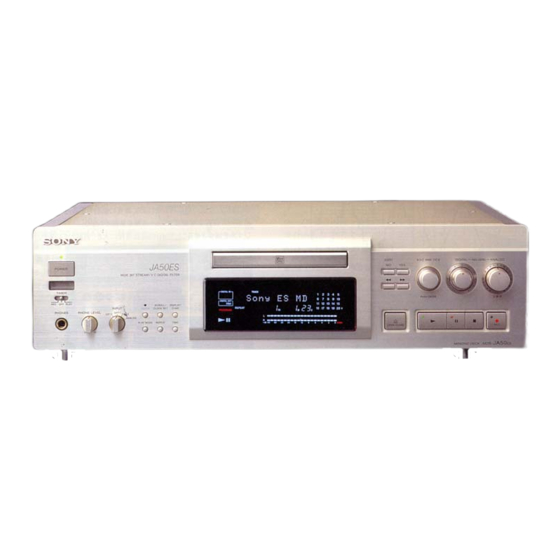
Summary of Contents for Sony MDS-JA50ES
- Page 1 MDS-JA50ES SERVICE MANUAL US Model AEP Model UK Model Photo: GOLD Model Name Using Similar Mechanism MD Mechanism Type MDM-4A Base Unit Type MBU-2B Optical Pick-up Type KMS-210A/J-N SPECIFICATIONS MINIDISC DECK MICROFILM — 1 —...
- Page 2 THE PARTS LIST ARE CRITICAL TO SAFE OPERATION. Vaihda paristo ainoastaan laitevalmistajan suosittelemaan tyyppiin. REPLACE THESE COMPONENTS WITH SONY PARTS Hävitä käytetty paristo valmistajan ohjeiden mukaisesti. WHOSE PART NUMBERS APPEAR AS SHOWN IN THIS MANUAL OR IN SUPPLEMENTS PUBLISHED BY SONY. — 2 —...
-
Page 3: Table Of Contents
TABLE OF CONTENTS The laser component in this product is capable of emitting radiation exceeding 1. SERVICING NOTE ............4 the limit for Class 1. 2. GENERAL ................7 3. DISASSEMBLY 3-1. Tray Assembly ..............26 3-2. Bracket (Motor) ASSY ............27 3-3. -
Page 4: Servicing Note
SECTION 1 SERVICING NOTE HOW TO OPEN THE DISC TRAY WHEN POWER SWITCH TURNS OFF 1 Remove the fourteen screws (BVTT 3x8) from the bottom plate. 2 Remove the bottom plate. 3 Rotate the pulley gear in the arrow direction A, and open the tray assembly in the arrow direction B. Pully gear Tray assembly FORCED RESET... - Page 5 RETRY CAUSE DISPLAY MODE • In this test mode, the causes for retry of the unit during recording can be displayed on the fluorescent display tube. This is useful for locating the faulty part of the unit. • The retry cause, number of retries, and number of retry errors are displayed. Each is displayed in hexadecimal number. Method: 1.
- Page 6 Reading the Retry Cause Display Higher Bits Lower Bits Hexa- Hexadecimal Cause of Retry Occurring conditions decimal b7 b6 b5 b4 b3 b2 b1 b0 Binary shock *1 When more than 3.5 shocks are detected When ADER was counted more than ader5 five times continuously Discontinuous address...
-
Page 7: General
SECTION 2 GENERAL Location of Parts and Controls 1 2 3 4 5 6 8 9 0 !¡ !™ @¢ @£ @™ @º !ª !• !¶ !¢ !£ !∞ @¡ !§ 1 POWER switch !º AMS knob 2 Remote sensor !¡... - Page 8 This section is extracted from instruction manual. — 8 —...
- Page 9 — 9 —...
- Page 10 — 10 —...
- Page 11 — 11 —...
- Page 12 — 12 —...
- Page 13 — 13 —...
- Page 14 — 14 —...
- Page 15 — 15 —...
- Page 16 — 16 —...
- Page 17 — 17 —...
- Page 18 — 18 —...
- Page 19 — 19 —...
- Page 20 — 20 —...
- Page 21 — 21 —...
- Page 22 — 22 —...
- Page 23 — 23 —...
- Page 24 — 24 —...
- Page 25 — 25 —...
-
Page 26: Disassembly
SECTION 3 DISASSEMBLY Note : Follow Xthe disassembly procedure in the numerical order given. 3-1. TRAY ASSEMBLY 2 Two screws (BVTP 3x6) 3 Two screws (BVTP 3x6) 1 Rotate the pulley gear in the arrow direction A , and pull out the tray 9 Shaft 4 Bracket assembly. -
Page 27: Bracket (Motor) Assy
3-2. BRACKET (MOTOR) ASSY 3 Connector (CN198 : HMOT board) 4 Bracket (Motor) assembly 1 Two screws (BVTT 3x6) 2 Two screws (BVTT 3x6) 3-3. HOLDER ASSY Slider assembly Shaft A 1 When removing, move the slider assembly in the arrow direction, and check that shaft A is at the position shown in the figure. -
Page 28: Base Unit
3-4. BASE UNIT 1 Leaf spring (UDL) 2 Leaf spring (UDR) 3 Holder assembly 5 Base unit (MBU-2B) 4 Three screws (BVTP 3x6) 3-5. HMOT BOARD AND HLIM BOARD 5 Stopper washer 6 Gear (HEAD C) 7 Stopper washer 3 Lever (OWH) 1 Stopper 4 Torsion spring (OWH) washer... -
Page 29: Test Mode
SECTION 4 TEST MODE 4-1. Setting the Test Mode While pressing the AMS knob, insert the power plug into the power supply inlet, and release the AMS knob. 4-2. Exiting the Test Mode Press the REPEAT button. Unplug the power plug from an outlet. 4-3. - Page 30 4-4-2. Operating the Continuous Recording Mode 1. Entering the continuous recording mode 1 Set the MO disc in the unit. 2 Rotate the AMS knob and display “CREC MODE”. 3 Press the YES button to change the display to “CREC IN”. 4 When access completes, the display changes to “CREC ( ”...
- Page 31 4-6. Test Mode Displays Each time the DISPLAY/CHAR button is pressed, the display changes in the following order. MODE display n Error rate display n Address display 1. MODE display Displays “TEMP ADJUS”, “CPLAY MODE”, etc. 2. Error rate display Error rates are displayed as follows.
-
Page 32: Electrical Adjustments
SECTION 5 ELECTRICAL ADJUSTMENTS Precautions for Checking Laser Diode Emission Precautions for Adjustments To check the emission of the laser diode during adjustments, never 1) When replacing the following parts, perform the adjustments and checks with ® in the order shown in the following table. view directly from the top as this may lose your eye-sight. - Page 33 Laser Power Adjustment Temperature Compensation Offset Adjustment Connection : Save the temperature data at that time in the non-volatile memory as 25 ˚C reference data. Laser power meter Note : 1. Usually, do not perform this adjustment. 2. Perform this adjustment in an ambient temperature of 22 ˚C to 28 ˚C.
- Page 34 Traverse Adjustment 11. Rotate the AMS knob until the waveform of the oscilloscope moves closer to the specified value. In this adjustment, waveform varies at intervals of approx. 3%. Connection : Adjust the waveform so that the specified value is satisfied as much as possible.
- Page 35 Focus Bias Adjustment Error Rate Check CD Error Rate Check Adjusting Method : 1. Load a continuously recorded disc (Refer to “Page 32 Creating Checking Method : Continuously Recorded Disc”.). 1. Load a check disc (MD) TDYS-1. 2. Rotate the AMS knob and display “CPLAY MODE”. 2.
- Page 36 Adjusting Points and Connecting Points [BD BOARD] (SIDE A) D101 IC191 [BD BOARD] (SIDE B) (IOP) (I + 5V) IC101 RV101 (VC) IC171 RV102 (TEO) IC121 — 36 —...
-
Page 37: Diagrams
MDS-JA50ES SECTION 6 DIAGRAMS 6-1. BLOCK DIAGRAMS — BD SECTION — DIGITAL SIGNAL PROCESSOR, FILTER DIGITAL SERVO SIGNAL PROCESSOR, DOUT EFM/ACIRC ENCODER/DECODER IC121 51 52 49 53 Q181,182 SQSY HR901 OVER WRITE OVER HEAD DIDT SUBCODE HEAD DRIVE WRITE DRIVE... -
Page 38: Digital Section
MDS-JA50ES DOUT — DIGITAL SECTION — ADIN DOUT DODT ATRAC ENCODER/DECODER SAMPLING RATE CONVERTER, DIGITAL FILTER DIGITAL AUDIO INTERFACE RECEIVER IC206 IC207 IC203 BUFFER IC210 IC205 SCTX DODT DATA DATAI DATAO DATA DIDT DATAO DATA DIN1 DECIMATION LRCK INPUT ATRAC... -
Page 39: Audio Section
MDS-JA50ES — AUDIO SECTION — L.P.F. MIX/LINE AMP D/A CONVERTER CURRENT PULSE NOISE SHAPER, DIGITAL FILTER IC509 IC510 IC502 IC505 IC501 L1(+) IN1+ IO1+ DFDTOL DATAI L1(–) IN1– IO2– DOUT DFBCKO LRCKI SWITCHING BCKI L2(+) IN2+ IO1– CONVERT CIRCUIT ABCK... -
Page 40: Circuit Boards Location
MDS-JA50ES — POWER SECTION — 6-2. CIRCUIT BOARDS LOCATION PW board T001 POWER +12V REG TRANSFORMER IC904 CN001 RY901 RECT AMP. +12V D911,912 +5V REG DIO board IC304 AC board RECT AD. +5V D909,910 +5V REG S001 IC503 RELAY MAIN... - Page 57 IC204 L88MS33T-TL START UP REFERENCE ERROR CIRCUIT VOLTAGE ON/OFF CURRENT PROTECTOR CONTROL LIMITER VOUT IC205 TC74LCX244FS (EL) IC210 TC74VHCT244F (EL) IC207 MSM9404AGS-BK 64 63 62 61 58 57 56 55 54 53 52 51 50 49 INPUT I/F (SIPO) IIR/FIR FILTER CONTROL SRDT...
- Page 58 IC206 CXD2537R SWDT SCLK ATRAC Encoder/Decoder XLAT SRDT SENS SMD0 SMD1 Memory Data Controller I/F Memory XINT RCPB XRAS WRMN ATRAC Encoder/Decoder I/F TST0 XCAS TST1 DI Block TST2 RAM R/W Controller XRST CD-ROM Encoder/Decoder TST3 TST4 Clock Generator TST5 IC302 CXD8593M-E1 AGND VREF+...
- Page 59 IC352 SN74HC153ANS-E20 IC353 SN74HCU04ANS-E20 DATA INPUTS STROBE OUTPUT SELECT STROBE 1C0 OUTPUT SELECT DATA INPUTS IC501 CXD8595Q PLMG2 NRGCLR SYSM NSDOL4 LATCH NSDOL3 SHIFT NSDOL2 NSDOL1 INIT LRCKI DATAI BCKI 64FSI NSDOR1 INVO2 NSDOR2 INVO1 NSDOR3 INVI NSDOR4 MCKIN 128FSO CKVDD PLMG1 DINIT...
- Page 60 IC502 CXD2562Q-CS 51 50 49 48 47 TIMING CIRCUIT SYNC COEF SPLM INTERPOLATER DATAOUT 18/20 ON/OFF INTERPOLATER DVDDR TEST1 VSUB (D) R TEST2 VSUB (CHIP) R THIRD ORDER TEST3 NOISE SHAPER VDD2 DVDDL VSUB (D) L R1 (–) VSUB (CHIP) L THIRD ORDER VDD2 NOISE SHAPER...
- Page 61 IC901 M62005L IC908 M5293L INTERRUPT SIGNAL – GENERATOR REFERENCE VOLTAGE RESET SIGNAL – GENERATOR REFERENCE – ON/OFF VOLTAGE OVERHEAT OVERCURRENT PROTECTION LIMITTER IC902 LA5602 V IN ERROR REFERENCE VOLTAGE OVER CURRENT LIMITTER OVER HEAT PROTECTION ON/OFF RESET CDEL V OUT IC906 SN74HC04ANS-E20 —...
-
Page 62: Ic Pin Functions
6-21. IC PIN FUNCTIONS • IC101 RF Amplifier (CXA1981AR)/BD board Pin No. Pin Name Function Middle point voltage (+2.5V) generation output Input of signal from optical pick-up detector 2 to 7 A to F F operation amplifier input F operation amplifier output Front monitor Connected to photo diode Input for setting laser power APCREF... - Page 63 • IC121 Digital Signal Processor, Digital Servo Processor, EFM/ACIRC Encoder/Decoder (CXD2535CR)/BD board Pin No. Pin Name Function FS256 11.2896 MHz clock output (MCLK) (Not used) Output of FOK signal to system controller Outputs “H” when focus is set DFCT Outputs defect ON/OFF switching signal to ATRAC encoder/decoder SHCK Outputs track jump detection signal to system controller SHCKEN...
- Page 64 Pin No. Pin Name Function WFCK clock (7.35 kHz) signal output WFCK (Playback: EFM decoder PLL Recording: EFM encoder PLL) “H”: Opens playback EFM frame sync protection window GTOP “H”: Playback EFM sync and interpolation protection timing match EFM decoder PLL clock output (98 fs=4.3218 MHz) XPLCK Falling edge and EFM signal edge match EFM signal output (Recording)
- Page 65 Pin No. Pin Name Function TEST1 Test pin (Fixed at “L”) Input of ADIP dual FM signal from RF amplifier (22.05 kHz ±1 kHz) ADFG (TTL Schmidt input) TS25 Test pin (Fixed at “L”) LDDR Laser APC signal output TRDR Tracking servo drive signal output (–) TFDR Tracking servo drive signal output (+)
- Page 66 • IC202 System Controller (M30610EC-1086FP)/DIG board Pin No. Pin Name Function Not used 1, 2 — — JOG0 AMS jog signal input JOG1 ATP address sync or sub code Q sync (SCOR) input from CXD2535CR SQSY “L” is input every 13.3 msec Mainly “H” REMOCON Remote control signal interruption input Not used...
- Page 67 Pin No. Pin Name Function SRC TEST The second reset signal output from sampling rate converter 46 to 48 — — Not used DAMUTE D/A line mute output “L”:Active Strobe signal output to power supply circuit When power is ON:“H”, When standby:“L” OUTSW Detection input from loading out detection switch INSW...
- Page 68 Pin No. Pin Name Function CSET0 Destination setting pin CSET1 POWER POWER LED drive output PLAY PLAY (() LED drive output — — Not used REC (r) LED drive output — — Not used PAUSE PAUSE (P) LED drive output —...
- Page 69 • IC203 Digital Audio Interface Receiver (LC89051V-TLM)/DIG board Pin No. Pin Name Function DIN1 Data input with built-in amplifier (responding to the coaxial optical module) DIN2 Data input (responding to the optical module) (Not used) E/DOUT Emphasis, input bi-phase, validity flag output (Not used) —...
- Page 70 • IC206 Shock-Proof Memory Controller, ATRAC Encoder/Decoder (CXD2537R)/DIG board Pin No. Pin Name Function Power supply (+5V) — SWDT Input of write data signal from system controller Input of serial clock signal from system controller XLAT Input of serial latch signal from system controller Output of read data signal to system controller SRDT Internal status (SENSE) output (Not used)
- Page 71 Pin No. Pin Name Function 48, 49 Address signal output (Not used) A11, A10 — Ground — Power supply (+5V) 52 to 55 Address signal output A03 to A00 56 to 60 Address signal output A04 to A08 Output enable control signal output Column address strobe signal output XCAS —...
- Page 72 • IC207 Sampling Rate Converter, Digital Filter (MSM9404AGS-BX)/DIG board Pin No. Pin Name Function Data output (Not used) Data select control input “L”:DI0 n DO, “H”:DI1 n DO (Fixed at “L”) SRDT Serial data output SWDT Serial data input Serial clock input XLAT Serial latch pulse input INIT...
- Page 73 Pin No. Pin Name Function — Not used DAOR Rch D/A 8Fso, 4Fso data output (Not used) DAOL Lch D/A 8Fso, 4Fso data output (Not used) TEST3 Test pin (Fixed at “L”) DEMP Deemphasis setting input “L”:OFF (Fixed at “L”) Deemphasis setting input Fsi frequency selection input (Fixed at “L”) 48 to 50 TB3 to TB1...
- Page 74 • IC301 Digital Filter (CXD8512Q)/AD board Pin No. Pin Name Function TEST Test pin (Fixed at “L”) — Not used SYNC Sync mode selection (Fixed at “L”) INIT Initialization input — Not used CFLG Flag output for calibration (Not used) 7, 8 —...
- Page 75 Pin No. Function Pin Name Not used — Test pin (Fixed at “L”) OSEL Output data word length selection “H”: 24 bits, “L”: 16 bits (Fixed at “H”) OBIT Rch data output (Not used) Lch data output Not used — Ground 52, 53 —...
- Page 76 • IC501 Noise Shaper, Digital Filter (CXD8595Q)/DA board Pin No. Pin Name Function PLMG2 4 bit conversion data setting pin in SCD mode (Fixed at “L”) — Power supply (+5V) Noise shaping data Lch parallel output 4 (MSB) (Not used) NSDOL4 Noise shaping data Lch parallel output 3 (4SB) (Not used) NSDOL3...
- Page 77 Pin No. Pin Name Function — Ground 41, 42 Bit clock input BCKI Data input DATAI LR clock input LRCKI Initialize input “L”:Reset INIT Serial data input Serial shift clock input SHIFT Serial latch clock input LATCH External mute signal input “H”:Active (Fixed at “L”) SYSM N/S calculation section register clear signal input “H”:Active (Fixed at “L”) NRGCLR...
-
Page 78: Exploded Views
SECTION 7 EXPLODED VIEWS NOTE: • -XX, -X mean standardized parts, so they may have • The mechanical parts with no reference number in The components identified by mark ! some difference from the original one. the exploded views are not supplied. or dotted line with mark ! are critical •... -
Page 79: Chassis Section
7-2. CHASSIS SECTION T001 supplied not supplied not supplied T002 not supplied not supplied 63 72 not supplied not supplied not supplied The components identified by mark ! or dotted line with mark ! are critical not supplied for safety. Replace only with part number speci- fied. -
Page 80: Front Panel Section 1
7-3. FRONT PANEL SECTION 1 Supplied with S701 FL701 not supplied not supplied Ref. No. Part No. Description Remark Ref. No. Part No. Description Remark 4-987-518-01 FILTER 1-777-736-11 WIRE (FLAT TYPE)(26 CORE) * 102 A-4699-460-A PSW BOARD, COMPLETE * 108 4-972-608-01 HOLDER (DIA. -
Page 81: Front Panel Section 2
4-987-494-11 PANEL, FRONT (BLACK)(AEP,UK,G) * 171 4-987-515-11 GUIDE (INPUT)(BLACK) 4-987-494-21 PANEL, FRONT (BLACK)(US) * 172 4-987-513-01 GUIDE (FUNC) 4-942-568-01 EMBLEM (NO.5), SONY (BLACK) 4-942-568-31 EMBLEM (NO.5), SONY (GOLD) * 173 A-4699-461-A HP BOARD, COMPLETE 4-987-522-01 BUTTON (FUNC)(GOLD) * 159 4-987-535-01 GUIDE (AMS)(GOLD) -
Page 82: Mechanism Section 1 (Mdm-4A)
7-5. MECHANISM SECTION 1 (MDM-4A) not supplied Ref. No. Part No. Description Remark Ref. No. Part No. Description Remark * 301 4-987-291-01 BRACKET (TOP) * 308 4-987-294-01 GUIDE (SHAFT) 4-987-293-01 GEAR (4) 4-987-271-01 STOPPER (SHAFT B) * 303 X-4947-820-1 SLIDER (D) ASSY 4-987-269-01 RACK (L) * 304 4-987-267-01 TABLE (EJECT) -
Page 83: Mechanism Section 2 (Mdm-4A)
7-6. MECHANISM SECTION 2 (MDM-4A) M191 Ref. No. Part No. Description Remark Ref. No. Part No. Description Remark * 351 X-4947-819-1 SLIDER ASSY * 361 X-4947-823-1 BRACKET (MOTOR) ASSY X-4947-937-1 LEVER (LOCK) ASSY 4-987-274-01 TABLE (LOADING) * 353 X-4947-818-1 CHASSIS ASSY 4-968-919-31 WASHER, STOPPER * 354 1-663-898-11 OUT BOARD... -
Page 84: Mechanism Section 3 (Mdm-4A)
7-7. MECHANISM SECTION 3 (MDM-4A) 404 405 not supplied MBU-2B M192 Ref. No. Part No. Description Remark Ref. No. Part No. Description Remark 4-987-273-01 SPRING (UDL), LEAF 4-987-272-01 SPRING (UDR), LEAF * 402 X-4947-847-1 HOLDER ASSY * 410 1-663-896-11 HLIM BOARD 4-989-938-01 WASHER, STOPPER 4-968-919-31 WASHER, STOPPER * 411... -
Page 85: Base Unit Section (Mbu-2B)
7-8. BASE UNIT SECTION (MBU-2B) S102 HR901 not supplied supplied M102 supplied M101 The components identified by mark ! or dotted line with mark ! are critical for safety. Replace only with part number speci- fied. Ref. No. Part No. Description Remark Ref. -
Page 86: Electrical Parts List
SECTION 8 ELECTRICAL PARTS LIST Note: • Due to standardization, replacements in the parts list • SEMICONDUCTORS The components identified by mark ! may be different from the parts specified in the In each case, u: µ , for example: or dotted line with mark ! are critical diagrams or the components used on the set. - Page 87 AVOL Ref. No. Part No. Description Remark Ref. No. Part No. Description Remark IC306 8-759-712-02 IC NJM2114D A-4673-809-A BD BOARD, COMPLETE IC307 8-759-712-02 IC NJM2114D ******************* IC308 8-759-712-02 IC NJM2114D < CAPACITOR > < COIL > C101 1-104-913-11 TANTAL. CHIP 10uF L301 1-408-405-00 INDUCTOR...
- Page 88 Ref. No. Part No. Description Remark Ref. No. Part No. Description Remark C182 1-163-038-91 CERAMIC CHIP 0.1uF Q151 8-729-905-18 TRANSISTOR DTC144EU Q162 8-729-101-07 TRANSISTOR 2SB798-DL C183 1-163-038-91 CERAMIC CHIP 0.1uF Q163 8-729-905-12 TRANSISTOR DTA144EU C184 1-107-836-11 ELECT CHIP 22uF Q164 8-729-924-19 TRANSISTOR DTA123JU C185 1-164-611-11 CERAMIC CHIP...
- Page 89 Ref. No. Part No. Description Remark Ref. No. Part No. Description Remark R169 1-219-724-11 METAL CHIP 1/4W C530 1-164-159-11 CERAMIC 0.1uF R170 1-216-073-00 METAL CHIP 1/10W R171 1-216-073-00 METAL CHIP 1/10W C531 1-124-721-11 ELECT 10uF R172 1-216-065-00 METAL CHIP 4.7K 1/10W C532 1-164-159-11 CERAMIC...
- Page 90 Ref. No. Part No. Description Remark Ref. No. Part No. Description Remark C595 1-164-159-11 CERAMIC 0.1uF R505 1-259-380-11 CARBON 1/6W < CONNECTOR > R506 1-259-380-11 CARBON 1/6W R507 1-259-380-11 CARBON 1/6W CN501 1-573-150-11 SOCKET, CONNECTOR 18P R508 1-259-404-11 CARBON 1/6W * CN503 1-564-514-11 PLUG, CONNECTOR 11P R509...
- Page 91 Ref. No. Part No. Description Remark Ref. No. Part No. Description Remark R572 1-249-616-11 CARBON 470K 1/4W C231 1-126-193-11 ELECT R573 1-259-500-11 CARBON 1/6W R574 1-259-500-11 CARBON 1/6W C232 1-163-038-91 CERAMIC CHIP 0.1uF R575 1-249-616-11 CARBON 470K 1/4W C233 1-163-038-91 CERAMIC CHIP 0.1uF C234 1-126-206-11 ELECT CHIP...
- Page 92 Ref. No. Part No. Description Remark Ref. No. Part No. Description Remark IC207 8-759-461-47 IC MSM9404AGS-BK R235 1-216-073-00 METAL CHIP 1/10W IC208 8-759-344-86 IC MSM514400C-70SJ R236 1-216-065-00 METAL CHIP 4.7K 1/10W IC210 8-759-272-05 IC TC74VHCT244F(EL) R237 1-216-109-00 METAL CHIP 330K 1/10W IC211 8-759-031-84 IC SC7S04F...
- Page 93 DISP Ref. No. Part No. Description Remark Ref. No. Part No. Description Remark < VIBRATOR > R361 1-259-404-11 CARBON 1/6W R363 1-259-404-11 CARBON 1/6W X201 1-767-273-11 VIBRATOR, CERAMIC (CHIP TYPE)(10MHz) R364 1-259-404-11 CARBON 1/6W X202 1-760-458-21 VIBRATOR, CRYSTAL (32.768kHz) R365 1-259-401-11 CARBON 1/6W R366...
- Page 94 DISP DVOL HLIM HMOT Ref. No. Part No. Description Remark Ref. No. Part No. Description Remark R723 1-259-464-11 CARBON 1/6W 1-663-899-11 HMOT BOARD R724 1-259-452-11 CARBON 1/6W *********** R725 1-259-444-11 CARBON 4.7K 1/6W < MOTOR > R726 1-259-440-11 CARBON 3.3K 1/6W R727 1-259-436-11 CARBON...
- Page 95 LMOT Ref. No. Part No. Description Remark Ref. No. Part No. Description Remark < VARIABLE RESISTOR > A-4699-460-A PSW BOARD, COMPLETE ******************** RV651 1-225-372-11 RES, VAR, CARBON 20K/20K (PHONE LEVEL) 4-972-608-01 HOLDER (DIA. 5), LED 4-976-360-02 REINFORCEMENT (CONT) ************************************************************** 1-663-897-11 IN BOARD <...
- Page 96 Ref. No. Part No. Description Remark Ref. No. Part No. Description Remark A-4699-455-A PW BOARD, COMPLETE (US) * CN905 1-564-704-11 PIN, CONNECTOR (SMALL TYPE) 2P *********************** < DIODE > A-4699-591-A PW BOARD, COMPLETE (AEP,UK,G) ***************************** D901 8-719-987-63 DIODE 1N4148M D902 8-719-987-63 DIODE 1N4148M 3-309-144-21 HEAT SINK D903...
- Page 97 Ref. No. Part No. Description Remark Ref. No. Part No. Description Remark < TRANSISTOR > ACCESSORIES & PACKING MATERIALS ******************************* Q901 8-729-038-19 TRANSISTOR RT1P144S-TP Q902 8-729-038-19 TRANSISTOR RT1P144S-TP 1-475-091-11 REMOTE COMMANDER (RM-D13M) Q903 8-729-422-57 TRANSISTOR UN4111 1-590-925-31 CORD, CONNECTION (AUDIO, 100cm) Q905 8-729-140-98 TRANSISTOR 2SD773-34 3-859-239-11 MANUAL, INSTRUCTION (ENGLISH,FRENCH)
- Page 98 MDS-JA50ES Sony Corporation 97B0973-1 9-960-837-11 Printed in Japan © 1997. 2 Home A&V Products Company Published by Service and Safety Engineering Dept. (Shibaura) — 120 —...