Advertisement
Quick Links
Chipsmall Limited consists of a professional team with an average of over 10 year of expertise in the distribution
of electronic components. Based in Hongkong, we have already established firm and mutual-benefit business
relationships with customers from,Europe,America and south Asia,supplying obsolete and hard-to-find components
to meet their specific needs.
With the principle of "Quality Parts,Customers Priority,Honest Operation,and Considerate Service",our business
mainly focus on the distribution of electronic components. Line cards we deal with include
Microchip,ALPS,ROHM,Xilinx,Pulse,ON,Everlight and Freescale. Main products comprise
IC,Modules,Potentiometer,IC Socket,Relay,Connector.Our parts cover such applications as commercial,industrial,
and automotives areas.
We are looking forward to setting up business relationship with you and hope to provide you with the best service
and solution. Let us make a better world for our industry!
Contact us
Tel: +86-755-8981 8866 Fax: +86-755-8427 6832
Email & Skype: info@chipsmall.com Web: www.chipsmall.com
Address: A1208, Overseas Decoration Building, #122 Zhenhua RD., Futian, Shenzhen, China
Advertisement

Related Manuals for Toshiba TC78B002FNG


Summary of Contents for Toshiba TC78B002FNG
- Page 1 Chipsmall Limited consists of a professional team with an average of over 10 year of expertise in the distribution of electronic components. Based in Hongkong, we have already established firm and mutual-benefit business relationships with customers from,Europe,America and south Asia,supplying obsolete and hard-to-find components to meet their specific needs.
- Page 2 TOSHIBA CMOS Integrated Circuit Silicon Monolithic TC78B002FNG Single Phase Full-wave Driver for Fan Motor TC78B002FNG is a single phase full-wave driver for fan motor. It TC78B002FNG has a DMOS device in an output transistor. A highly effective drive is possible by adopting a DMOS output driver with low ON resistance and a PWM drive system.
- Page 3 TC78B002FNG Block Diagram (Application circuit) VREG 5V Regulator Hall Ele. OUT1 VSOFT Driver VOFF OUT2 Control Logic 7bit OSCR Lock Protection 2013-10-17...
-
Page 4: Table Of Contents
TC78B002FNG Pin Assignment VREG VSOFT OSCR VOFF OUT1 OUT2 2013-10-17... -
Page 5: Vreg
TC78B002FNG Pin Description Pin No. Pin name Description VREG Output pin for reference voltage of 5 V Hall signal input pin + Hall signal input pin- OSCR Connection pin for resistor of oscillation circuit Output pin for lock detection OUT1... - Page 6 TC78B002FNG Absolute Maximum Ratings (Ta = 25°C) Characteristics Symbol Rating Unit Power supply voltage Input voltage -0.3~6 (Note 1) Output voltage (Note 2) OUT1,OUT2 (Note 3) Output current VREG FG pin sink current RDO pin sink current Power dissipation 0.96...
- Page 7 TC78B002FNG Electrical Characteristics (Ta = 25°C and VM = 12 V, unless otherwise specified.) Characteristics Symbol Test conditions Typ. Unit VM = 12 V, V = OPEN Power supply current Hall input=100Hz, output OPEN Common mode input voltage ...
-
Page 8: Rdo
TC78B002FNG Characteristics Symbol Test conditions Typ. Unit Output low voltage =5mA FG/RDO μA Output leakage current FG/RDO Current limit detecting voltage for RS pin 0.27 0.33 μs Masking time of current limit detection (Design target value) (Note 1) mask ... - Page 9 TC78B002FNG Reference Data 125℃ 25℃ 125℃ -40℃ 25℃ -40℃ -40℃ 25℃ 125℃ Operation Voltage Range Operation Voltage Range Supply voltage. VM[V] Supply voltage. VM[V] Fig.1 Power supply current Fig.2 Hall input Hysteresis voltage -40℃ 25℃ 125℃ 3.5V Output Current. I [mA] Output Current.
- Page 10 TC78B002FNG 125℃ 3.5V 25℃ -40℃ Output Current. I [mA] Output Current. I [mA] FG/RDO FG/RDO Fig.8 FG/RDO pin Output low voltage (Ta=25℃) Fig.7 FG/RDO pin Output low voltage (VM=12V) 0.32 125℃ 0.31 25℃ 125℃ 25℃ -40℃ -40℃ 0.29 Operation Voltage Range Operation Voltage Range 0.28...
- Page 11 TC78B002FNG I/O Equivalent Circuits Pin name I/O signal Equivalent circuit Hall signal input pin VREG VREG In-phase input voltage range 0V to V -1.5V Control voltage input pin VSOFT Control voltage input pin VREG VOFF VSOFT VOFF VREG Voltage output pin...
-
Page 12: Out1
TC78B002FNG Pin name I/O signal Equivalent circuit Motor output pin OUT1 OUT2 OUT1 OUT2 0.3V OSCR VREG VREG Connection pin for resistor of oscillation circuit OSCR 2013-10-17... - Page 13 TC78B002FNG Functional Description The equivalent circuit diagrams may be simplified or some parts of them may be omitted for explanatory purposes. Timing charts may be simplified for explanatory purposes. Basic Operation At startup, the motor is driven by a square-wave drive by determining the conducting phase with hall input signal.
-
Page 14: Gnd
TC78B002FNG Timing chart (Lock protection) HP-HM OUT1 OFF (Hi-Z) OFF (Hi-Z) OUT2 VSP/ VMI Input Pin Output starts when VSP pin at the voltage of more than V . And it turns off at the voltage of V or less. - Page 15 TC78B002FNG OSC Frequency and PWM Frequency Oscillation frequency is approximated by below formula. = 1/(2C[F]×R [Ω]) [Hz]= 1/(2×2.08e-12[F]×R [Ω]) [Hz] Oscillation frequency f is 10MHz(typ) when external resistor ROSC is 24kΩ PWM frequency f /400. PWM Output Drive In PWM drive, upper power transistor is turned on and off repeatedly.
- Page 16 TC78B002FNG 7. Turning Off Output turns off when the voltage of VSP pin is V or less. AD(L) Before all output power transistors are turned off, the time, until the edge of FG signal is detected twice or the frequency of 5 Hz or less is detected, is defined PWM OFF term.
- Page 17 TC78B002FNG 8. Soft Switching Soft switching is performed by changing the output PWM duty gradually when conducting phase switches. The time of soft switching is determined by the voltage of VSOFT pin and that of VOFF pin. HP-PM HP-PM OUT1...
- Page 18 TC78B002FNG <Relation between the voltage of VSOFT pin and the term of soft switching> → 0° VSOFT = 0V → 87.2° (In case voltage of V VSOFT = V or more is input, it is set to 87.2°.) VSOFT Term...
- Page 19 TC78B002FNG < Relation between the voltage of VOFF pin and the term of turning off> → 0° VOFF = 0V → 87.2° (In case voltage of V VOFF = V or more is input, it is set to 87.2°) VOFF...
- Page 20 TC78B002FNG <PWM change during soft switching> Soft switching after conducting phase switch: It changes gradually from 4% to 100% of output PWM duty determined by the voltage of VSP pin. Its number of steps is 16 in maximum. Soft switching before conducting phase switch: It changes gradually from 100% to 4% of output PWM duty determined by the voltage of VSP pin.
- Page 21 TC78B002FNG Lead Angle Lead angle of the conducting signal can be set in the range of 0 to 22.5° against the hall signal. Lead angle is set by analog input of LA pin (The range of 0 to V is divided into 32 steps and lower 17 steps are used.)
- Page 22 TC78B002FNG 10. Lock protection It monitors the motor rotation by the hall signal and operates when the zero cross of the hall signal can not be detected for certain time (T ) or more. When lock protection operates, the upper output transistor is turned off for 1ms(typ) and then all output power transistors are turned off.
- Page 23 TC78B002FNG 12. Current Limit This function operates when the output voltage reaches the current limit detection voltage (V = 0.3 V (typ)). It is detected by the resistor R Current value which over current Over current detection voltage (V protection operates (I...
- Page 24 TC78B002FNG 13. Over Current Protection (ISD) Detection of current of the output power transistor is incorporated. Each current flowing through four power transistors is detected individually. When the current exceeds the detection value, the related output power transistor is turned off. Then all output power transistors are turned off 1ms(typ) after this related output power transistor is turned off.
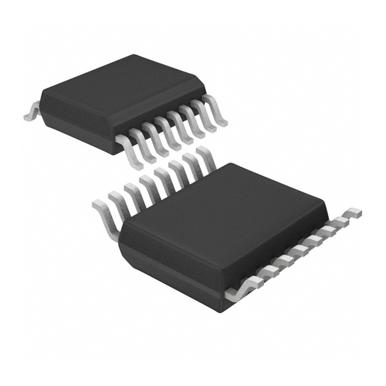
- Page 25 TC78B002FNG Package Dimensions SSOP16-P-225-0.65B Unit: mm 2013-10-17...
- Page 26 The application circuits shown in this document are provided for reference purposes only. Thorough evaluation is required, especially at the mass production design stage. Toshiba does not grant any license to any industrial property rights by providing these examples of application circuits. 5. Test Circuits Components in the test circuits are used only to obtain and confirm the device characteristics.