
Related Manuals for Panasonic KX-TDA0187


Summary of Contents for Panasonic KX-TDA0187
- Page 1 ORDER NO. KMS0308824C1 T-1 Trunk Card KX-TDA0187 (for U.S.A.) 2003 Panasonic Communications Co., Ltd. All rights reserved. Unauthorized copying and distribution is a violation of law.
- Page 2 IMPORTANT INFORMATION ABOUT LEAD FREE, (PbF), SOLDERING If lead free solder was used in the manufacture of this product the printed circuit boards will be marked PbF, Standard laded, (Pb), solder can be used as usual on boards without the PbF mark. When this mark does appear please read and follow the special instructions described in this manual on the use of PbF and how it might be permissible to use Pb solder during service and repair work.
- Page 3 We will use PbF solder when discussing the lead free solder used in our manufacturing process which is made from Tin, (Sn), Silver, (Ag), and Copper, (Cu). This model, and others like it, manufactured using lead free solder will have PbF stamped on the PCB.
- Page 4 1.2. HOW TO RECOGNIZE THAT Pb FREE SOLDER IS USED 2. FOR SERVICE TECHNICIANS ICs and LSIs are vulnerable to static electricity. When repairing, the following precautions will help prevent recurring malfunctions. 1. Cover the plastic part's boxes with aluminum foil. 2.
- Page 5 4. NAMES AND LOCATIONS Overview Inside View...
- Page 6 Note: *Null slot is not available for any optional service cards. 4.1. INSTALLING/REMOVING THE OPTIONAL SERVICE CARDS Slot Condition Card Type Slot Type Option Slot MPR Slot KX-TDA100:Free Slots 1 to 5 KX-TDA200:Free Slots 1 to 10 MPR Card CO Line Cards Extension Cards OPB3 Card CTI-LINK Card...
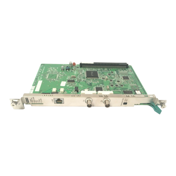
- Page 7 Accessory and User-supplied Items Accessory (included): ferrite core x 1 User-supplied (not included): RJ45 connector Notes - Connect this optional service card to the CO line through NT1; do not connect to the CO line directly. - T1 Card must be installed behind an FCC registered and UL or CSA- NRTL listed CSU.
- Page 8 Signal Name Level [V] Function Receive data (+) Receive data (-) Reserved Transmit data (-) Transmit data (+) Reserved LED Indications Indication Color Description CARD STATUS Green/Red OFF: Power Off Green ON: Normal (all ports are idle) Green Flash (60 times per minute): Normal (a port is in use) Red ON: Fault (includes reset) Red Flash (60 times per minute): Out of Service SYNC-ERR...
- Page 9 - The Hybrid IP-PBX will continue to be powered even if the power switch is turned "OFF". - The power supply cord is used as the main disconnect device, ensure that the socket-outlet is located/installed near the equipment and is easily accessible. 1.
- Page 10 LED Indications Indication Color Description Green OFF: Power Off (includes normal reset) ON: Power On and running (on-line) Flash (60 times per minute): Power On and starting Flash (120 times per minute): Power On and resetting before system clear ALARM OFF: Normal ON: Alarm (CPU stop, alarm for each card) Flash: Alarm (MPR file error in restarting)
- Page 11 Operation 1. If the Hybrid IP-PBX does not operate properly: A. Make sure that the System Clear Switch is set to the "NORMAL" position. B. Press the Reset Button. 2. If the Hybrid IP-PBX still does not operate properly: A. Set the System Clear Switch to the "SYSTEM INITIALIZE" position.
- Page 12 1. Insert the card along the guide rails. 2. Holding the card as follows, push the release lever in the direction of the arrow so that the card is made to engage with the connector on the back board securely. 3.
- Page 13 5. TROUBLESHOOTING GUIDE...
- Page 17 6. BLOCK DIAGRAM 7. CIRCUIT OPERATION 7.1. CPU PERIPHERAL FUNCTION The CPU (IC1) is a single chip microcomputer of RISC architecture. This item describes a memory interface (program & work) and peripheral functions. 7.1.1. Memory (Program & Work) Table.5.1 List of the memory (program & work) Part Name Size Purpose...
- Page 18 7.1.2. Chip Select Logic Table.5.2 Table of Chip Select Terminals Terminals Function Remarks Wait Function used Individual Individual (Numeral is no. of Terminals Output (1) Output (2) clocks.) nCS0 (area nCS0 1+Programable or 1+ Used for Flash memory Programable+WAIT Terminals nCS1 (area nCASH nCS1...
- Page 19 7.1.3. Interrupt Fig.5.1 External interrupt image Note: - nHALT signal is consistent with the existing PBX and performs polling by I/O port. However, when the CPU (IC1) goes to Sleep Mode at HALT, the CPU (IC1) is enabled for interruption on release nHALT and return from Sleep Mode.
- Page 20 (The configuration with the interruption processing is to give a consistency with the existing PBX.) - Since the nRxMF signal of the T1-IC (IC302) occurs in periodic frame timing, the polling by i/o port is impossible. 7.2. LINE INTERFACE FUNCTION 7.2.1.
- Page 21 7.2.2. Line Interface Loopback This card has a relay for loopback test on the primary side of the line to cut and divide into the line failure or the PBX's own failure, when there is a defect in operation. Fig.5.3 Outline diagram of the line interface 7.3.
- Page 22 McBSP(Multi-Channel Buffered Serial Port) and the control system is connected with the CPU (IC1) local bus through the HPI-8 (Host Port Interface) of the DSP (IC303). See the DSP (IC303) Data Sheet for the detailed specifications of the McBSP and the HPI-8. Fig.
- Page 23 7.4. LOCAL HIGHWAY INTERFACE FUNCTION This card has the local highway in the speed of 2.048Mbps and local TSW (ASIC (IC2) internal module) to switch from the call channel (Bch) extracted from T1 line by the T1-IC (IC302), to H.100 interface. As the switching function inside the DSP (IC303) is used for the in-band signaling detection by the DSP (IC303), there is no assignment directly on the local highway map, but the operation is synchronized with the local highway in timing.
- Page 24 7.5. EC BUS INTERFACE 7.5.1. Dual Port RAM (DPRAM) Communication This card transmits and receives data between CPU (IC1) and MPR (EC bus) in a dual port RAM communication basically. Fig.5.7 shows the diagrammic illustration. Fig.5.7 DPRAM Communication diagrammic illustration...
- Page 25 7.6. OUTLINE OF RESET SYSTEM 7.6.1. Reset Operation A reset to CPU (IC1) (and the device under the control of CPU (IC1)) in this card is dominant in a reset from the main frame (MPR), and normally it is only available for software command reset or hardware reset using ASIC (IC2) from MPR.
- Page 26 Reset Type The way of Reset Specification Reset to ASIC (IC2) OR condition of the following Reset L active Power on reset Reset by the reset IC Over 10msec Reset IC specifications Power Supply voltage : 5V Reset voltage : 4.5V Reset delay time : 50msec Hardware reset from the Reset by EC_RST...
- Page 28 7.7. POWER SUPPLY This card is supplied +15V power through the backboard connector (90pin) from the power supply unit. The +15V power supply generates +5V, +3.3V and +1.8V via DC/DC converter, and they are fed as the power of circuit in the card. The +40V power supply is not used due to no feeding to the line.
- Page 29 8. IC DATA 8.1. IC1 (CPU)
- Page 30 Port Pin Terminals I/O Description nIRQ3 Reserve (interrupt) nIRQ2 T1_IC(IC302) interrupt nIRQ1 Interrupt for SAMSON (ASIC) (mainly DPRAM communication interrupt for MPR) nIRQ0 DC power down recovery detection inversion signal of (IC1) inversion signal (L:recovery) PA11 UART port for request to send [RTS0] (RS232C) PA10 UART port for clear to send [CTS0] (RS232C) Reserve (general-purpose i/o)
- Page 32 Port Pin Terminals I/O Descriptions PO[7] H/L Reserve (Jumper setup) PO[6] H/L Reserve (Jumper setup) PO[5] H/L Reserve (Jumper setup) PO[4] H/L Hardware version control bit2 (Jumper setup) PO[3] H/L Hardware version control bit1 (Jumper setup) PO[2] H/L Hardware version control bit0 (Jumper setup) PO[1] H/L Number of lines info bit1 (Jumper setup) PO[0]...
- Page 33 Port Pin Terminals I/O Descriptions P4[7] Reserve P4[6] Reserve P4[5] Reserve P4[4] Reserve P4[3] Reserve P4[2] Reserve P4[1] Reserve P4[0] Reserve P5[7] Reserve P5[6] Reserve P5[5] Reserve P5[4] Reserve P5[3] Reserve P5[2] Reserve P5[1] Reserve P5[0] Reserve 9. HOW TO REPLACE A FLAT PACKAGE IC 9.1.
- Page 34 Be certain each pin is located over the correct pad on the PCB. 2. Apply flux to all of the pins on the IC. 3. Being careful to not unsolder the tack points, slide the soldering iron along the tips of the pins while feeding enough solder to the tip so that it flows under the pins as they are heated.
- Page 35 DIODES 11. CABINET AND ELECTRICAL PARTS LOCATION...
- Page 36 12. ACCESSORIES AND PACKING MATERIALS...
- Page 38 13. REPLACEMENT PARTS LIST 1. RTL (Retention Time Limited) Note : The marking (RTL) indicates that the Retention Time is limited for this item. After the discontinuation of this assembly in production, the item will continue to be available for a specific period of time. The retention period of availability is depends on the type of assembly, and in accordance with the laws governing parts and product retention.
- Page 39 13.1. CABINET AND ELECTRICAL PARTS LOCATION Ref. No. Part No. Part Name & Description Remarks PQDF996Z SHAFT PQHR10005Z SPACER PQUB14Z2 LEVER PSHD1088Z SCREW PSMH1218Y ANGLE PSHR1238Z SPACER PSUS1020Z TORSION SPRING PSUS1021Y TORSION SPRING XUC25VW RETAINING RING 13.2. ACCESSORIES AND PACKING MATERIALS Ref.
- Page 40 Ref. No. Part No. Part Name & Description Remarks (ICS) PFVI7020VX12 C1CB00001430 C3BBKG000060 IC PSWITDA0187X PSVIPST596CN C1CB00001497 IC20 PSVISNLV74AP IC21 C0JBAZ001610 IC22 C0JBAZ001401 IC23 C0JBAB000507 IC24 PSVITC7VC32T IC26 C0JBAZ001704 IC28 PFVITC74V00T IC29 C0JBAB000504 IC30 PSVISNLV74AP IC31 PSVITC7VC32T IC302 PSVIMT9074AL IC303 PSVI320V542P IC304 C1CB00001181...
- Page 41 Ref. No. Part No. Part Name & Description Remarks L503 G0C680KA0052 COIL (CONNECTORS) K1KA90B00008 CONNECTOR PSJP07A44Z CONNECTOR (JACKS) PSJJ1T002Z JACK (CRYSTAL OSCILLATIONS) PSVCC0025GT CRYSTAL OSCILLATOR H0J200500030 CRYSTAL OSCILLATOR H0J100500018 CRYSTAL OSCILLATOR (FUSE) K5H502Z00003 FUSE IP501 K5H751Z00003 FUSE IP502 K5H751Z00003 FUSE (VARISTORS) SA301 PFRZRA311P6T VARISTOR (SURGE ABSORBER)
- Page 42 Ref. No. Part No. Part Name & Description Remarks PFVF1B221SB CERAMIC FILTER PFVF1B221SB CERAMIC FILTER PFVF1B221SB CERAMIC FILTER PFVF1B221SB CERAMIC FILTER PFVF1B221SB CERAMIC FILTER PFVF1B221SB CERAMIC FILTER PFVF1B221SB CERAMIC FILTER PFVF1B221SB CERAMIC FILTER PFVF1B221SB CERAMIC FILTER PFVF1B221SB CERAMIC FILTER PFVF1B221SB CERAMIC FILTER PFVF1B221SB CERAMIC FILTER...
- Page 43 Ref. No. Part No. Part Name & Description Remarks PFVF1B221SB CERAMIC FILTER PFVF1B221SB CERAMIC FILTER PFVF1B221SB CERAMIC FILTER PFVF1B221SB CERAMIC FILTER PFVF1B221SB CERAMIC FILTER PFVF1B221SB CERAMIC FILTER PFVF1B221SB CERAMIC FILTER PFVF1B221SB CERAMIC FILTER PFVF1B221SB CERAMIC FILTER PFVF1B221SB CERAMIC FILTER L303 PFVF1B221SB CERAMIC FILTER L304...
- Page 44 RA305 EXB38V220JV RESISTOR ARRAY, 22...
- Page 45 Ref. No. Part No. Part Name & Description Remarks (RESISTOR ) ERJ3GEY0R00 ERJ3GEY0R00 ERJ3GEY0R00 ERJ3GEY0R00 ERJ3GEY0R00 ERJ3GEY0R00 ERJ3GEY0R00 ERJ3GEY0R00 ERJ3GEY0R00 ERJ3GEY0R00 J301 ERJ3GEY0R00 J302 ERJ3GEY0R00 J323 PQ4R18XJ000 J324 PQ4R18XJ000 ERJ3GEY0R00 PQ4R10XJ000 PQ4R10XJ000 PQ4R10XJ000 PQ4R10XJ000 PQ4R10XJ000 PQ4R10XJ000 PQ4R10XJ000 PQ4R10XJ000 PQ4R10XJ000 PQ4R10XJ000 L301 ERJ3GEY0R00 L308...
- Page 46 Ref. No. Part No. Part Name & Description Remarks ERJ3GEYJ101 ERJ3GEYJ220 ERJ3GEYJ151 ERJ3GEYJ151 ERJ3GEYJ101 ERJ3GEYJ680 ERJ3GEYJ151 ERJ3GEYJ103 ERJ3GEYJ103 ERJ3GEYJ103 ERJ3GEYJ103 ERJ3GEYJ680 ERJ3GEYJ220 ERJ3GEYJ151 ERJ3GEYJ151 ERJ3GEYJ220 ERJ3GEYJ220 ERJ3GEYJ151 ERJ3GEYJ151 ERJ3GEYJ220 ERJ3GEYJ151 ERJ3GEYJ151 ERJ3GEYJ102 ERJ3GEYJ102 ERJ3GEYJ102 ERJ3GEYJ102 ERJ3GEYJ102 ERJ3GEYJ102 ERJ3GEYJ102 ERJ3GEYJ102 ERJ3GEYJ102 ERJ3GEYJ220 ERJ3GEY0R00 ERJ3GEYJ103...
- Page 47 Ref. No. Part No. Part Name & Description Remarks R107 ERJ3GEYJ103 R110 ERJ3GEYJ470 R111 ERJ3GEYJ470 R112 ERJ3GEYJ470 R113 ERJ3GEYJ470 R114 ERJ3GEYJ102 R116 ERJ3GEYJ470 R117 ERJ3GEYJ103 R118 ERJ3GEYJ103 R119 ERJ3GEYJ103 R122 ERJ3GEYJ103 R123 ERJ3GEYJ220 R124 ERJ3GEYJ220 R125 ERJ3GEYJ220 R126 ERJ3GEYJ220 R127 ERJ3GEYJ220 R128 ERJ3GEYJ221...
- Page 48 Ref. No. Part No. Part Name & Description Remarks R168 ERJ3GEYJ470 R169 ERJ3GEYJ470 R170 ERJ3GEYJ470 R171 ERJ3GEYJ470 R172 ERJ3GEYJ470 R173 ERJ3GEYJ470 R174 ERJ3GEYJ470 R175 ERJ3GEYJ470 R176 ERJ3GEYJ470 R177 ERJ3GEYJ151 R178 ERJ3GEYJ103 R179 ERJ3GEYJ103 R314 ERJ6GEYJ2R4 R315 ERJ6GEYJ2R4 R316 ERJ3GEY0R00 R317 ERJ3GEY0R00 R318 ERJ3GEYJ103...
- Page 49 Ref. No. Part No. Part Name & Description Remarks R373 ERJ3GEYJ103 R374 ERJ3GEYJ103 R375 ERJ3GEYJ103 R376 PQ4R10XJ221 R377 ERJ3GEYJ102 R378 PQ4R10XJ221 R379 ERJ3GEYJ103 R380 ERJ3GEYJ102 R381 ERJ3GEYJ102 R382 ERJ3GEY0R00 R383 ERJ3GEY0R00 R384 ERJ3GEYJ103 R385 ERJ3GEYJ103 R386 ERJ3GEYJ103 R387 ERJ3GEYJ103 R501 ERJ3GEYJ681 R502 ERJ3GEYJ681...
- Page 50 Ref. No. Part No. Part Name & Description Remarks ECUV1C104KBV 0.1 ECUV1C104KBV 0.1 ECUV1C104KBV 0.1 ECUV1C104KBV 0.1 ECUV1C104KBV 0.1 ECUV1C104KBV 0.1 PQCUV1A225ZF 2.2 ECUV1A105ZFV 1 ECUV1C104KBV 0.1 ECUV1C104KBV 0.1 PQCUV1A225ZF 2.2 ECUV1A105ZFV 1 PQCUV1A225ZF 2.2 ECUV1A105ZFV 1 ECUV1C104KBV 0.1 ECUV1C104KBV 0.1 ECUV1C104KBV 0.1 ECUV1C104KBV 0.1 ECUV1H220JCV 22P...
- Page 51 Ref. No. Part No. Part Name & Description Remarks ECUV1C104KBV 0.1 ECUV1C104KBV 0.1 ECUV1C104KBV 0.1 ECUV1A105ZFV 1 PQCUV1A225ZF 2.2 C301 PQCUV1C684ZF 0.68 C308 ECUV1H050CCV 5P C309 ECUV1H050CCV 5P C310 ECUV1A105ZFV 1 C311 ECUV1C104KBV 0.1 C312 PQCUV1A225ZF 2.2 C313 ECUV1A105ZFV 1 C314 ECUV1C104KBV 0.1 C322...
- Page 52 2. This schematic diagram may be modified at any time with the development of new technology. 15. SCHEMATIC DIAGRAM 15.1. No.1 15.2. No.2 15.3. No.3 15.4. No.4 15.5. No.5 16. PRINTED CIRCUIT BOARD 16.1. COMPONENT VIEW 16.2. BOTTOM VIEW H / KXTDA0187...
- Page 53 SA304 1000V TP170 TP173 TP402 TP403 (13) T303 (Send) 1 TP121 (14) TP122 TP162 TP174 C344 (15) TP123 (Receive) TP124 C345 (16) (17) (18) T304 (19) C346 (20) J323 C347 (3216) J324 (3216) E1/T1 Brock KX-TDA0187 SCHEMATIC DIAGRAM No.3 (21)
- Page 54 CLKOUT,DHW[0-1],DSTI,HW_CLK[0-1],UHW[0-1],nHW_FH,nSHW_FH ID[0-15] LA[0-21] IC301 TP211 R333 nLBS,nRD,nWR 59 XSIGM nINT_ISDN TP198 nINT_ISDN R329 R388 68 XMFB TP199 69 DLX ID[15] TP200 61 XMFS ID[14] DHW[0] ID[13] 55 XDI HW_CLK[0] 62 SCLKX ID[12] nHW_FH 64 SYPX ID[11] ID[10] 58 RSIGM ID[9] TP201 67 RMFB ID[8]...
- Page 55 CLKOUT,DHW[0-1],DSTI,HW_CLK[0-1],UHW[0-1],nHW_FH,nSHW_FH ID[0-15] LA[0-21] IC301 TP211 R333 nLBS,nRD,nWR 59 XSIGM nINT_ISDN TP198 nINT_ISDN R329 R388 68 XMFB TP199 69 DLX ID[15] TP200 61 XMFS ID[14] DHW[0] ID[13] 55 XDI HW_CLK[0] 62 SCLKX ID[12] nHW_FH 64 SYPX ID[11] ID[10] 58 RSIGM ID[9] TP201 67 RMFB ID[8]...
- Page 56 J319 NC J320 NC 2.2u R384 J315 J321 NC J322 NC C323 R385 R386 FIL308 TP708 C324 PC105 0.1u 2125 C325 C336 2.2u 0.1u +3.3V C326 C337 0.1u J316 C327 C338 FIL307 0.1u 0.1u TP709 PC105 KX-TDA0187 SCHEMATIC DIAGRAM No.4...
- Page 57 (3216) L507 C507 C404 0.1u 6.3V 220u 21P600 3.3V C401 C501 TP406 TP382 25V 47u 0.1u TP408 D502 IC503 30V 2A C509 R504 250-300KHz TP410 EXT 4 TP385 Vout 3 Vss 2 ON/OFF IC501 C503 0.1u KX-TDA0187 SCHEMATIC DIAGRAM No.5...
- Page 58 D314 D315 Q301 Q302 D301 R376 R378 R314 D309 T301 T302 T303 RA24 T304 D311 D310 D312 J309 SW302 Q7 Q8 R331 SEND RECEIVE R330 R312 R313 RJ45 SW301 STS ERR AIS LINK RAI SYNC BNC 75 KX-TDA0187 COMPONENT VIEW...
- Page 59 S FH LD06 C16M LD04 CLK0 LD02 HWC1 LD00 DHW0 LA00 ID03 PWRS LD10 NLOS LD13 LD11 DSTI LD12 LD08 HWC0 F/XC CK8M LA07 REFC nCS DSP LA05 nCS ISDN LA03 LA06 LA04 LA18 LA19 nRST SFG1 SFG2 KX-TDA0187 BOTTOM VIEW...
- Page 60 HBIL nBACK nBACK RYnBY 10MHz HR/nW PB[3] nWAIT nWAIT nRD,nWR nHDS1,nHDS2 HRDY +3.3V DVdd 12.288MHz HRDY CVdd nCS_DSP nIRQ0 +1.8V nHCS nHALT PB[0] nINT_DSP nHINT PA[11 ] +1.8V +15v DSP_nRST DC/DC PB[10] +3.3v RS232C Converter KX-TDA0187 BLOCK DIAGRAM...
- Page 61 ID14 TP18 ID[15] ID15 IC30 TP19 TP425 IC31 TP426 R147 (50) nCS[6] RA24 RA21 (51) TP412 2125 TP692 TP693 TP423 SP706 TP16 IC31 R177 TP427 IC23 TP424 (52) FIL15 (53) IC23 TP422 ID[0-15] LA[10] TP413 3.3V KX-TDA0187 SCHEMATIC DIAGRAM No.1...
- Page 62 RA26 RA10 RA11 RA12 RA13 TP73 TP74 TP75 +3.3V TP681 TP690 TP691 TP76 TP77 TP78 TP79 (10) TP80 (11) TP81 (12) TP82 (13) TP83 TP84 (14) (15) TP85 (16) TP86 (17) TP87 (18) TP88 (19) TP89 3.3V TP694 (20) +3.3V TP92 FIL1 Vcc 13...
- Page 63 RA26 RA10 RA11 RA12 RA13 TP73 TP74 TP75 +3.3V TP681 TP690 TP691 TP76 TP77 TP78 TP79 (10) TP80 (11) TP81 (12) TP82 (13) TP83 TP84 (14) (15) TP85 (16) TP86 (17) TP87 (18) TP88 (19) TP89 3.3V TP694 (20) +3.3V TP92 FIL1 Vcc 13...
- Page 64 TP517 +3.3V TP143 2.2u TP700 TP144 TP141 IC29 R100 0.1u FIL6 2.2u IC29 IC29 FIL7 IC29 FIL11 TP518 0.1u IC29 3.3V TP701 TP519 1.2K IC29 TP142 TP140 16.384MHz TP520 16.384MHz IC29 TP521 (16) (17) (18) KX-TDA0187 SCHEMATIC DIAGRAM No.2 (19)
- Page 65 FAX TX Signal FAX RX Signal CLKOUT nHW_FH nSHW_FH 3.3V +15V +15V 3.3V +3.3V 8kHz +3.3V +15VPT +40V 8kHz 4.096MHz 3.3V +15VPT TP682 TP683 TP684 IC26 PROTECT +40V MASK R121 R122 +15V RA38 RA39 RA36 RA37 3.3V nLOS 125V/5A 8.192MHz nINT_ISDN R101 EC_CLK...
- Page 66 FAX TX Signal FAX RX Signal CLKOUT nHW_FH nSHW_FH 3.3V +15V +15V 3.3V +3.3V 8kHz +3.3V +15VPT +40V 8kHz 4.096MHz 3.3V +15VPT TP682 TP683 TP684 IC26 PROTECT +40V MASK R121 R122 +15V RA38 RA39 RA36 RA37 3.3V nLOS 125V/5A 8.192MHz nINT_ISDN R101 EC_CLK...