Table of Contents
Advertisement
Quick Links
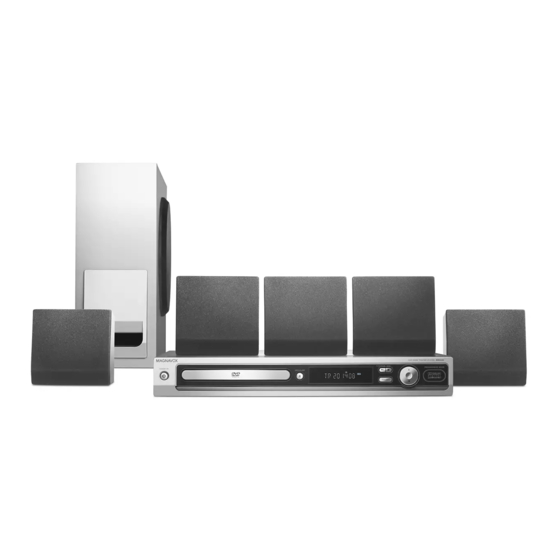
DVD RECEIVER
Service
Service
Service
Service
Service
Service Manual
©
Copyright 2004 Philips Consumer Electronics B.V. Eindhoven, The Netherlands
All rights reserved. No part of this publication may be reproduced, stored in a retrieval system or
transmitted, in any form or by any means, electronic, mechanical, photocopying, or otherwise
without the prior permission of Philips.
Published by HY-ET0512 Service Audio Printed in The Netherlands Subject to modification
Version 1.0
TABLE OF CONTENTS
Location of PC Boards ................................................ 1-2
Versions Variation & Package .................................... 1-2
Specifications .............................................................. 1-3
Measurement Setup ................................................... 1-4
Service Aids ................................................................ 1-5
ESD & Safety Instruction ............................................ 1-6
Lead-free solding Information .................................... 1-7
Repair Instructions ......................................................... 2
Disassembly Instructions & Service positions .............. 3
Block & Wiring Diagram ................................................ 4
Control Board ................................................................. 5
Main Board .................................................................... 6
Tuner Board ................................................................... 7
Power Board .................................................................. 8
DVD loader....................................................................9
Mechanical Exploded View & Parts..............................10
MRD100/
Page
GB
3139 785 32050
78
Advertisement
Table of Contents

Related Manuals for Philips MRD100/78


Summary of Contents for Philips MRD100/78
- Page 1 Mechanical Exploded View & Parts......10 © Copyright 2004 Philips Consumer Electronics B.V. Eindhoven, The Netherlands All rights reserved. No part of this publication may be reproduced, stored in a retrieval system or transmitted, in any form or by any means, electronic, mechanical, photocopying, or otherwise without the prior permission of Philips.
-
Page 2: Location Of Pcb Boards
LOCATION OF PCB BOARDS TUNER MAIN PCB POWER CONTROL... -
Page 3: Specifications
Specifications AMPLIFIER MAIN UNIT Power Supply Rating:120–127V/220–240 V ; Output power: 100 W 50-60 Hz - Front: 15 W / channel - Rear: 15 W / channel Power Consumption: 35 W - Centre: 15 W RMS Dimensions: 360 x 48 x 339 (mm) - Subwoofer: 25 W RMS (w x h x d) -
Page 4: Measurement Setup
MEASUREMENT SETUP Tuner FM Bandpass LF Voltmeter 250Hz-15kHz e.g. PM2534 e.g. 7122 707 48001 RF Generator e.g. PM5326 S/N and distortion meter e.g. Sound Technology ST1700B Use a bandpass filter to eliminate hum (50Hz, 100Hz) and disturbance from the pilottone (19kHz, 38kHz). Tuner AM (MW,LW) Bandpass LF Voltmeter... -
Page 5: Service Aids
SERVICE AIDS Service Tools: Universal Torx driver holder .........4822 395 91019 Torx bit T10 150mm ...........4822 395 50456 Torx driver set T6-T20 .........4822 395 50145 Torx driver T10 extended ........4822 395 50423 Compact Disc: SBC426/426A Test disc 5 + 5A ......4822 397 30096 SBC442 Audio Burn-in test disc 1kHz ....4822 397 30155 SBC429 Audio Signals disc .........4822 397 30184 Dolby Pro-logic Test Disc ........4822 395 10216... -
Page 6: Class 1 Laser Product
WAARSCHUWING WARNING Alle IC’s en vele andere halfgeleiders zijn All ICs and many other semi-conductors are gevoelig voor electrostatische ontladingen susceptible to electrostatic discharges (ESD). (ESD). Careless handling during repair can reduce life Onzorgvuldig behandelen tijdens reparatie kan drastically. de levensduur drastisch doen verminderen. When repairing, make sure that you are Zorg ervoor dat u tijdens reparatie via een connected with the same potential as the mass... - Page 7 You will find this and more technical information • Use only lead-free solder alloy Philips SAC305 with within the “magazine”, chapter “workshop news”. order code 0622 149 00106. If lead-free solder-paste is required, please contact the manufacturer of your For additional questions please contact your local solder-equipment.
- Page 8 In tuner mode, press D11 for more than 5 seconds to change 2) Region Code Change ✤ "1234" is a default password supplied. For MRD100/78 ( LATAM ) : tuner area. After replacement / repair of the MPEG board, the customer <PLAY> <159> <411> <001> <08> <PLAY>...
- Page 9 REPAIR INSTRUCTIONS...
- Page 10 REPAIR INSTRUCTIONS...
- Page 11 DISASSEMBLY INSTRUCTIONS Dismantling of the Main PCB 1) Loosen 5 screw "A" at the back panel as shown in figure 4. Dismantling of the Front Panel Assembly 2) Loosen 4 screw " C " on the top of main board as shown in figure 5.
-
Page 12: Service Positions
SERVICE POSITIONS Dismantling of the DVD Module Service position A 1) Loosen 4 screws "B" to remove the DVD Module as shown in figure 6. Figure 6 Note: In some service positions the components or copper patterns of one board may risk touching its neighbouring pc Dismantling of the Power Board boards or metallic parts. - Page 13 BLOCK DIAGRAM FLASH SDRAM EEPRO M MX 8M IC 4Mx16 24C02 POWER BOARD 74HCU04 Coaxial in DVD MOTOR Drive IC AM5869 EASTWIN LOADER SWITCH POWER M04S SANYO CVBS POWER PCB ASSY230V 100W ES8380C D RF A.B.C.D.E.F MPEG II Decoder DIVX Decoder VIDEO FILTER DOLBY DIGITAL Decoder DOLBY PROG LOGIC Decoder...
- Page 14 WIRING DIAGRAM TUNER BOARD MAIN BOARD POWER BOARD DVD LOADER CONTROL BOARD...
- Page 15 FTD DISPLAY PIN ASSIGNMENT CONTROL BOARD TABLE OF CONTENTS FTD Display Pin Assignment ........... 5-1 Circuit Diagram ..............5-2 PCB Layout Top & Bottom View ........5-3 PIN CONNECTION Pin No. Connection Pin No. Connection ## Note ## 1. Fn: Filament pin 2.
-
Page 16: Circuit Diagram - Control Board
CIRCUIT DIAGRAM - CONTROL BOARD C302 C303 C304 C305 C306 C307 C309 CN101 DP301 C310 R463 MIC OUT ZD301 R301 R302 R305 C311 5.6V C312 C313 RB303 C314 C315 GNDA C316 C319 -27V 7Pin 2.0m m R303 C320 C633 SN301 C634 JK551 C307... -
Page 17: Pcb Layout - Top View
PCB LAYOUT - TOP VIEW C311 DP301 A1 R302 R326 SN301 A4 TA305 C312 R304 RB301A B1 TA301 A5 TA306 D303 JW10 LD301 A8 R305 RB301B B8 TA302 B5 TA308 D305 JW11 R319 A1 R309 RB302 TA303 B6 XL301 D307 R301 A4 R310 RB303... - Page 18 Internal IC diagram - MX29LV800BT WRITE CONTROL PROGRAM/ERASE STATE INPUT HIGH VOLTAGE MACHINE LOGIC RESET# (WSM) STATE REGISTER MAIN BOARD MX29LV800BT/BB ADDRESS FLASH LATCH ARRAY ARRAY A0-A18 SOURCE COMMAND DATA BUFFER Y-PASS GATE DECODER SENSE DATA COMMAND AMPLIFIER DATA LATCH PROGRAM DATA LATCH TABLE OF CONTENTS...
-
Page 19: Circuit Diagram - Top Left
CIRCUIT DIAGRAM - TOP LEFT C121 D6 C147 C166 C194 C209 C226 D11 C244 D4 C261 C277 B6 C291 E5 C313 C337 C409 C453 C468 C483 C826 D104 FB114 E11 C100 C122 A3 C149 C167 C195 C210 C227 E11 C245 D4 C262 C278 B6 C292 A2... -
Page 20: Circuit Diagram - Top Right
CIRCUIT DIAGRAM - TOP RIGHT FB140 IC104 JK801 L118 L802 Q116 R114 R149 R168 R181 R198 R221 R248 R269 R322 R386 R829 C10 R863 ZD110 FB141 IC105 L101 L119 L803 Q117 R115 R169 R182 R223 R249 R302 R323 R387 R559 R830 C10 R922 ZD111... -
Page 21: Circuit Diagram - Bottom Left
CIRCUIT DIAGRAM - BOTTOM LEFT... -
Page 22: Circuit Diagram - Bottom Right
CIRCUIT DIAGRAM - BOTTOM RIGHT... - Page 23 PCB LAYOUT - TOP VIEW...
- Page 24 PCB LAYOUT - BOTTOM VIEW C154 B1 C198 A4 C245 C276 C3 C313 D3 C345 C413 D6 C459 C927 C2 R390 C102 C155 B1 C2 C246 C277 C314 D3 C346 C414 D6 C460 FB123 R391 C103 C156 B1 C204 D2 C247 C278 C316 D4 C347...
- Page 25 VOLTGE IC102A (MX29LV800CBTC) IC111 (SN74LVTH273PWR) Pin NO Pin NO Voltage 5.00 1.70 1.70 1.70 1.73 1.73 1.73 3.00 0.00 0.00 1.85 0.00 0.00 1.73 1.73 1.73 1.73 Voltage 0.00 2.86 1.46 2.42 2.11 1.33 1.20 1.64 0.00 0.00 3.40 5.00 0.00 0.00 0.00...
-
Page 26: Tuner Adjustment Table
TUNER ADJUSTMENT TABLE Waverange Input frequency Input Tuned to Adjust Output Scope/Voltmeter VARICAP ALIGNMENT 108MHz 6.5V 1.2V check 87.5 - 108MHz (50kHz grid) 87.5MHz check 1.0V 0.5V 1602KHz check 7.8V 0.2V T005 1.1V 0.5V 531KHz TUNER BOARD 530-1710kHz (10kHz grid) ( 21L / 21L / 37S ) check 1700KHz... -
Page 27: Circuit Diagram - Tuner Board
CIRCUIT DIAGRAM - TUNER BOARD ANT001 A1 R005 C002 R006 C004 R007 C005 R010 C006 R011 C007 R015 C008 R016 C009 R017 R018 C010 R019 C011 R020 C012 R021 C013 R023 C014 R024 C015 R025 C016 R026 C017 R027 C018 R028 C019 R029... -
Page 28: Pcb Layout - Tuner Board (Top)
PCB LAYOUT - TUNER BOARD (TOP) ANT001 A2 C009 C025 C047 D002 IF001 A1 JMP4 C1 JMP8 C2 Q001 C2 T002 VC001 VD003 C005 C019 C02A CN001 C1 D003 IF002 B2 JMP5 B2 JMP9 B2 Q002 B2 T003 VC001 VD004 C006 C030 CN002 A1... -
Page 29: Pcb Layout - Tuner Board (Bottom)
PCB LAYOUT - TUNER BOARD (BOTTOM) C001 C014 C021 C036 C041 C050 R002 R010 R019 R025 R030 TIP1 TIP14 B1 TIP4 A2 TIP9 B2 C002 C010 C015 C022 C031 C037 C042 C052 R004 R011 R020 R026 R031 TIP10 A1 TIP15 B1 TIP5 A2 C004 C011... - Page 30 Voltage IC 952 Pin NO Voltage 5.00 5.00 3.48 1.40 1.58 3.49 0.00 13.20 0.45 0.43 13.20 13.20 5.00 5.00 5.00 0.00 IC951 Pin NO Voltage 1.36 5.00 1.50 0.00 13.20 5.00 13.00 12.00 IC902 Pin NO Voltage -13.4 128.00 130.00 131.00 132.00...
-
Page 31: Circuit Diagram - Power Board
CIRCUIT DIAGRAM - POWER BOARD BD901 C913 C923 C959 C975 C987 CN951 D4 D954 GT902 B1 L901 Q951 R904 R915 R953 R964 R975 R985 T902 C903 C914 C924 C960 C976 C989 CN952 A3 D955 GT903 C1 L902 Q952 R905 R916 R954 R965 R976... - Page 32 DVD LOADER It is not recommended for component repair on this Module but to replace the major assembly when it becomes defective. Therefore limited service parts list are published in this chapter. TABLE OF CONTENTS Explorer View (DVD Loader)...........9-2...
- Page 33 Explorer View - DVD Loader...
- Page 34 10-1 10-1 EXPLODED DRAWING- MAIN UNIT...
- Page 35 APE106320-0003 9965 000 36120 TUNER PCB ASS’Y APE113960-0063 9965 000 36121 CONTROL PCB ASS’Y APE203060-0002 9965 000 36122 FRONT PANEL MRD100/78 BPF106055-0005 9965 000 36138 FUNTION KNOB ABS SPRAY BPK102105-0001 9965 000 36123 VOL BUTTON D24MM BPK105093-0001 9965 000 36124 RUBBER FOOT DIA14XT3.0MM...