
Related Manuals for Asus AAEON GENESYSM-TGU6


Summary of Contents for Asus AAEON GENESYSM-TGU6
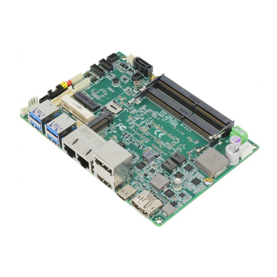
- Page 1 GENESYSM-TGU6 GENESYSM Compact Embedded System User’s Manual 1 Last Updated: September 19, 2022...
- Page 2 Copyright Notice This document is copyrighted, 2022. All rights are reserved. The original manufacturer reserves the right to make improvements to the products described in this manual at any time without notice. No part of this manual may be reproduced, copied, translated, or transmitted in any form or by any means without the prior written permission of the original manufacturer.
- Page 3 Acknowledgements All other products’ name or trademarks are properties of their respective owners. Microsoft Windows is a registered trademark of Microsoft Corp. ⚫ Intel® and Celeron® are registered trademarks of Intel Corporation ⚫ Intel Core™ are trademarks of Intel Corporation ⚫...
- Page 4 Packing List Before setting up your product, please make sure the following items have been shipped: Item Quantity GENESYSM-TGU6 If any of these items are missing or damaged, please contact your distributor or sales representative immediately. Preface...
- Page 5 About this Document This User’s Manual contains all the essential information, such as detailed descriptions and explanations on the product’s hardware and software features (if any), its specifications, dimensions, jumper/connector settings/definitions, and driver installation instructions (if any), to facilitate users in setting up their product. Users may refer to the product page at AAEON.com for the latest version of this document.
- Page 6 Safety Precautions Please read the following safety instructions carefully. It is advised that you keep this manual for future references All cautions and warnings on the device should be noted. Make sure the power source matches the power rating of the device. Position the power cord so that people cannot step on it.
- Page 7 If any of the following situations arises, please the contact our service personnel: Damaged power cord or plug Liquid intrusion to the device iii. Exposure to moisture Device is not working as expected or in a manner as described in this manual The device is dropped or damaged Any obvious signs of damage displayed on the device...
- Page 8 FCC Statement This device complies with Part 15 FCC Rules. Operation is subject to the following two conditions: (1) this device may not cause harmful interference, and (2) this device must accept any interference received including interference that may cause undesired operation.
- Page 9 China RoHS Requirements (CN) 产品中有毒有害物质或元素名称及含量 AAEON Main Board/ Daughter Board/ Backplane 有毒有害物质或元素 部件名称 铅 汞 镉 六价铬 多溴联苯 多溴二苯醚 (Pb) (Hg) (Cd) (Cr(VI)) (PBB) (PBDE) 印刷电路板 ○ ○ ○ ○ ○ ○ 及其电子组件 外部信号 ○ ○ ○ ○ ○ ○ 连接器及线材...
- Page 10 China RoHS Requirement (EN) Poisonous or Hazardous Substances or Elements in Products AAEON Main Board/ Daughter Board/ Backplane Poisonous or Hazardous Substances or Elements Hexavalent Polybrominated Polybrominated Component Lead Mercury Cadmium Chromium Biphenyls Diphenyl Ethers (Pb) (Hg) (Cd) (Cr(VI)) (PBB) (PBDE) PCB &...
-
Page 11: Table Of Contents
Table of Contents Chapter 1 - Product Specifications..................1 Specifications ......................2 Block Diagram ......................6 Chapter 2 – Hardware Information ..................7 Dimensions ....................... 8 Jumpers and Connectors ..................10 List of Jumpers ......................12 2.3.1 Front Panel Connector (JP1) ................ 12 2.3.2 Auto Power Button Enable/Disable Selection (JP3) ....... - Page 12 2.4.15 USB 3.2 Gen 2 Ports 1 & 2 Dual Connector (CN26) ......26 2.4.16 LAN (RJ-45) Dual Port i225/i226 and i219 (CN27) ........ 27 2.4.17 DP Connector (CN28) ................. 27 2.4.18 DP + HDMI Connector (CN29) ..............29 2.4.19 USB Type C (CN30) ..................
- Page 13 3.4.4.1 Firmware Update Configuration ............. 61 3.4.5 Power Management ..................62 3.4.6 AAEON BIOS Robot ..................63 3.4.6.1 Device Detecting Configuration ............ 65 3.4.7 TSN GBE Configuration ................77 Setup Submenu: System I/O ................78 3.5.1 PCI Express Configuration ................79 3.5.2 Storage Configuration ................
- Page 14 Appendix B – Mating Connectors and Cables ..............107 Mating Connectors and Cables ................ 108 Preface...
-
Page 15: Chapter 1 - Product Specifications
Chapter 1 Chapter 1 - Product Specifications... -
Page 16: Specifications
Specifications System Form Factor 3.5" SubCompact Board System Intel® 11th Generation Core™/Celeron CPU i7-1185G7E (4C/8T, 1.80GHz, up to 4.40GHz, TDP-up 28W) i5-1145G7E (4C/8T, 1.50GHz, up to 4.10GHz, TDP-up 28W) i3-1115G4E (2C/4T, 2.20GHz, up to 3.90GHz, TDP-up 28W) Celeron® 6305E (2C/2T, 1.80GHz, TDP 15W) Chipset Integrated with Intel®... - Page 17 Power Power Requirement +9-36V (Optional +12V) Power Supply Type Connector DC Jack Connector Power Consumption Intel® i7-1185G7E, DDR4 3200MHz 32GB x 2, 4.96A@ +12V (typical) Intel® i7-1185G7E, DDR4 3200MHz 32GB x 2, 7.32A@ +12V (max) Display Controller Intel® Iris® X Graphics Intel®...
- Page 18 External I/O Ethernet Intel® i219, 10/100/1000Base, RJ-45 x 1 Intel® i225/i226, 10/100/2500Base, RJ-45 x 1 USB 3.2 Gen 2 x 4 USB 3.2 Gen 2 Type C x 1 (PD 5V/3A) USB 2.0 x 2 Serial Port COM1 (RS232/422/485) COM2 (RS232/422/485, supports 5V/12V/RI) Video HDMI 2.0b x 1 DP 1.4 x 2...
- Page 19 Expansion Mini PCI-E/mSATA Full-Sized mSATA/mPCIe x 1 (default: mSATA, select with BIOS) M-Key 2280 x 1 (PCIex4) E-Key 2230 x 1 (PCIe, USB 2.0) Others Environment Operating Temperature 32°F ~ 122°F (0°C ~ 50°C) Storage Temperature -40°F ~ 185°F (-40°C ~ 85°C) Operating Humidity 0% ~ 90% relative humidity, non-condensing MTBF (HOURS)
-
Page 20: Block Diagram
Block Diagram Chapter 1 – Product Specifications... -
Page 21: Chapter 2 - Hardware Information
Chapter 2 Chapter 2 – Hardware Information... -
Page 22: Dimensions
Dimensions System Chapter 2 – Hardware Information... - Page 23 Board Chapter 2 – Hardware Information...
-
Page 24: Jumpers And Connectors
Jumpers and Connectors Component Side: Front I/O: Chapter 2 – Hardware Information... - Page 25 Solder Side: Chapter 2 – Hardware Information...
-
Page 26: List Of Jumpers
List of Jumpers Please refer to the table below for all of the board’s jumpers that you can configure for your application Label Function Front Panel Connector Auto Power Button Enable/ Disable Selection COM2 Pin 8 Function Selection Clear CMOS Jumper 2.3.1 Front Panel Connector (JP1) Function... -
Page 27: Auto Power Button Enable/Disable Selection (Jp3)
2.3.2 Auto Power Button Enable/Disable Selection (JP3) 1 2 3 Disable/ Enable/ ATX Power Mode (Default) AT Power Mode 2.3.3 COM2 Pin8 Function Selection (JP4) +12V Ring (Default) 2.3.4 Clear CMOS Jumper (JP7) 1 2 3 Normal (Default) Clear CMOS Chapter 2 –... -
Page 28: List Of Connectors
List of Connectors Please refer to the table below for all of the board’s connectors that you can configure for your application Label Function +5V Output for SATA HDD SATA Port External Power Input Audio I/O Port External +5VSB Input DDR4 SO-DIMM Slot CN10 Mini Card Slot (Full-Size) -
Page 29: Output For Sata Hdd (Cn1)
Label Function CN33 M.2 M-Key 2280 CN35 USB3.2 Gen 2 Port 3, Port 4, Dual Port Connector CN36 i219 LED Connector CN37 i225/i226 LED Connector 2.4.1 +5V Output for SATA HDD (CN1) Pin Name Signal Type Signal Level +5V at 1A Note: Max current for Pin 1 is 1 Amp. -
Page 30: Sata Port (Cn2)
2.4.2 SATA Port (CN2) Pin 1 Pin 7 Pin Name Signal Type Signal Level SATA_TX+ DIFF SATA_TX- DIFF SATA_RX- DIFF SATA_RX+ DIFF 2.4.3 External Power Input (CN3) Pin Name Signal Type Signal Level +12V +9~+36V (or +12V) at 8A Note: There are two types of power input, 9~36V or 12V (by BOM option). Chapter 2 –... -
Page 31: Audio I/O Port (Cn5)
2.4.4 Audio I/O Port (CN5) Pin Name Signal Type LOUT_R MIC_R LOUT_L MIC_L JD_LOUT JD_MIC AUD_GND AUD_GND JD_LIN LIN_R +VDD_AUD LIN_L Chapter 2 – Hardware Information... -
Page 32: External +5Vsb Input (Cn6)
2.4.5 External +5VSB Input (CN6) Pin Name Signal Type Signal Level PS_ON# +5VSB +5V at 2A 2.4.6 DDR SO-DIMM Slot (CN7) Standard Specifications. Chapter 2 – Hardware Information... -
Page 33: Mini Card Slot (Full-Size) (Cn10)
2.4.7 Mini Card Slot (Full-Size) (CN10) Pin Name Signal Type Signal Level PCIE_WAKE# +3.3VSB +3.3V +1.5V +1.5V PCIE_CLK_REQ# UIM_PWR UIM_DATA PCIE_REF_CLK- DIFF UIM_CLK PCIE_REF_CLK+ DIFF UIM_RST UIM_VPP W_DISABLE# +3.3V PCIE_RST# +3.3V PCIE_RX- DIFF +3.3VSB +3.3V Chapter 2 – Hardware Information... - Page 34 Pin Name Signal Type Signal Level PCIE_RX+ DIFF +1.5V +1.5V SMB_CLK +3.3V PCIE_TX- DIFF SMB_DATA +3.3V PCIE_TX+ DIFF USB_D- DIFF USB_D+ DIFF +3.3VSB +3.3V +3.3VSB +3.3V +1.5V +1.5V Chapter 2 – Hardware Information...
-
Page 35: Ddr So-Dimm Slot (Cn11)
Pin Name Signal Type Signal Level +3.3VSB +3.3V 2.4.8 DDR SO-DIMM Slot (CN11) Standard Specifications. 2.4.9 M.2 E-Key 2230 (CN12) Standard Specifications. 2.4.10 COM Port 1, Port 2 Dual Header (CN13) RS-232 Pin Name Signal Type Signal Level ±5V ±5V Chapter 2 –... - Page 36 Pin Name Signal Type Signal Level ±5V RI/+5V/+12V Note: RI/+5V/+12V for COM2 only. RS-485 Pin Name Signal Type Signal Level RS485_D- ±5V RS485_D+ ±5V RS-422 Pin Name Signal Type Signal Level RS422_TX- RS422_TX+ ±5V RS422_RX+ RS422_RX- Chapter 2 – Hardware Information...
-
Page 37: Espi Debug Port (Cn16)
Pin Name Signal Type Signal Level Note 1: COM2 RS-232/422/485 can be set by BIOS setting. Default is RS-232. Note 2: Pin 8 function can be set by JP4 (See Ch 2.3.4). 2.4.11 eSPI Debug Port (CN16) Pin Name Signal Type Signal Level LAD0 +3.3V... -
Page 38: Nano Sim Card Socket (Cn19)
Pin Name Signal Type Signal Level LCLK SMB_DATA/I2C_SDA SMB_CLK/I2C_CLK SMB_ALERT/SERIRQ +3.3V 2.4.12 Nano SIM Card Socket (CN19) Pin Name Signal Type Signal Level UIM_PWR UIM_RST UIM_CLK UIM_VPP UIM_DATA Chapter 2 – Hardware Information... -
Page 39: Usb 2.0 Port 5, Port 6 Dual Header (Cn21)
2.4.13 USB 2.0 Port 5, Port 6 Dual Header (CN21) USB Port 5 USB Port 6 Pin Name Pin Name +5VSB (0.5A) +5VSB (0.5A) USB5_D- USB6_D- USB5_D+ USB6_D+ 2.4.14 CPU Fan (CN23) Pin Name Signal Type Signal Level FAN_POWER +12V at 1A FAN_TAC FAN_CTL Chapter 2 –... -
Page 40: Usb 3.2 Gen 2 Ports 1 & 2 Dual Connector (Cn26)
2.4.15 USB 3.2 Gen 2 Ports 1 & 2 Dual Connector (CN26) Pin Name Signal Type Signal Level +5VSB +5V at 0.9A USB0_D- DIFF USB0_D+ DIFF USB0_SSRX− DIFF USB0_SSRX+ DIFF USB0_SSTX− DIFF USB0_SSTX+ DIFF +5VSB +5V at 0.9A USB1_D- DIFF USB1_D+ DIFF USB1_SSRX−... -
Page 41: Lan (Rj-45) Dual Port I225/I226 And I219 (Cn27)
2.4.16 LAN (RJ-45) Dual Port i225/i226 and i219 (CN27) i225/i226 i219 Pin Name Pin Name LAN2_MDI0_P LAN1_MDI0_P LAN2_MDI0_N LAN1_MDI0_N LAN2_MDI1_P LAN1_MDI1_P LAN2_MDI1_N LAN1_MDI1_N LAN2_MDI2_P LAN1_MDI2_P LAN2_MDI2_N LAN1_MDI2_N LAN2_MDI3_P LAN1_MDI3_P 1P10 LAN2_MDI3_N 2P10 LAN1_MDI3_N 2.4.17 DP Connector (CN28) Pin Name Signal Type Signal Level DP1_TX0_DP DIFF... - Page 42 Pin Name Signal Type Signal Level DP1_TX0_DN DIFF DP1_TX1_DP DIFF DP1_TX1_DN DIFF DP1_TX2_DP DIFF DP1_TX2_DN DIFF DP1_TX3_DP DIFF DP1_TX3_DN DIFF DP1_AUX_DP DP1_AUX_DN DP1_HPD +V3P3S +3.3V Chapter 2 – Hardware Information...
-
Page 43: Dp + Hdmi Connector (Cn29)
2.4.18 DP + HDMI Connector (CN29) Pin Name Signal Type Signal Level DP Port DP2_TX0_DP DIFF DP2_TX0_DN DIFF DP2_TX1_DP DIFF DP2_TX1_DN DIFF DP2_TX2_DP DIFF DP2_TX2_DN DIFF DP2_TX3_DP DIFF DP2_TX3_DN DIFF DP2_AUX_DP Chapter 2 – Hardware Information... - Page 44 Pin Name Signal Type Signal Level DP2_AUX_DN DP2_HPD +V3P3S +3.3V HDMI Port HDMI_TX2+ DIFF HDMI_TX2- DIFF HDMI_TX1+ DIFF HDMI_TX1- DIFF HDMI_TX0+ DIFF HDMI_TX0- DIFF HDMI_CLK+ DIFF HDMI_CLK- DIFF DDC_CLK DDC_DATA HDMI_HPD Chapter 2 – Hardware Information...
-
Page 45: Usb Type C (Cn30)
2.4.19 USB Type C (CN30) Pin Name Signal Type Signal Level TCP2_TX0_DP DIFF TCP2_TX0_DN DIFF +5VSB CON_CC1 USB2_8_DP DIFF USB2_8_DN DIFF CONN_TYPEC1_SBU1 DIFF +5VSB TCP2_TXRX1_DN DIFF TCP2_TXRX1_DP DIFF TCP2_TX1_DP DIFF TCP2_TX1_DN DIFF +5VSB CONN_TYPEC1_CC2 Chapter 2 – Hardware Information... -
Page 46: Battery Connector (Cn31)
Pin Name Signal Type Signal Level USB2_8_DP DIFF USB2_8_DN DIFF CONN_TYPEC1_SBU2 DIFF +5VSB TCP2_TXRX0_DN DIFF TCP2_TXRX0_DP DIFF Note: Type C Power current support => 5V/3A 2.4.20 Battery Connector (CN31) Pin Name Signal Type Signal Level +3.3V 3.3V Chapter 2 – Hardware Information... -
Page 47: Spi Bios Debug Port (Cn32)
2.4.21 SPI BIOS Debug Port (CN32) Pin Name Signal Type Signal Level SPI_MISO SPI_CLK +3.3VSB +3.3V SPI_MOSI SPI_CS Chapter 2 – Hardware Information... -
Page 48: M-Key 2280 Slot (Cn33)
2.4.22 M.2 M-Key 2280 Slot (CN33) Standard specifications. 2.4.23 USB3.2 Gen 2 Ports 3 & 4 Dual Connector (CN35) Pin Name Signal Type Signal Level +5VSB +5V at 0.9A USB2_D- DIFF USB2_D+ DIFF USB2_SSRX− DIFF USB2_SSRX+ DIFF USB2_SSTX− DIFF USB2_SSTX+ DIFF +5VSB +5V at 0.9A... -
Page 49: I219 Led Connector (Cn36)
Pin Name Signal Type Signal Level USB3_SSTX− DIFF USB3_SSTX+ DIFF 2.4.24 i219 LED Connector (CN36) Pin Name Signal Type Signal Level LINK_ACT# +V3P3A +3.3V LAN_1000# LAN_100# LAN_100# LAN_1000# Chapter 2 – Hardware Information... -
Page 50: I225/I226 Led Connector (Cn37)
2.4.25 i225/i226 LED Connector (CN37) Pin Name Signal Type Signal Level LINK_ACT# +V3P3A +3.3V LAN_2500# LAN_1000# LAN_1000# LAN_2500# Chapter 2 – Hardware Information... -
Page 51: Hardware Installation
Hardware Installation This section details the steps needed to install various hardware components for the GENESYSM-TGU6. It is recommended that you read through each step before beginning installation and to make sure you have all necessary tools and components. 2.5.1 Accessing the Bottom Panel For this process you will need a Phillips head screwdriver. - Page 52 Chapter 2 – Hardware Information...
-
Page 53: Ram Module Installation
2.5.2 RAM Module Installation Before you begin, make sure you have the RAM module(s) you wish to install ready. Memory Slot Memory Slot CN11 Step 1: Insert the RAM module in the DDR SO-DIMM Slot (CN7) at about 45° angle, then gently press down until it is secured by the tabs. -
Page 54: 2.5" Sata Drive Installation
2.5.3 2.5” SATA Drive Installation Before beginning, make sure you have the following prepared: SATA Drive x 1 • Black Screws x 4 (to mount 2.5” drive) • SATA Cable x 1 • SATA Power Cable x 1 • Phillips head screwdriver •... - Page 55 Step 2: Line up the mounting holes on the SATA drive with the four mounting points on the bottom panel. Note the orientation of the cables. Step 3: Secure the drive with four black mounting screws. Chapter 2 – Hardware Information...
- Page 56 Step 4: Insert the SATA Cable into CN2 and SATA Power Cable into CN1. If you are finished with hardware installation, replace the back panel and secure with two black screws. Otherwise, continue to the next section for COM Port installation. Chapter 2 –...
-
Page 57: Com Port Installation
2.5.4 COM Port Installation Before beginning installation, please ensure you have the following: COM Port Connector with cables x 1 • Jack standoffs x 4 (two included with each COM Port Connector) • Phillips head screwdriver • Note: This procedure will require opening both the top and bottom panels. Take care if you have already installed the 2.5”... - Page 58 Step 1: Hand loosen the spring mounted case screws securing the top panel to the rear panel of the system. The top panel will swing open towards the front panel. Step 2: Remove the COM Port knockouts by pushing with a finger or tool. Chapter 2 –...
- Page 59 Step 3: Fasten the COM Port Connectors to the appropriate knockouts using the four jack standoffs. Then, feed the cables around the side of the heatsink and board as shown. Chapter 2 – Hardware Information...
- Page 60 Step 4: Access the bottom side of the board. Carefully route the cables around the board and connect to the appropriate board connector. It may help to do each cable one at a time to ensure the ports are connected correctly. COM Port Connector Step 5: Reattach the bottom panel and secure with two black screws.
-
Page 61: Wallmount Assembly
2.5.5 Wallmount Assembly Before beginning, ensure all panels on the system are secured. Then make sure you have to following components ready: Wallmount brackets x 2 • Black screws x 4 (two for each bracket) • Phillips head screwdriver • Line up the brackets with the four open holes on the bottom panel of the system as shown, then secure brackets with the four screws. -
Page 62: Vesa Mount Installation
2.5.6 VESA Mount Installation Before beginning, ensure all panels on the system are secured. Then make sure you have to following components ready: Silver screws with washers x 4 (rounded head) • VESA Mount screws x 2 (head is flat) •... - Page 63 The system can now be attached to the VESA bracket. Mount the bracket to a surface or the back of a display/monitor with VESA attachment points. Use the four silver screws with washers to secure the bracket to the back of the monitor with the arrow pointing up.
-
Page 64: Chapter 3 - Ami Bios Setup
Chapter 3 Chapter 3 - AMI BIOS Setup... -
Page 65: System Test And Initialization
System Test and Initialization The GENESYSM-TGU6 uses certain routines to perform testing and initialization during the boot up sequence. If an error, fatal or non-fatal, is encountered, the module will output a few short beeps or display an error message. The module can usually continue the boot up sequence with non-fatal errors. -
Page 66: Ami Bios Setup
AMI BIOS Setup The AMI BIOS ROM has a pre-installed Setup program that allows users to modify basic system configurations, which is stored in the battery-backed CMOS RAM and BIOS NVRAM so that the information is retained when the power is turned off. To enter BIOS Setup, press <Del>... -
Page 67: Setup Submenu: Main
Setup Submenu: Main Chapter 3 – AMI BIOS Setup... -
Page 68: Setup Submenu: Advanced
Setup Submenu: Advanced Options Summary In-Band ECC Support Disabled Enabled Optimal Default; Failsafe Default Enable/Disabled In-Band ECC Support In-Band ECC Error Enabled Injection Disabled Optimal Default, Failsafe Default By enabling this Error Injection feature, the user acknowledges the security risks. Enabling Error Injection allows attackers who have access to the Host Operating System to inject IBECC errors that can cause unintended memory corruption and enable the leak of security data in the BIOS stolen memory regions. -
Page 69: Cpu Configuration
Options Summary IBECC Protect Region 0-7 Disabled Optimal Default, Failsafe Default Enabled Enable/Disabled In-Band ECC for Region 0-7. Note: In-Band ECC Support availability depends on CPU. 3.4.1 CPU Configuration Options Summary Intel (VMX) Virtualization Disabled Technology Enabled Optimal Default, Failsafe Default When enabled, a VMM can utilize the additional hardware capabilities provided by Vanderpool Technology. -
Page 70: Memory Configuration
Options Summary Turbo Mode Disabled Enabled Optimal Default, Failsafe Default Enable/Disable processor Turbo Mode (requires EMTTM enabled too). AUTO means enabled. 3.4.2 Memory Configuration Chapter 3 – AMI BIOS Setup... -
Page 71: Hardware Monitor
3.4.3 Hardware Monitor Options Summary Smart Fan Disabled Enabled Optimal Default, Failsafe Default Enable or Disable Smart Fan. Chapter 3 – AMI BIOS Setup... -
Page 72: Smart Fan Mode Configuration
3.4.3.1 Smart Fan Mode Configuration Auto Duty Cycle Mode Options Summary FAN1 Output Mode Output PWM mode (push pull) Linear Fan Application Output PWM mode Optimal Default, Failsafe Default (open drain) Output PWM mode (push pull) to control 4-wire fans.\nLinear fan application circuit to control 3-wire fan speed by fan’s power terminal.\nOutput PWM mode (open drain) to control Intel 4-wire fans. - Page 73 Options Summary Duty Cycle Auto fan speed control. Fan speed will follow different temperature by different duty cycle 1-100. Temperature Manual Duty Mode Options Summary Manual Duty Mode Optimal Default, Failsafe Default Manual mode fan control, user can write expected duty cycle (PWM fan type) 1-100. Chapter 3 –...
-
Page 74: Pch-Fw Configuration
3.4.4 PCH-FW Configuration Chapter 3 – AMI BIOS Setup... -
Page 75: Firmware Update Configuration
3.4.4.1 Firmware Update Configuration Options Summary Me FW Image Re-Flash Disabled Optimal Default, Failsafe Default Enabled Enable/Disable Me FW Image Re-Flash function. FW Update Disabled Enabled Optimal Default, Failsafe Default Enable/Disable ME FW Update function. Chapter 3 – AMI BIOS Setup... -
Page 76: Power Management
3.4.5 Power Management Options Summary Power Mode ATX Type Optimal Default, Failsafe Default AT Type Select system power mode. Restore AC Power Loss Last State Optimal Default, Failsafe Default Always On Always Off IO Restore AC power Loss. RTC wake system from S5 Disable Optimal Default, Failsafe Default Fixed Time... -
Page 77: Aaeon Bios Robot
3.4.6 AAEON BIOS Robot Options Summary Sends watch dog before Disabled Optimal Default, Failsafe Default BIOS POST Enabled Enabled - Robot set Watch Dog Time (WDT) right after power on, before BIOS start POST process. Robot will clear WDT on completion of POST. WDT will reset system automatically if it is not cleared before its timer counts down to zero. - Page 78 Options Summary OS Timer (minute) Optimal Default, Failsafe Default Timer count set to Watch Dog Timer for OS loading. Delayed POST (PEI phase) Disabled Optimal Default, Failsafe Default Enabled Enabled - Robot holds BIOS from starting POST, right after power on. This allows BIOS POST to start with stable power or start after system is physically warmed-up.
-
Page 79: Device Detecting Configuration
3.4.6.1 Device Detecting Configuration Action: Rest System Options Summary Action Reset System Optimal Default, Failsafe Default Hold System Select action that robot should do. Soft or hard reset Soft Optimal Default, Failsafe Default Hard Select reset type robot should send on each boot. Retry-Count Optimal Default, Failsafe Default Fill retry counter here. - Page 80 Action: Hold System Options Summary Action Reset System Optimal Default, Failsafe Default Hold System Select action that robot should do. Holding time out Optimal Default, Failsafe Default (second) Fill hold time out here. Robot will hold system no longer then time-out value, and then let system continue its POST.
- Page 81 3.4.6.1.1 Device # Detecting Configuration Interface: Disabled Options Summary Interface Disabled Optimal Default, Failsafe Default SMBUS Legacy I/O Super I/O MMIO Select interface robot should use to communicate with device. Chapter 3 – AMI BIOS Setup...
- Page 82 Interface: PCI Options Summary Optimal Default, Failsafe Default Fill BUS number to a PCI device, in hexadecimal. Range: 0 – FF. Device Optimal Default, Failsafe Default Fill DEVICE number to a PCI device, in hexadecimal. Range: 0 – FF. Function Optimal Default, Failsafe Default Fill FUNCTION number to a PCI device, in hexadecimal.
- Page 83 Options Summary Register data is bitwise equal to Optimal Default, Failsafe Default bytewise equal to bytewise lesser than bytewise larger than Select how robot should compare data read from register, to a value configured below. Register offset Optimal Default, Failsafe Default Fill register offset (or index) for robot to read, in hexadecimal.
- Page 84 Interface: DIO Options Summary Device Is not Optimal Default, Failsafe Default Select that robot should or should not do action if condition met. DIO pin number DIO1 Optimal Default, Failsafe Default DIO* Fill DIO pin number. 0 - DIO0, 1 - DIO1, and so on. For COM express product: 0-3 - GPI0-3, 4-7 - GPO0-3.
- Page 85 Interface: SMBUS Options Summary SMBUS Slave Address Optimal Default, Failsafe Default Fill slave address to a SMBUS device, in hexadecimal. Range: 0 – FF. Device Is not Optimal Default, Failsafe Default Select that robot should or should not do action if condition met. In condition Present Optimal Default, Failsafe Default...
- Page 86 Options Summary Register offset Optimal Default, Failsafe Default Fill register offset (or index) for robot to read, in hexadecimal. Range: 0 – FF. Bit offset Optimal Default, Failsafe Default Fill bit offset for register, for robot to compare with bit value. Bit value Optimal Default, Failsafe Default High...
- Page 87 Options Summary In condition Present Optimal Default, Failsafe Default Specified register data Select the condition that robot should check for device. Present - device is detected. According to register - Robot read register according to configuration. Note: Device will be considered 'Present' by Robot, when data read from device is not 0xFF.
- Page 88 Interface: Super I/O Options Summary Super I/O LDN Optimal Default, Failsafe Default Fill LDN number to a Super I/O device. Range: 0~FF Device Is not Optimal Default, Failsafe Default Select that robot should or should not do action if condition met. In condition Present Optimal Default, Failsafe Default...
- Page 89 Options Summary Register offset Optimal Default, Failsafe Default Fill register offset (or index) for robot to read, in hexadecimal. Range: 0 – FF. Bit offset Optimal Default, Failsafe Default Fill bit offset for register, for robot to compare with bit value. Bit value Optimal Default, Failsafe Default High...
- Page 90 Options Summary In condition Present Optimal Default, Failsafe Default Specified register data Select the condition that robot should check for device. Present - device is detected. According to register - Robot read register according to configuration. Note: Device will be considered 'Present' by Robot, when data read from device is not 0xFF.
-
Page 91: Tsn Gbe Configuration
3.4.7 TSN GBE Configuration Options Summary PCH TSN LAN Enabled Optimal Default, Failsafe Default Controller Disabled Enable/Disable TSN LAN. Enable Timed TSN Disabled Optimal Default, Failsafe Default Enabled Enable/Disable TSN PCS. When enabled, TSN PCS device will appear in ACPI table PCH TSN Multi-Vc Disabled Optimal Default, Failsafe Default... -
Page 92: Setup Submenu: System I/O
Setup Submenu: System I/O Chapter 3 – AMI BIOS Setup... -
Page 93: Pci Express Configuration
3.5.1 PCI Express Configuration Options Summary PCI Express Root Port 5 Enabled Optimal Default, Failsafe Default (CN12) / Port11 Disabled Control the PCI Express Root Port. PCIe Speed Auto Optimal Default, Failsafe Default Gen1 Gen2 Gen3 Control the PCI Express Speed. Chapter 3 –... -
Page 94: Storage Configuration
3.5.2 Storage Configuration Options Summary SATA Controller(s) Disabled Enabled Optimal Default, Failsafe Default Enable/Disable SATA Device. Port 0 / 1 Disabled Enabled Optimal Default, Failsafe Default Enable or Disable SATA Port. Hot Plug Disabled Optimal Default, Failsafe Default Enabled Designates this port as Hot Pluggable. Chapter 3 –... -
Page 95: Nvme Configuration
3.5.2.1 NVMe Configuration Chapter 3 – AMI BIOS Setup... -
Page 96: Hd Audio Subsystem Configuration Settings
3.5.3 HD Audio Subsystem Configuration Settings Options Summary HD Audio Disabled Enabled Optimal Default, Failsafe Default Control Detection of the HD-Audio device. Disabled = HDA will be unconditionally disabled. Enabled = HDA will be unconditionally enabled. Chapter 3 – AMI BIOS Setup... -
Page 97: Legacy Logical Devices Configuration
3.5.4 Legacy Logical Devices Configuration Chapter 3 – AMI BIOS Setup... -
Page 98: Serial Port 1 Configuration
3.5.4.1 Serial Port 1 Configuration Options Summary Use This Device Disable Enable Optimal Default, Failsafe Default Enable or Disable this Logical Device. Possible: Use Automatic Settings Optimal Default, Failsafe Default IO=3F8h; IRQ=4 IO=2F8h; IRQ=3 Allows user to change Device's Resource settings. New settings will be reflected on This Setup Page after System restarts. -
Page 99: Serial Port 2 Configuration
3.5.4.2 Serial Port 2 Configuration Options Summary Use This Device Disable Enable Optimal Default, Failsafe Default Enable or Disable this Logical Device. Possible: Use Automatic Settings Optimal Default, Failsafe Default IO=2F8h; IRQ=3 IO=3F8h; IRQ=4 Allows user to change Device's Resource settings. New settings will be reflected on This Setup Page after System restarts. -
Page 100: Serial Port Console Redirection
3.5.5 Serial Port Console Redirection Options Summary Console Redirection Disabled Optimal Default, Failsafe Default Enabled Console Redirection Enable or Disable. Console Redirection EMS Disabled Optimal Default, Failsafe Default Enabled Console Redirection Enable or Disable. Chapter 3 – AMI BIOS Setup... -
Page 101: Console Redirection Settings
3.5.5.1 Console Redirection Settings Options Summary Terminal Type VT100 VT100+ VT-UTF8 ANSI Optimal Default, Failsafe Default Emulation: ANSI: Extended ASCII char set. VT100: ASCII char set. VT100+: Extends VT100 to support color, function keys, etc. VT-UTF8: Uses UTF8 encoding to map Unicode chars onto 1 or more bytes. - Page 102 Options Summary Data Bits. Parity None Optimal Default, Failsafe Default Even Mark Space A parity bit can be sent with the data bits to detect some transmission errors. Even: parity bit is 0 if the num of 1's in the data bits is even. Odd: parity bit is 0 if num of 1's in the data bits is odd.
-
Page 103: Pch-Io Configuration
3.5.6 PCH-IO Configuration Options Summary MiniCard Slot Function SATA Optimal Default, Failsafe Default PCIe Select function enabled for Full size MiniCard Slot (CN10). Chapter 3 – AMI BIOS Setup... -
Page 104: Setup Submenu: Security
Setup Submenu: Security Change User/Administrator Password You can set an Administrator Password or User Password. An Administrator Password must be set before you can set a User Password. The password will be required during boot up, or when the user enters the Setup utility. A User Password does not provide access to many of the features in the Setup utility. -
Page 105: Trusted Computing
3.6.1 Trusted Computing Options Summary Security Device Support Disable Enable Optimal Default, Failsafe Default Enables or Disables BIOS support for security device. O.S. will not show Security Device. TCG EFI protocol and INT1A interface will not be available. SHA-1 PCR Bank Disable Enable Optimal Default, Failsafe Default... - Page 106 Options Summary Platform Hierarchy Disabled Enabled Optimal Default, Failsafe Default Enable or disable Platform Hierarchy. Storage Hierarchy Disabled Enabled Optimal Default, Failsafe Default Enable or Disable Storage Hierarchy. Endorsement Hierarchy Disabled Enabled Optimal Default, Failsafe Default Enable or Disable Endorsement Hierarchy. TPM2.0 UEFI Spec Version TCG_1_2 TCG_2...
-
Page 107: Secure Boot
3.6.2 Secure Boot Options Summary Secure Boot Disabled Optimal Default, Failsafe Default Enabled Secure Boot feature is Active if Secure Boot is Enabled, Platform Key (PK) is enrolled and the System is in User mode. The mode change requires platform reset. Secure Boot Mode Custom Optimal Default, Failsafe Default... -
Page 108: Setup Submenu: Boot
Setup Submenu: Boot Options Summary Quiet Boot Disabled Enabled Optimal Default, Failsafe Default Enables or disables showing boot logo. Network Stack Disabled Optimal Default, Failsafe Default Enabled Enable/Disable UEFI Network Stack. Chapter 3 – AMI BIOS Setup... -
Page 109: Bbs Priorities
3.7.1 BBS Priorities Chapter 3 – AMI BIOS Setup... -
Page 110: Setup Submenu: Save & Exit
Setup Submenu: Save & Exit Chapter 3 – AMI BIOS Setup... -
Page 111: Chapter 4 - Driver Installation
Chapter 4 Chapter 4 – Driver Installation... -
Page 112: Driver Download/Installation
Driver Download/Installation Drivers for the GENESYSM-TGU6 can be downloaded from the product page on the AAEON website by following this link: https://www.aaeon.com/en/p/3-and-half-inch-sbc-genesysm-tgu6 Download the driver(s) you need and follow the steps below to install them. Audio Driver (Windows 10) Open the folder where you unzipped the Audio Drivers Run the Setup.exe in the folder Follow the instructions Drivers will be installed automatically... - Page 113 LAN Drivers (Windows 10) Open the folder where you unzipped the LAN Drivers Read the ReadMe.txt file before proceeding. Caution: Be sure to install the driver package before installing the Intel® PROSet package. Open the Wired_driver_26.3_x64 folder Run the Wired_driver_26.3_x64.exe file in the folder Follow the instructions, drivers will be installed automatically.
- Page 114 Touch Drivers (Windows 10) Open the folder where you unzipped the Peripheral Drivers Run the Setup.exe file in the folder Follow the instructions Drivers will be installed automatically Peripheral Driver (Linux) Open the folder where you unzipped the Peripheral Drivers Follow the instructions contained within the user guides Touch Drivers (Linux) Touch Drivers can be installed via terminal, or through the graphical UI if...
-
Page 115: Appendix A - I/O Information
Appendix A Appendix A - I/O Information... -
Page 116: I/O Address Map
I/O Address Map Appendix A – I/O Information... -
Page 117: A.2 Memory Address Map
A.2 Memory Address Map Appendix A – I/O Information... - Page 118 Appendix A – I/O Information...
-
Page 119: A.3 Irq Mapping Chart
A.3 IRQ Mapping Chart Appendix A – I/O Information... - Page 120 Appendix A – I/O Information...
- Page 121 Appendix B Appendix B – Mating Connectors and Cables...
- Page 122 Mating Connectors and Cables Mating Connector Connector Available Function Cable P/N Label Cable Vendor Model no Front Panel Flyingway FWAA-1049 LED cable 1709100108 Connector +5Vout 2 Pins for PINREX PHR-2 1702150155 Connector HDD Power SATA Molex 887505318 SATA Cable 1709070460 Connector +9~36V Vin Power Cable...