Table of Contents
Advertisement
Quick Links
Advertisement
Table of Contents

Related Manuals for Epson S1C17M12


Summary of Contents for Epson S1C17M12
- Page 1 CMOS 16-BIT SINGLE CHIP MICROCONTROLLER S1C17M12/M13 Technical Manual Rev. 1.2...
- Page 2 2. This evaluation board/kit or development tool is intended for use by an electronic engineer and is not a consumer product. The user should use it properly and in a safe manner. Seiko Epson does not assume any responsibility or liability of any kind of damage and/or fire caused by its use.
-
Page 3: Notational Conventions And Symbols In This Manual
PREFACE Preface This is a technical manual for designers and programmers who develop a product using the S1C17M12/M13. This document describes the functions of the IC, embedded peripheral circuit operations, and their control methods. For the CPU functions and instructions, refer to the “S1C17 Family S1C17 Core Manual.” For the functions and operations of the debugging tools, refer to the respective tool manuals. -
Page 4: Table Of Contents
3.3 Debugger ........................3-2 3.3.1 Debugging Functions..................3-2 3.3.2 Resource Requirements and Debugging Tools ..........3-3 3.3.3 List of Debugger Input/Output Pins ..............3-3 3.3.4 External Connection ..................3-3 3.3.5 Flash Security Function ..................3-4 Seiko Epson Corporation S1C17M12/M13 TECHNICAL MANUAL (Rev. 1.2) - Page 5 6.3.2 Clock Supply in SLEEP Mode ................6-3 6.3.3 Clock Supply in DEBUG Mode ................. 6-3 6.4 Operations ........................6-4 6.4.1 Initialization ....................... 6-4 6.4.2 Port Input/Output Control ................. 6-5 6.5 Interrupts ......................... 6-6 6.6 Control Registers ......................6-7 Seiko Epson Corporation S1C17M12/M13 TECHNICAL MANUAL (Rev. 1.2)
- Page 6 9.4.1 SVD3 Control ....................9-3 9.4.2 SVD3 Operations ....................9-4 9.5 SVD3 Interrupt and Reset ....................9-4 9.5.1 SVD3 Interrupt ....................9-4 9.5.2 SVD3 Reset ....................... 9-5 9.6 Control Registers ......................9-5 Seiko Epson Corporation S1C17M12/M13 TECHNICAL MANUAL (Rev. 1.2)
- Page 7 11.5.4 IrDA Interface ....................11-7 11.5.5 Carrier Modulation ..................11-7 11.6 Receive Errors ......................11-8 11.6.1 Framing Error ....................11-8 11.6.2 Parity Error ..................... 11-8 11.6.3 Overrun Error ....................11-9 11.7 Interrupts ........................11-9 Seiko Epson Corporation S1C17M12/M13 TECHNICAL MANUAL (Rev. 1.2)
- Page 8 13.4.2 Data Transmission in Master Mode ............... 13-5 13.4.3 Data Reception in Master Mode ..............13-7 13.4.4 10-bit Addressing in Master Mode ..............13-9 13.4.5 Data Transmission in Slave Mode..............13-10 13.4.6 Data Reception in Slave Mode ..............13-12 Seiko Epson Corporation S1C17M12/M13 TECHNICAL MANUAL (Rev. 1.2)
- Page 9 15.4 Operations ........................15-2 15.4.1 Initialization ....................15-2 15.4.2 Data Transmission Procedures ..............15-3 15.4.3 REMO Output Waveform ................15-3 15.4.4 Continuous Data Transmission and Compare Buffers........15-5 15.5 Interrupts ........................15-6 Seiko Epson Corporation S1C17M12/M13 TECHNICAL MANUAL (Rev. 1.2)
- Page 10 17.4.3 Conversion Mode and Analog Input Pin Settings .......... 17-4 17.4.4 A/D Conversion Operations and Control Procedures ........17-4 17.5 Interrupts ........................17-6 17.6 Control Registers ......................17-6 ADC12A Ch.n Control Register ....................17-6 Seiko Epson Corporation viii S1C17M12/M13 TECHNICAL MANUAL (Rev. 1.2)
- Page 11 0x5270–0x527a Synchronous Serial Interface (SPIA) Ch.1 ........AP-A-14 0x5320–0x5332 IR Remote Controller (REMC2) ........... AP-A-15 0x5400–0x5414 Seven-Segment LED Controller (LEDC) ........AP-A-16 0x5480–0x548c 16-bit Timer (T16) Ch.3............... AP-A-16 0x54a2–0x54ba 12-bit A/D Converter (ADC12A)..........AP-A-17 0xffff90 Debugger (DBG) ................. AP-A-18 Seiko Epson Corporation S1C17M12/M13 TECHNICAL MANUAL (Rev. 1.2)
- Page 12 B.1 Operating Status Configuration Examples for Power Saving ........AP-B-1 B.2 Other Power Saving Methods ..................AP-B-2 Appendix C Mounting Precautions ................AP-C-1 Appendix D Measures Against Noise ................ AP-D-1 Appendix E Initialization Routine ................AP-E-1 Revision History Seiko Epson Corporation S1C17M12/M13 TECHNICAL MANUAL (Rev. 1.2)
-
Page 13: Overview
1 OVERVIEW 1 Overview The S1C17M12/M13 is a 16-bit embedded Flash MCU that features low power consumption. It includes various serial interfaces and a seven-segment LED controller on the compact die. It is suitable for control panels with a seven-segment display for housing equipment and FA equipment. - Page 14 *1 The input filter in I2C (SDA and SCL inputs) does not comply with the standard for removing noise spikes less than 50 ns. *2 The RAM retains data even in SLEEP mode. *3 Shown in parentheses is a JEITA package name. Seiko Epson Corporation S1C17M12/M13 TECHNICAL MANUAL (Rev. 1.2)
-
Page 15: Block Diagram
Power generator (T16) ADIN00–07 converter (PWG) 4 Ch. #ADTRG0 (ADC12A) VREFA0 1 Ch. 16-bit PWM timer TOUT00–01 (T16B) CAP00–01 1 Ch. EXCL00–01 * Not available in the S1C17M12. Figure 1.2.1 S1C17M12/M13 Block Diagram Seiko Epson Corporation S1C17M12/M13 TECHNICAL MANUAL (Rev. 1.2) -
Page 16: Pins
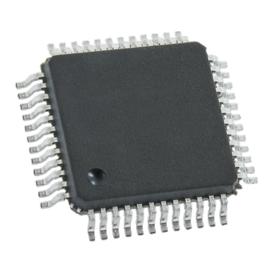
Pin name P40/SEG0 P41/SEG1 P42/SEG2 PD4/OSC4 PD3/OSC3 P43/SEG3 P17/UPMUX P44/SEG4 P16/FOUT/UPMUX S1C17M12 P45/SEG5 P15/EXCL01/UPMUX P46/SEG6 P14/EXCL00/UPMUX P47/SEG7 P13/EXOSC/UPMUX P12/UPMUX/EXSVD1 P50/REMO/COM0 P11/UPMUX/EXSVD0 P51/CLPLS/COM1 P10/UPMUX Figure 1.3.1.1 S1C17M12 Pin Configuration Diagram (TQFP12-48PIN) Seiko Epson Corporation S1C17M12/M13 TECHNICAL MANUAL (Rev. 1.2) - Page 17 Pin name P40/SEG0 P41/SEG1 P42/SEG2 PD4/OSC4 P43/SEG3 PD3/OSC3 P17/#ADTRG0/UPMUX P44/SEG4 P16/FOUT/UPMUX S1C17M13 P45/SEG5 P15/EXCL01/UPMUX P14/EXCL00/UPMUX P46/SEG6 P13/EXOSC/UPMUX P47/SEG7 P12/UPMUX/EXSVD1 P11/UPMUX/EXSVD0 P50/REMO/COM0 P51/CLPLS/COM1 P10/UPMUX/VREFA0 Figure 1.3.1.2 S1C17M13 Pin Configuration Diagram (TQFP12-48PIN) Seiko Epson Corporation S1C17M12/M13 TECHNICAL MANUAL (Rev. 1.2)
-
Page 18: Pad Configuration Diagram (Chip)
P10/UPMUX ∗1 ∗1 ∗1 2.28 mm Figure 1.3.2.1 S1C17M12 Pad Configuration Diagram (Chip) *1 These pads have the same specification. Select one pad to be used. Pad opening: X = 68 µm, Y = 68 µm Chip thickness: 400 µm... - Page 19 *1 These pads have the same specification. Select one pad to be used. Pad opening: X = 68 µm, Y = 68 µm Chip thickness: 400 µm Table 1.3.2.1 S1C17M12/M13 Pad Coordinates X µm Y µm X µm Y µm X µm...
-
Page 20: Pin Descriptions
External power supply voltage detection input Ch.0 ✓ ✓ – Hi-Z I/O port ✓ ✓ UPMUX User-selected I/O (universal port multiplexer) ✓ ✓ EXSVD1 External power supply voltage detection input Ch.1 ✓ ✓ Seiko Epson Corporation S1C17M12/M13 TECHNICAL MANUAL (Rev. 1.2) - Page 21 OSC3 oscillator circuit input ✓ ✓ – Hi-Z I/O port ✓ ✓ OSC4 OSC3 oscillator circuit output ✓ ✓ Note: In the peripheral circuit descriptions, the assigned signal name is used as the pin name. Seiko Epson Corporation S1C17M12/M13 TECHNICAL MANUAL (Rev. 1.2)
- Page 22 16-bit PWM timer (T16B) TOUTn0/CAPn0 n = 0 T16B Ch.n PWM output/capture input 0 TOUTn1/CAPn1 T16B Ch.n PWM output/capture input 1 Note: Do not assign a function to two or more pins simultaneously. Seiko Epson Corporation 1-10 S1C17M12/M13 TECHNICAL MANUAL (Rev. 1.2)
-
Page 23: Power Supply, Reset, And Clocks
“Recommended Operat- ing Conditions, Power supply voltage V ” in the “Electrical Characteristics” chapter and the “Basic Exter- nal Connection Diagram” chapter, respectively. Seiko Epson Corporation S1C17M12/M13 TECHNICAL MANUAL (Rev. 1.2) -
Page 24: D1 Regulator Operation Mode
To CPU and peripheral circuits Key-entry reset Watchdog timer reset Supply voltage detector reset SYSRST_S0_0 Software reset 0 To peripheral circuit 0 Reset decoder SYSRST_S0_n Software reset n To peripheral circuit n Figure 2.2.1.1 SRC Configuration Seiko Epson Corporation S1C17M12/M13 TECHNICAL MANUAL (Rev. 1.2) -
Page 25: Input Pin
Note, however, that the software reset operations depend on the periph- eral circuit. For more information, refer to “Control Registers” in each peripheral circuit chapter. Note: The MODEN bit of some peripheral circuits does not issue software reset. Seiko Epson Corporation S1C17M12/M13 TECHNICAL MANUAL (Rev. 1.2) -
Page 26: Initialization Conditions (Reset Groups)
- The oscillator and clock input circuit on/off state can be maintained or changed at SLEEP mode cancelation. • Provides the FOUT function to output an internal clock for driving external ICs or for monitoring the internal state. Figure 2.3.1.1 shows the CLG configuration. Seiko Epson Corporation S1C17M12/M13 TECHNICAL MANUAL (Rev. 1.2) -
Page 27: Input/Output Pins
Figure 2.3.3.1 IOSC Oscillator Circuit Configuration The IOSC oscillator circuit output clock IOSCCLK is used as SYSCLK at booting. For the oscillation charac- teristics, refer to “IOSC oscillator circuit characteristics” in the “Electrical Characteristics” chapter. Seiko Epson Corporation S1C17M12/M13 TECHNICAL MANUAL (Rev. 1.2) -
Page 28: Operations
The oscillation start time refers to the time after the oscillator circuit is enabled until the oscillation signal is ac- tually sent to the internal circuits. The oscillation stabilization waiting time refers to the time it takes the clock to stabilize after the oscillation starts. Seiko Epson Corporation S1C17M12/M13 TECHNICAL MANUAL (Rev. 1.2) - Page 29 6. When using the crystal/ceramic oscillator, assign the OSC3 oscillator input/output functions to the ports. (Refer to the “I/O Ports” chapter.) 7. Write 1 to the CLGOSC.OSC3EN bit. (Start oscillation) 8. OSC3CLK can be used if the CLGINTF.OSC3STAIF bit = 1 after an interrupt occurs. Seiko Epson Corporation S1C17M12/M13 TECHNICAL MANUAL (Rev. 1.2)
- Page 30 This allows flexible clock control according to the wake-up process. Configure the clock using the CLGSCLK.WUPSRC[1:0] and CLGSCLK.WUPDIV[1:0] bits, and write 1 to the CLGSCLK.WUPMD bit to enable this function. Seiko Epson Corporation S1C17M12/M13 TECHNICAL MANUAL (Rev. 1.2)
-
Page 31: Operating Mode
Note: The reset cancelation time at power-on varies according to the power rise time and reset request cancelation time. For the reset hold time t , refer to “Reset hold circuit characteristics” in the “Electrical Characteristics” chapter. RSTR Seiko Epson Corporation S1C17M12/M13 TECHNICAL MANUAL (Rev. 1.2) -
Page 32: Transition Between Operating Modes
CLGSCLK.CLKSRC[1:0] = 0x3 EXOSC OSC3 ∗ In RUN and HALT modes, the clock sources not used HALT HALT as SYSCLK can be all disabled. Figure 2.4.2.1 Operating Mode-to-Mode State Transition Diagram Seiko Epson Corporation 2-10 S1C17M12/M13 TECHNICAL MANUAL (Rev. 1.2) -
Page 33: Interrupts
Bit name Initial Reset Remarks CLGSCLK WUPMD R/WP – – – 13–12 WUPDIV[1:0] R/WP 11–10 – – 9–8 WUPSRC[1:0] R/WP 7–6 – – 5–4 CLKDIV[1:0] R/WP 3–2 – – 1–0 CLKSRC[1:0] R/WP Seiko Epson Corporation S1C17M12/M13 TECHNICAL MANUAL 2-11 (Rev. 1.2) - Page 34 When a currently stopped clock source is selected, it will automatically start oscillating or clock input. Table 2.6.3 SYSCLK Clock Source and Division Ratio Settings CLGSCLK.CLKSRC[1:0] bits CLGSCLK. CLKDIV[1:0] bits IOSCCLK Reserved OSC3CLK EXOSCCLK – 1/16 Reserved Seiko Epson Corporation 2-12 S1C17M12/M13 TECHNICAL MANUAL (Rev. 1.2)
-
Page 35: Clg Oscillation Control Register
9–8 OSC3MD[1:0] R/WP 7–6 – – 5–4 OSC3INV[1:0] R/WP – – 2–0 OSC3WT[2:0] R/WP Bits 15–12 Reserved Bits 11–10 OSC3FQ[1:0] These bits set the oscillation frequency of the OSC3 internal oscillator circuit. Seiko Epson Corporation S1C17M12/M13 TECHNICAL MANUAL 2-13 (Rev. 1.2) -
Page 36: Clg Interrupt Flag Register
Bit 0 IOSCSTAIF These bits indicate the CLG interrupt cause occurrence statuses. 1 (R): Cause of interrupt occurred 0 (R): No cause of interrupt occurred 1 (W): Clear flag 0 (W): Ineffective Seiko Epson Corporation 2-14 S1C17M12/M13 TECHNICAL MANUAL (Rev. 1.2) -
Page 37: Clg Interrupt Enable Register
1/64 1/64 1/32 1/32 1/16 1/16 Note: When the CLGFOUT.FOUTSRC[1:0] bits are set to 0x3, the FOUT output will be stopped in SLEEP/HALT mode as SYSCLK is stopped. Bit 1 Reserved Seiko Epson Corporation S1C17M12/M13 TECHNICAL MANUAL 2-15 (Rev. 1.2) - Page 38 0 (R/W): Disable external output Note: Since the FOUT signal generated is out of sync with writings to the CLGFOUT.FOUTEN bit, a glitch may occur when the FOUT output is enabled or disabled. Seiko Epson Corporation 2-16 S1C17M12/M13 TECHNICAL MANUAL (Rev. 1.2)
-
Page 39: Cpu And Debugger
3 CPU AND DEBUGGER 3 CPU and Debugger 3.1 Overview This IC incorporates the Seiko Epson original 16-bit CPU core (S1C17) with a debugger. The main features of the CPU core are listed below. • Seiko Epson original 16-bit RISC processor... -
Page 40: Cpu Core
DBRUN bit, refer to “Clock Supply in DEBUG Mode” in each peripheral circuit chapter. DE- BUG mode continues until a cancel command is sent from the personal computer or the CPU executes the retd in- struction. Neither hardware interrupts nor NMI are accepted during DEBUG mode. Seiko Epson Corporation S1C17M12/M13 TECHNICAL MANUAL (Rev. 1.2) -
Page 41: Resource Requirements And Debugging Tools
For the recommended pull-up resistor value, refer to “Recommended Operating Conditions, DSIO pull-up resis- tor R ” in the “Electrical Characteristics” chapter. R is not required when using the DSIO pin as a general- purpose I/O port pin. Seiko Epson Corporation S1C17M12/M13 TECHNICAL MANUAL (Rev. 1.2) -
Page 42: Flash Security Function
The value (0 or 1) of the PSR Z (zero) flag can be read out with this bit. Bit 0 PSRN The value (0 or 1) of the PSR N (negative) flag can be read out with this bit. Seiko Epson Corporation S1C17M12/M13 TECHNICAL MANUAL (Rev. 1.2) -
Page 43: Debug Ram Base Register
– 23–0 DBRAM[23:0] *1 Debugging work area start address Bits 31–24 Reserved Bits 23–0 DBRAM[23:0] The start address of the debugging work area (64 bytes) can be read out with these bits. Seiko Epson Corporation S1C17M12/M13 TECHNICAL MANUAL (Rev. 1.2) -
Page 44: Memory And Bus
Access size designated by the CPU instructions (e.g., ld %rd, [%rb] → 16-bit data transfer) Table 4.2.1 lists numbers of bus access cycles by different device size and access size. The peripheral circuits can be accessed with an 8-bit, 16-bit, or 32-bit instruction. Seiko Epson Corporation S1C17M12/M13 TECHNICAL MANUAL (Rev. 1.2) -
Page 45: Flash Memory
The number of bus access cycles for reading can be configured using the FLASHCWAIT.RDWAIT[1:0] bits. Select a setting for higher frequency than the system clock. Seiko Epson Corporation S1C17M12/M13 TECHNICAL MANUAL (Rev. 1.2) -
Page 46: Flash Programming
CLG System Clock Control Register 0x4042 CLGOSC CLG Oscillation Control Register 0x4048 CLGOSC3 CLG OSC3 Control Register 0x404c CLGINTF CLG Interrupt Flag Register 0x404e CLGINTE CLG Interrupt Enable Register 0x4050 CLGFOUT CLG FOUT Control Register Seiko Epson Corporation S1C17M12/M13 TECHNICAL MANUAL (Rev. 1.2) - Page 47 0x4250 P5DAT P5 Port Data Register 0x4252 P5IOEN P5 Port Enable Register 0x4254 P5RCTL P5 Port Pull-up/down Control Register 0x4256 P5INTF P5 Port Interrupt Flag Register 0x4258 P5INTCTL P5 Port Interrupt Control Register Seiko Epson Corporation S1C17M12/M13 TECHNICAL MANUAL (Rev. 1.2)
- Page 48 0x5010 T16B0CCCTL0 T16B Ch.0 Compare/Capture 0 Control Register 0x5012 T16B0CCR0 T16B Ch.0 Compare/Capture 0 Data Register 0x5018 T16B0CCCTL1 T16B Ch.0 Compare/Capture 1 Control Register 0x501a T16B0CCR1 T16B Ch.0 Compare/Capture 1 Data Register Seiko Epson Corporation S1C17M12/M13 TECHNICAL MANUAL (Rev. 1.2)
-
Page 49: System-Protect Function
Note: Once write protection is removed using the MSCPROT.PROT[15:0] bits, write enabled status is maintained until write protection is applied again. After the registers/bits required have been al- tered, apply write protection. Seiko Epson Corporation S1C17M12/M13 TECHNICAL MANUAL (Rev. 1.2) -
Page 50: Control Registers
FLASHCWAIT.RDWAIT[1:0] bits Number of bus Access cycles System clock frequency 16.8 MHz (max.) 16.8 MHz (max.) 12.6 MHz (max.) 6.3 MHz (max.) Note: Be sure to set the FLASHCWAIT.RDWAIT[1:0] bits before the system clock is configured. Seiko Epson Corporation S1C17M12/M13 TECHNICAL MANUAL (Rev. 1.2) -
Page 51: Interrupt Controller (Itc)
Address misaligned interrupt Memory access instruction – (0xfffc00) Debugging interrupt brk instruction, etc. 2 (0x02) TTBR + 0x08 Watchdog timer overflow 3 (0x03) TTBR + 0x0c Reserved for C compiler – – Seiko Epson Corporation S1C17M12/M13 TECHNICAL MANUAL (Rev. 1.2) -
Page 52: Vector Table Base Address (Ttbr)
Bits 7 to 0 in the MSCTTBRL register are fixed at 0, so the vector table always begins from a 256-byte boundary address. Seiko Epson Corporation S1C17M12/M13 TECHNICAL MANUAL (Rev. 1.2) -
Page 53: Initialization
The previously occurring interrupt is held. The held interrupt is canceled and no interrupt is generated if the interrupt flag in the peripheral circuit is cleared via software. Seiko Epson Corporation S1C17M12/M13 TECHNICAL MANUAL (Rev. 1.2) -
Page 54: Conditions To Accept Interrupt Requests By The Cpu
Note: When HALT or SLEEP mode is canceled, the CPU jumps to the interrupt handler routine after executing one instruction. To execute the interrupt handler routine immediately after HALT or SLEEP mode is canceled, place the nop instruction at just behind the halt/slp instruction. Seiko Epson Corporation S1C17M12/M13 TECHNICAL MANUAL (Rev. 1.2) -
Page 55: Control Registers
Setup Register 1) 7–0 – 0x00 – – ITCLV2 15–11 – 0x00 – – (ITC Interrupt Level 10–8 ILV5[2:0] 16-bit timer Ch.0 interrupt (ILVT16_0) Setup Register 2) 7–0 – 0x00 – – Seiko Epson Corporation S1C17M12/M13 TECHNICAL MANUAL (Rev. 1.2) - Page 56 2–0 ILV14[2:0] 12-bit A/D converter interrupt (ILVADC12_0) ITCLV8 15–8 – 0x00 – – (ITC Interrupt Level 7–3 – 0x00 – – Setup Register 8) 2–0 ILV16[2:0] Synchronous serial interface Ch.1 interrupt (ILVSPIA_1) Seiko Epson Corporation S1C17M12/M13 TECHNICAL MANUAL (Rev. 1.2)
-
Page 57: O Ports (Pport)
Note: ‘x’, which is used in the port names Pxy, register names, and bit names, refers to a port group (x = 0, 1, 2, ··· , d) and ‘y’ refers to a port number (y = 0, 1, 2, ··· , 7). Figure 6.1.1 shows the configuration of PPORT. Table 6.1.1 Port Configuration of S1C17M12/M13 Item S1C17M12... -
Page 58: I/O Cell Structure And Functions
Falling time (port level = high → low) [second] High level Schmitt input threshold voltage [V] Low level Schmitt input threshold voltage [V] : Pull-up/pull-down resistance [W] Pin capacitance [F] Parasitic capacitance on the board [F] BOARD Seiko Epson Corporation S1C17M12/M13 TECHNICAL MANUAL (Rev. 1.2) -
Page 59: Cmos Output And High Impedance State
However, the control registers can be altered. If the PCLK.DBRUN bit = 1, the CLK_ PPORT supply is not suspended and the chattering filter will keep operating in DEBUG mode. Seiko Epson Corporation S1C17M12/M13 TECHNICAL MANUAL (Rev. 1.2) -
Page 60: Operations
- Set the PxRCTL.PxRENy bit to 1. (Enable pull-up/down) Set the PxRCTL.PxRENy bit to 0 if the internal pull-up/down resistors are not used. 4. Set the PxMODSEL.PxSELy bit to 0. (Enable GPIO function) Seiko Epson Corporation S1C17M12/M13 TECHNICAL MANUAL (Rev. 1.2) -
Page 61: Port Input/Output Control
2 to 3 Input sampling time = — — — — — — — — — — — — — — — — [second] (Eq.6.2) CLK_PPORT frequency [Hz] Seiko Epson Corporation S1C17M12/M13 TECHNICAL MANUAL (Rev. 1.2) -
Page 62: Interrupts
Clearing the PxINTF.PxIFy bit also clears the PINTFGRP. PxINT bit. If the port is set to interrupt disabled status by the PxINTCTL.PxIEy bit, the PINTFGRP.PxINT bit will not be set even if the PxINTF.PxIFy bit is set to 1. Seiko Epson Corporation S1C17M12/M13 TECHNICAL MANUAL (Rev. 1.2) -
Page 63: Px Port Data Register
Initial Reset Remarks PxRCTL 15–8 PxPDPU[7:0] 0x00 – 7–0 PxREN[7:0] 0x00 *1: This register is effective when the GPIO function is selected. *2: The bit configuration differs depending on the port group. Seiko Epson Corporation S1C17M12/M13 TECHNICAL MANUAL (Rev. 1.2) -
Page 64: Px Port Interrupt Flag Register
Px Port Chattering Filter Enable Register Register name Bit name Initial Reset Remarks PxCHATEN 15–8 – 0x00 – – 7–0 PxCHATEN[7:0] 0x00 *1: The bit configuration differs depending on the port group. Seiko Epson Corporation S1C17M12/M13 TECHNICAL MANUAL (Rev. 1.2) -
Page 65: Px Port Mode Select Register
P Port Clock Control Register Register name Bit name Initial Reset Remarks PCLK 15–9 – 0x00 – – DBRUN R/WP 7–4 CLKDIV[3:0] R/WP 3–2 KRSTCFG[1:0] R/WP 1–0 CLKSRC[1:0] R/WP Bits 15–9 Reserved Seiko Epson Corporation S1C17M12/M13 TECHNICAL MANUAL (Rev. 1.2) - Page 66 1/32,768 1/16,384 1/8,192 1/4,096 1/2,048 1/1,024 1/512 1/256 1/128 1/64 1/32 1/16 (Note) The oscillation circuits/external input that are not supported in this IC cannot be selected as the clock source. Seiko Epson Corporation 6-10 S1C17M12/M13 TECHNICAL MANUAL (Rev. 1.2)
-
Page 67: P Port Interrupt Flag Group Register
A port generated an interrupt 0 (R): No port generated an interrupt The PINTFGRP.PxINT bit is cleared when the interrupt flag for the port that has generated an interrupt is cleared. Seiko Epson Corporation S1C17M12/M13 TECHNICAL MANUAL 6-11 (Rev. 1.2) -
Page 68: Control Register And Port Function Configuration Of This Ic
– – – UPMUX ADC12A ADIN1 *2 – – – – UPMUX ADC12A ADIN0 *2 – – *1: Refer to the “Universal Port Multiplexer” chapter. *2: Available only in the S1C17M13. Seiko Epson Corporation 6-12 S1C17M12/M13 TECHNICAL MANUAL (Rev. 1.2) -
Page 69: P1 Port Group
– – – FOUT UPMUX – – – – ADC12A #ADTRG0 *2 UPMUX – – – – *1: Refer to the “Universal Port Multiplexer” chapter. *2: Available only in the S1C17M13. Seiko Epson Corporation S1C17M12/M13 TECHNICAL MANUAL 6-13 (Rev. 1.2) -
Page 70: P2 Port Group
– – – – UPMUX – – – – – – UPMUX – – – – – – UPMUX – – – – *1: Refer to the “Universal Port Multiplexer” chapter. Seiko Epson Corporation 6-14 S1C17M12/M13 TECHNICAL MANUAL (Rev. 1.2) -
Page 71: P4 Port Group
– LEDC SEG4 – – – – – – LEDC SEG5 – – – – – – LEDC SEG6 – – – – – – LEDC SEG7 – – – – Seiko Epson Corporation S1C17M12/M13 TECHNICAL MANUAL 6-15 (Rev. 1.2) -
Page 72: P5 Port Group
CLPLS LEDC COM1 – – – – – – LEDC COM2 – – – – – – LEDC COM3 – – – – – – LEDC COM4 – – – – Seiko Epson Corporation 6-16 S1C17M12/M13 TECHNICAL MANUAL (Rev. 1.2) -
Page 73: Pd Port Group
– – – DSIO – – – – – – DCLK – – – – – – – – – – OSC3 – – – – – – OSC4 – – Seiko Epson Corporation S1C17M12/M13 TECHNICAL MANUAL 6-17 (Rev. 1.2) -
Page 74: Common Registers Between Port Groups
7–4 CLKDIV[3:0] R/WP 3–2 KRSTCFG[1:0] R/WP 1–0 CLKSRC[1:0] R/WP PINTFGRP 15–8 – 0x00 – – (P Port Interrupt Flag 7–6 – – Group Register) P5INT P4INT – – P2INT P1INT P0INT Seiko Epson Corporation 6-18 S1C17M12/M13 TECHNICAL MANUAL (Rev. 1.2) -
Page 75: Universal Port Multiplexer (Upmux)
4. Initialize the peripheral circuit. 5. Set the PxFNCSEL.PxyMUX[1:0] bits of the I/O port to 0x1. (Select peripheral I/O function 1) 6. Set the PxMODSEL.PxSELy bit of the I/O port to 1. (Enable peripheral I/O function) Seiko Epson Corporation S1C17M12/M13 TECHNICAL MANUAL (Rev. 1.2) -
Page 76: Control Registers
Note: Do not assign a peripheral input function to two or more I/O ports. Although the I/O ports output the same waveforms when an output function is assigned to two or more I/O port, a skew oc- curs due to the internal delay. Seiko Epson Corporation S1C17M12/M13 TECHNICAL MANUAL (Rev. 1.2) -
Page 77: Watchdog Timer (Wdt2)
CLK_WDT2 supply is suspended, the register retains the status before DEBUG mode was entered. If the WDTCLK.DBRUN bit = 1, the CLK_WDT2 supply is not suspended and WDT2 will keep operating in DE- BUG mode. Seiko Epson Corporation S1C17M12/M13 TECHNICAL MANUAL (Rev. 1.2) -
Page 78: Operations
1. Write 0x0096 to the MSCPROT.PROT[15:0] bits. (Remove system protection) 2. Write 0xa to the WDTCTL.WDTRUN[3:0] bits. (Stop WDT2) 3. Write a value other than 0x0096 to the MSCPROT.PROT[15:0] bits. (Set system protection) Seiko Epson Corporation S1C17M12/M13 TECHNICAL MANUAL (Rev. 1.2) -
Page 79: Operations In Halt And Sleep Modes
IOSC OSC1 OSC3 EXOSC 1/65,536 1/128 1/65,536 1/32,768 1/32,768 1/16,384 1/16,384 1/8,192 1/8,192 (Note) The oscillation circuits/external input that are not supported in this IC cannot be selected as the clock source. Seiko Epson Corporation S1C17M12/M13 TECHNICAL MANUAL (Rev. 1.2) -
Page 80: Wdt2 Control Register
WDT2 should also be reset concurrently when running WDT2. WDT2 Counter Compare Match Register Register name Bit name Initial Reset Remarks WDTCMP 15–10 – 0x00 – – 9–0 CMP[9:0] 0x3ff R/WP Bits 15–10 Reserved Seiko Epson Corporation S1C17M12/M13 TECHNICAL MANUAL (Rev. 1.2) - Page 81 These bits set the NMI/reset generation cycle. The value set in this register is compared with the 10-bit counter value while WDT2 is running, and an NMI or reset is generated when they are matched. Seiko Epson Corporation S1C17M12/M13 TECHNICAL MANUAL (Rev. 1.2)
-
Page 82: Supply Voltage Detector (Svd3)
- Continuous operation is also possible. Figure 9.1.1 shows the configuration of SVD3. Table 9.1.1 SVD3 Configuration of S1C17M12/M13 Item S1C17M12 S1C17M12 Power supply voltage to be detected... -
Page 83: Input Pins And External Connection
SLEEP mode and SVD3 stops with the register settings maintained at those before entering SLEEP mode. After the CPU returns to normal mode, CLK_SVD3 is supplied and the SVD3 operation resumes. Seiko Epson Corporation S1C17M12/M13 TECHNICAL MANUAL (Rev. 1.2) -
Page 84: Clock Supply In Debug Mode
SVDCTL.MODEN bit = 1, wait for at least SVD circuit response time SVD_EXT before reading the SVDINTF.SVDDT bit (refer to “Supply Voltage Detector Characteristics, SVD circuit re- sponse time t ” in the “Electrical Characteristics” chapter). Seiko Epson Corporation S1C17M12/M13 TECHNICAL MANUAL (Rev. 1.2) -
Page 85: Svd3 Operations
SVDIF bit). An interrupt request is sent to the interrupt controller only when the SVDINTF.SVDIF bit is set while the interrupt is enabled by the SVDINTE.SVDIE bit. For more information on interrupt control, refer to the “Interrupt Controller” chapter. Seiko Epson Corporation S1C17M12/M13 TECHNICAL MANUAL (Rev. 1.2) -
Page 86: Svd3 Reset
0 (R/WP): No clock supplied in DEBUG mode Bit 7 Reserved Bits 6–4 CLKDIV[2:0] These bits select the division ratio of the SVD3 operating clock. Bits 3–2 Reserved Bits 1–0 CLKSRC[1:0] These bits select the clock source of SVD3. Seiko Epson Corporation S1C17M12/M13 TECHNICAL MANUAL (Rev. 1.2) -
Page 87: Svd3 Control Register
0x02 0x01 ↓ 0x00 For the configurable range and voltage values, refer to “Supply Voltage Detector Characteristics, SVD detection voltage V /EXSVD detection voltage V ” in the “Electrical Characteristics” chapter. SVD_EXT Seiko Epson Corporation S1C17M12/M13 TECHNICAL MANUAL (Rev. 1.2) -
Page 88: Svd3 Status And Interrupt Flag Register
EXSVD0/1) < SVD detection voltage V or EXSVD detection voltage V SVD_EXT 0 (R): Power supply voltage (V or EXSVD0/1) ≥ SVD detection voltage V or EXSVD detection voltage V SVD_EXT Bits 7–1 Reserved Seiko Epson Corporation S1C17M12/M13 TECHNICAL MANUAL (Rev. 1.2) -
Page 89: Svd3 Interrupt Enable Register
Notes: • If the SVDCTL.SVDRE[3:0] bits are set to 0xa, no low power supply voltage detection interrupt will occur, as a reset is issued at the same timing as an interrupt. • To prevent generating unnecessary interrupts, the corresponding interrupt flag should be cleared before enabling interrupts. Seiko Epson Corporation S1C17M12/M13 TECHNICAL MANUAL (Rev. 1.2) -
Page 90: 16-Bit Timers (T16)
• A clock source and clock division ratio for generating the count clock are selectable. • Repeat mode or one-shot mode is selectable. • Can generate counter underflow interrupts. Figure 10.1.1 shows the configuration of a T16 channel. Table 10.1.1 T16 Channel Configuration of S1C17M12/M13 Item S1C17M12 S1C17M13 Number of channels 4 channels (Ch.0–Ch.3) -
Page 91: Clock Settings
(Set reload data (counter preset data)) 5. Set the following bits when using the interrupt: - Write 1 to the T16_nINTF.UFIF bit. (Clear interrupt flag) - Set the T16_nINTE.UFIE bit to 1. (Enable underflow interrupt) Seiko Epson Corporation 10-2 S1C17M12/M13 TECHNICAL MANUAL (Rev. 1.2) -
Page 92: Counter Underflow
At the same time the counter stops, the T16_ nCTL.PRUN bit is cleared automatically. Select this mode to stop the counter after an interrupt has occurred once, such as for checking a specific lapse of time. Seiko Epson Corporation S1C17M12/M13 TECHNICAL MANUAL 10-3 (Rev. 1.2) -
Page 93: Counter Value Read
Bits 7–4 CLKDIV[3:0] These bits select the division ratio of the T16 Ch.n operating clock (counter clock). Bits 3–2 Reserved Bits 1–0 CLKSRC[1:0] These bits select the clock source of T16 Ch.n. Seiko Epson Corporation 10-4 S1C17M12/M13 TECHNICAL MANUAL (Rev. 1.2) -
Page 94: T16 Ch.n Control Register
PRESET MODEN Bits 15–9 Reserved Bit 8 PRUN This bit starts/stops the timer. 1 (W): Start timer 0 (W): Stop timer 1 (R): Timer is running 0 (R): Timer is idle Seiko Epson Corporation S1C17M12/M13 TECHNICAL MANUAL 10-5 (Rev. 1.2) -
Page 95: T16 Ch.n Reload Data Register
This bit indicates the T16 Ch.n underflow interrupt cause occurrence status. 1 (R): Cause of interrupt occurred 0 (R): No cause of interrupt occurred 1 (W): Clear flag 0 (W): Ineffective Seiko Epson Corporation 10-6 S1C17M12/M13 TECHNICAL MANUAL (Rev. 1.2) -
Page 96: T16 Ch.n Interrupt Enable Register
This bit enables T16 Ch.n underflow interrupts. 1 (R/W): Enable interrupts 0 (R/W): Disable interrupts Note: To prevent generating unnecessary interrupts, the corresponding interrupt flag should be cleared before enabling interrupts. Seiko Epson Corporation S1C17M12/M13 TECHNICAL MANUAL 10-7 (Rev. 1.2) -
Page 97: Uart (Uart3)
• Input pin can be pulled up with an internal resistor. • The output pin is configurable as an open-drain output. • Provides the carrier modulation output function. Figure 11.1.1 shows the UART3 configuration. Table 11.1.1 UART3 Channel Configuration of S1C17M12/M13 Item S1C17M12 S1C17M13 Number of channels 1 channel (Ch.0) -
Page 98: Input/Output Pins And External Connections
- UAnCLK.CLKSRC[1:0] bits (Clock source selection) - UAnCLK.CLKDIV[1:0] bits (Clock division ratio selection = Clock frequency setting) The UART3 operating clock should be selected so that the baud rate generator will be configured easily. Seiko Epson Corporation 11-2 S1C17M12/M13 TECHNICAL MANUAL (Rev. 1.2) -
Page 99: Clock Supply In Sleep Mode
(UAnMOD.STPB bit = 1). Parity function The parity function is configured using the UAnMOD.PREN and UAnMOD.PRMD bits. Table 11.4.1 Parity Function Setting UAnMOD.PREN bit UAnMOD.PRMD bit Parity function Odd parity Even parity Non parity Seiko Epson Corporation S1C17M12/M13 TECHNICAL MANUAL 11-3 (Rev. 1.2) -
Page 100: Operations
- Set the interrupt enable bits in the UAnINTE register to 1. * (Enable interrupts) * The initial value of the UAnINTF.TBEIF bit is 1, therefore, an interrupt will occur immediately after the UA- nINTE.TBEIE bit is set to 1. Seiko Epson Corporation 11-4 S1C17M12/M13 TECHNICAL MANUAL (Rev. 1.2) -
Page 101: Data Transmission
Read the UAnINTF.TBEIF bit UAnINTF.TBEIF = 1 ? Write transmit data to the UAnTXD register Transmit data remained? Wait for an interrupt request (UAnINTF.TBEIF = 1) Figure 11.5.2.2 Data Transmission Flowchart Seiko Epson Corporation S1C17M12/M13 TECHNICAL MANUAL 11-5 (Rev. 1.2) -
Page 102: Data Reception
Read receive data (1 byte) from the UAnRXD register the UAnRXD register Read receive data (1 byte) from the UAnRXD register Receive data remained? Receive data remained? Figure 11.5.3.2 Data Reception Flowcharts Seiko Epson Corporation 11-6 S1C17M12/M13 TECHNICAL MANUAL (Rev. 1.2) -
Page 103: Irda Interface
Writing 1 to the UAnMOD.CAREN bit enables the carrier modulation function allowing carrier modulation wave- forms to be output according to the UAnMOD.PECAR bit setting. Data transmit control is identical to that for nor- mal interface even in this case. Seiko Epson Corporation S1C17M12/M13 TECHNICAL MANUAL 11-7 (Rev. 1.2) -
Page 104: Receive Errors
The received data that encountered an error is still transferred to the receive data buffer and the UAnINTF.PEIF bit (parity error interrupt flag) is set to 1 when the data becomes ready to read from the UAnRXD register (see the Note on framing error). Seiko Epson Corporation 11-8 S1C17M12/M13 TECHNICAL MANUAL (Rev. 1.2) -
Page 105: Overrun Error
1 (R/W): Clock supplied in DEBUG mode 0 (R/W): No clock supplied in DEBUG mode Bits 7–6 Reserved Bits 5–4 CLKDIV[1:0] These bits select the division ratio of the UART3 operating clock. Bits 3–2 Reserved Seiko Epson Corporation S1C17M12/M13 TECHNICAL MANUAL 11-9 (Rev. 1.2) -
Page 106: Uart3 Ch.n Mode Register
0 (R/W): Disable input inverting function Bit 8 INVTX This bit enables the USOUTn output inverting function. 1 (R/W): Enable output inverting function 0 (R/W): Disable output inverting function Bit 7 Reserved Seiko Epson Corporation 11-10 S1C17M12/M13 TECHNICAL MANUAL (Rev. 1.2) -
Page 107: Uart3 Ch.n Baud-Rate Register
Notes: • The UAnBR register settings can be altered only when the UAnCTL.MODEN bit = 0. • Do not set the UAnBR.FMD[3:0] bits to a value other than 0 to 3 when the UAnMOD.BRDIV bit = 1. Seiko Epson Corporation S1C17M12/M13 TECHNICAL MANUAL 11-11 (Rev. 1.2) -
Page 108: Uart3 Ch.n Control Register
Bits 15–8 Reserved Bits 7–0 RXD[7:0] The receive data buffer can be read through these bits. The receive data buffer consists of a 2-byte FIFO, and older received data is read first. Seiko Epson Corporation 11-12 S1C17M12/M13 TECHNICAL MANUAL (Rev. 1.2) -
Page 109: Uart3 Ch.n Status And Interrupt Flag Register
UAnINTF.PEIF bit: Parity error interrupt UAnINTF.OEIF bit: Overrun error interrupt UAnINTF.RB2FIF bit: Receive buffer two bytes full interrupt UAnINTF.RB1FIF bit: Receive buffer one byte full interrupt UAnINTF.TBEIF bit: Transmit buffer empty interrupt Seiko Epson Corporation S1C17M12/M13 TECHNICAL MANUAL 11-13 (Rev. 1.2) -
Page 110: Uart3 Ch.n Interrupt Enable Register
UAnCAWF 15–8 – 0x00 – – 7–0 CRPER[7:0] 0x00 Bits 15–8 Reserved Bits 7–0 CRPER[7:0] These bits set the carrier modulation output frequency. For more information, refer to “Carrier Modu- lation.” Seiko Epson Corporation 11-14 S1C17M12/M13 TECHNICAL MANUAL (Rev. 1.2) -
Page 111: Synchronous Serial Interface (Spia)
• Slave mode is capable of being operated in SLEEP mode allowing wake-up by an SPIA interrupt. • Input pins can be pulled up/down with an internal resistor. Figure 12.1.1 shows the SPIA configuration. Table 12.1.1 SPIA Channel Configuration of S1C17M12/M13 Item S1C17M12... -
Page 112: Input/Output Pins And External Connections
SDIn #SPISS0 SPICLKn #SPISS1 #SPISS #SPISS2 External SPI master device External SPI slave devices SPICLK SPICLK #SPISS SPICLK Figure 12.2.2.2 Connections between SPIA in Slave Mode and External SPI Master Device Seiko Epson Corporation 12-2 S1C17M12/M13 TECHNICAL MANUAL (Rev. 1.2) -
Page 113: Pin Functions In Master Mode And Slave Mode
16-bit timer channel and converts it to the SPICLKn. The 16-bit timer must be run with an appro- priate reload data set. The SPICLKn frequency (baud rate) and the 16-bit timer reload data are calculated by the equations shown below. Seiko Epson Corporation S1C17M12/M13 TECHNICAL MANUAL 12-3 (Rev. 1.2) -
Page 114: Clock Supply In Debug Mode
SDIn SDOn (Master mode) SDOn (Slave mode) SDOn (Slave mode) Writing data to the SPInTXD register Figure 12.3.3.1 SPI Clock Phase and Polarity (SPInMOD.LSBFST bit = 0, SPInMOD.CHLN[3:0] bits = 0x7) Seiko Epson Corporation 12-4 S1C17M12/M13 TECHNICAL MANUAL (Rev. 1.2) -
Page 115: Data Format
1. Assert the slave select signal by controlling the general-purpose output port (if necessary). 2. Check to see if the SPInINTF.TBEIF bit is set to 1 (transmit buffer empty). 3. Write transmit data to the SPInTXD register. Seiko Epson Corporation S1C17M12/M13 TECHNICAL MANUAL 12-5 (Rev. 1.2) - Page 116 SPInTXD register Transmit data remained? Wait for an interrupt request (SPInINTF.TBEIF = 1) Negate the slave select signal output from a general-purpose port Figure 12.5.2.2 Data Transmission Flowchart in Master Mode Seiko Epson Corporation 12-6 S1C17M12/M13 TECHNICAL MANUAL (Rev. 1.2)
-
Page 117: Data Reception In Master Mode
Software operations SPInRXD → Data (R) Data (W) → SPInTXD SPInRXD → Data (R) 1 (W) → SPInINTF.TENDIF Figure 12.5.3.1 Example of Data Receiving Operations in Master Mode (SPInMOD.CHLN[3:0] bits = 0x7) Seiko Epson Corporation S1C17M12/M13 TECHNICAL MANUAL 12-7 (Rev. 1.2) -
Page 118: Terminating Data Transfer In Master Mode
SPInTXD register data written is completed. If no transmit data is written during this period, the data bits input from the SDIn pin are shifted and output from the SDOn pin without being modified. Seiko Epson Corporation 12-8 S1C17M12/M13 TECHNICAL MANUAL (Rev. 1.2) - Page 119 Data (W) → SPInTXD Data (W) → SPInTXD Software operations SPInRXD → Data (R) SPInRXD → Data (R) Figure 12.5.5.1 Example of Data Transfer Operations in Slave Mode (SPInMOD.CHLN[3:0] bits = 0x7) Seiko Epson Corporation S1C17M12/M13 TECHNICAL MANUAL 12-9 (Rev. 1.2)
-
Page 120: Terminating Data Transfer In Slave Mode
“Interrupt Controller” chapter. The SPInINTF register also contains the BSY bit that indicates the SPIA operating status. Figure 12.6.1 shows the SPInINTF.BSY and SPInINTF.TENDIF bit set timings. Seiko Epson Corporation 12-10 S1C17M12/M13 TECHNICAL MANUAL (Rev. 1.2) -
Page 121: Control Registers
Remarks SPInMOD 15–12 – – – 11–8 CHLN[3:0] 7–6 – – PUEN NOCLKDIV LSBFST CPHA CPOL Bits 15–12 Reserved Bits 11–8 CHLN[3:0] These bits set the bit length of transfer data. Seiko Epson Corporation S1C17M12/M13 TECHNICAL MANUAL 12-11 (Rev. 1.2) -
Page 122: Spia Ch.n Control Register
Note: The SPInMOD register settings can be altered only when the SPInCTL.MODEN bit = 0. SPIA Ch.n Control Register Register name Bit name Initial Reset Remarks SPInCTL 15–8 – 0x00 – – 7–2 – 0x00 – SFTRST MODEN Bits 15–2 Reserved Seiko Epson Corporation 12-12 S1C17M12/M13 TECHNICAL MANUAL (Rev. 1.2) -
Page 123: Spia Ch.n Transmit Data Register
0x00 – – 6–4 – – OEIF H0/S0 Cleared by writing 1. TENDIF H0/S0 RBFIF H0/S0 Cleared by reading the SPInRXD register. TBEIF H0/S0 Cleared by writing to the SPInTXD register. Seiko Epson Corporation S1C17M12/M13 TECHNICAL MANUAL 12-13 (Rev. 1.2) -
Page 124: Spia Ch.n Interrupt Enable Register
The following shows the correspondence between the bit and interrupt: SPInINTE.OEIE bit: Overrun error interrupt SPInINTE.TENDIE bit: End-of-transmission interrupt SPInINTE.RBFIE bit: Receive buffer full interrupt SPInINTE.TBEIE bit: Transmit buffer empty interrupt Seiko Epson Corporation 12-14 S1C17M12/M13 TECHNICAL MANUAL (Rev. 1.2) -
Page 125: C (I2C)
• The input filter for the SDA and SCL inputs does not comply with the standard for removing noise spikes less than 50 ns. Figure 13.1.1 shows the I2C configuration. Table 13.1.1 I2C Channel Configuration of S1C17M12/M13 Item S1C17M12 S1C17M13 Number of channels 1 channel (Ch.0) -
Page 126: Input/Output Pins And External Connections
• The internal pull-up resistors for the I/O ports cannot be used for pulling up SDA and SCL. • When the I2C is set into master mode, no other master device can be connected to the I bus. Seiko Epson Corporation 13-2 S1C17M12/M13 TECHNICAL MANUAL (Rev. 1.2) -
Page 127: Clock Settings
13.3.3.1). Note: The I C bus transfer rate is limited to 100 kbit/s in standard mode or 400 kbit/s in fast mode. Do not set a transfer rate exceeding the limit. Seiko Epson Corporation S1C17M12/M13 TECHNICAL MANUAL 13-3 (Rev. 1.2) -
Page 128: Operations
- Set the I2CnCTL.MST bit to 0. (Set slave mode) - Set the I2CnCTL.SFTRST bit to 1. (Execute software reset) - Set the I2CnCTL.MODEN bit to 1. (Enable I2C Ch.n operations) Seiko Epson Corporation 13-4 S1C17M12/M13 TECHNICAL MANUAL (Rev. 1.2) -
Page 129: Data Transmission In Master Mode
I2CnINTF.NACKIF bit = 1 (NACK received), the I2C Ch.n generates a repeated START condition. When the repeated START condition has been generated, the I2CnINTF.STARTIF and I2CnINTF.TBEIF bits are both set to 1 same as when a START condition has been generated. Seiko Epson Corporation S1C17M12/M13 TECHNICAL MANUAL 13-5 (Rev. 1.2) - Page 130 Last data sent? Retry? Write 1 to the I2CnCTL.TXSTOP bit Write data to the I2CnTXD register Wait for an interrupt request (I2CnINTF.STOPIF = 1) Figure 13.4.2.2 Master Mode Data Transmission Flowchart Seiko Epson Corporation 13-6 S1C17M12/M13 TECHNICAL MANUAL (Rev. 1.2)
-
Page 131: Data Reception In Master Mode
This reading triggers the I2C Ch.n to start subsequent data reception. Generating a STOP or repeated START condition It is the same as the data transmission in master mode. Seiko Epson Corporation S1C17M12/M13 TECHNICAL MANUAL 13-7 (Rev. 1.2) - Page 132 Read receive data from the I2CnRXD register Write 1 to the I2CnCTL.TXSTOP bit Write 1 to the I2CnCTL.TXSTOP bit Wait for an interrupt request (I2CnINTF.STOPIF = 1) Figure 13.4.3.2 Master Mode Data Reception Flowchart Seiko Epson Corporation 13-8 S1C17M12/M13 TECHNICAL MANUAL (Rev. 1.2)
-
Page 133: 10-Bit Addressing In Master Mode
Clear the I2CnINTF.STARTIF bit by writing 1 after the interrupt has occurred. 9. Write the first address to the I2CnTXD.TXD[7:1] bits and 1 that represents READ as the data transfer direc- tion to the I2CnTXD.TXD0 bit. 10. Perform data reception. Seiko Epson Corporation S1C17M12/M13 TECHNICAL MANUAL 13-9 (Rev. 1.2) -
Page 134: Data Transmission In Slave Mode
Go to Step 6 when a STOP condition interrupt has occurred. ii. Go to Step 2 when a START condition interrupt has occurred. 6. Clear the I2CnINTF.STOPIF bit and then terminate data sending operations. Seiko Epson Corporation 13-10 S1C17M12/M13 TECHNICAL MANUAL (Rev. 1.2) - Page 135 A: ACK, A: NACK, Saddr/R: Slave address + R(1), Saddr/W: Slave address + W(0), STARTIF = 1 Data n: 8-bit data Figure 13.4.5.1 Example of Data Sending Operations in Slave Mode Seiko Epson Corporation S1C17M12/M13 TECHNICAL MANUAL 13-11 (Rev. 1.2)
-
Page 136: Data Reception In Slave Mode
I2C Ch.n sends an ACK and pulls down SCL to low. The received data in the shift register is transferred to the receive data buffer and the I2CnINTF.RBFIF and I2CnINTF.BYTEENDIF bits are both set to 1. Af- ter that, the received data can be read out from the I2CnRXD register. Seiko Epson Corporation 13-12 S1C17M12/M13 TECHNICAL MANUAL (Rev. 1.2) - Page 137 Wait for an interrupt request (I2CnINTF.RBFIF = 1) Last data received next? Write 1 to the I2CnCTL.TXNACK bit Read receive data from the I2CnRXD register Last data received? Figure 13.4.6.2 Slave Mode Data Reception Flowchart Seiko Epson Corporation S1C17M12/M13 TECHNICAL MANUAL 13-13 (Rev. 1.2)
-
Page 138: Slave Operations In 10-Bit Address Mode
If SDA does not change from low when the I2C Ch.n outputs the ninth clock, it is regarded as an automatic bus clearing failure. In this case, the I2C Ch.n clears the I2CnCTL.TXSTART bit to 0 and sets both the I2CnINTF.ERRIF and I2CnINTF.STARTIF bits to 1. Seiko Epson Corporation 13-14 S1C17M12/M13 TECHNICAL MANUAL (Rev. 1.2) -
Page 139: Error Detection
4 <Master mode only> When 1 is written to the I2CnCTL.TX- I2CnINTF.ERRIF = 1 START bit while the I2CnINTF.BSY bit = 0 (Refer to “Automatic Automatic bus clearing I2CnCTL.TXSTART = 0 Bus Clearing Operation.”) failure I2CnINTF.STARTIF = 1 Seiko Epson Corporation S1C17M12/M13 TECHNICAL MANUAL 13-15 (Rev. 1.2) -
Page 140: Interrupts
Master mode BRT + 3 CLK_I2Cn TXSTART = 1 TXSTART = 0 STARTIF = 1 Slave mode Address matching the I2CnOADR register BSY = 1 TR = 0/1 STARTIF = 1 Seiko Epson Corporation 13-16 S1C17M12/M13 TECHNICAL MANUAL (Rev. 1.2) -
Page 141: Control Registers
(Note) The oscillation circuits/external input that are not supported in this IC cannot be selected as the clock source. Note: The I2CnCLK register settings can be altered only when the I2CnCTL.MODEN bit = 0. Seiko Epson Corporation S1C17M12/M13 TECHNICAL MANUAL 13-17 (Rev. 1.2) -
Page 142: I2C Ch.n Mode Register
The I2CnOADR.OADR[9:0] bits are effective in 10-bit address mode (I2CnMOD.OADR10 bit = 1), or the I2CnOADR.OADR[6:0] bits are effective in 7-bit address mode (I2CnMOD.OADR10 bit = 0). Note: The I2CnOADR register settings can be altered only when the I2CnCTL.MODEN bit = 0. Seiko Epson Corporation 13-18 S1C17M12/M13 TECHNICAL MANUAL (Rev. 1.2) -
Page 143: I2C Ch.n Control Register
Bit 0 MODEN This bit enables the I2C operations. 1 (R/W): Enable I2C operations (The operating clock is supplied.) 0 (R/W): Disable I2C operations (The operating clock is stopped.) Seiko Epson Corporation S1C17M12/M13 TECHNICAL MANUAL 13-19 (Rev. 1.2) -
Page 144: I2C Ch.n Transmit Data Register
0 (R): SDA = High level Bit 11 SCLLOW This bit indicates that SCL is set to low level. 1 (R): SCL = Low level 0 (R): SCL = High level Seiko Epson Corporation 13-20 S1C17M12/M13 TECHNICAL MANUAL (Rev. 1.2) -
Page 145: I2C Ch.n Interrupt Enable Register
Transmit buffer empty interrupt I2C Ch.n Interrupt Enable Register Register name Bit name Initial Reset Remarks I2CnINTE 15–8 – 0x00 – – BYTEENDIE GCIE NACKIE STOPIE STARTIE ERRIE RBFIE TBEIE Bits 15–8 Reserved Seiko Epson Corporation S1C17M12/M13 TECHNICAL MANUAL 13-21 (Rev. 1.2) - Page 146 I2CnINTE.NACKIE bit: NACK reception interrupt I2CnINTE.STOPIE bit: STOP condition interrupt I2CnINTE.STARTIE bit: START condition interrupt I2CnINTE.ERRIE bit: Error detection interrupt I2CnINTE.RBFIE bit: Receive buffer full interrupt I2CnINTE.TBEIE bit: Transmit buffer empty interrupt Seiko Epson Corporation 13-22 S1C17M12/M13 TECHNICAL MANUAL (Rev. 1.2)
-
Page 147: 16-Bit Pwm Timers (T16B)
- The capture circuit captures counter values using external/software trigger signals and generates interrupts. (Can be used to measure external event periods/cycles.) Figure 14.1.1 shows the T16B configuration. Table 14.1.1 T16B Channel Configuration of S1C17M12/M13 Item S1C17M12 S1C17M13 Number of channels 1 channel (Ch.0) -
Page 148: Input/Output Pins
If the port is shared with the T16B pin and other functions, the T16B input/output function must be assigned to the port before activating T16B. For more information, refer to the “I/O Ports” chapter. Seiko Epson Corporation 14-2 S1C17M12/M13 TECHNICAL MANUAL (Rev. 1.2) -
Page 149: Clock Settings
Figure 14.3.4.1 Count Timing (During Count Up Operation) Note: When running the counter using the event counter clock, two dummy clocks must be input be- fore the first counting up/down can be performed. Seiko Epson Corporation S1C17M12/M13 TECHNICAL MANUAL 14-3 (Rev. 1.2) -
Page 150: Operations
- T16BnCTL.CNTMD[1:0] bits (Select count up/down operation) - T16BnCTL.ONEST bit (Select one-shot/repeat operation) - Set the T16BnCTL.PRESET bit to 1. (Reset counter) - Set the T16BnCTL.RUN bit to 1. (Start counting) Seiko Epson Corporation 14-4 S1C17M12/M13 TECHNICAL MANUAL (Rev. 1.2) -
Page 151: Counter Block Operations
MAX value. If the MAX value is altered to a value smaller than the current counter value, the counter is cleared to 0x0000 and continues counting up to the new MAX value. Seiko Epson Corporation S1C17M12/M13 TECHNICAL MANUAL 14-5 (Rev. 1.2) - Page 152 MODEN = 1 PRESET = 1 RUN = 1 Software operation Data (W) → MC[15:0] RUN = 1 RUN = 0 Hardware operation 0xffff Count cycle MAX value Counter Time 0x0000 Seiko Epson Corporation 14-6 S1C17M12/M13 TECHNICAL MANUAL (Rev. 1.2)
- Page 153 Data (W) → MC[15:0] RUN = 1 RUN = 1 0xffff MAX value Counter Time 0x0000 RUN = 0 Figure 14.4.2.3 Operations in Repeat Up/Down Count and One-shot Up/Down Count Modes Seiko Epson Corporation S1C17M12/M13 TECHNICAL MANUAL 14-7 (Rev. 1.2)
-
Page 154: Comparator/Capture Block Operations
MAX value (T16BnMC register) Counter Comparison value (T16BnCCRm register) Compare period Time 0x0000 CNTZEROIF = 1 CNTZEROIF = 1 CNTZEROIF = 1 CMPCAPmIF = 1 CMPCAPmIF = 1 CMPCAPmIF = 1 Seiko Epson Corporation 14-8 S1C17M12/M13 TECHNICAL MANUAL (Rev. 1.2) - Page 155 (T16BnMC register) Compare period Compare buffer Counter value Time 0x0000 CNTMAXIF = 1 CNTMAXIF = 1 CNTMAXIF = 1 CMPCAPmIF = 1 CMPCAPmIF = 1 CMPCAPmIF = 1 CMPCAPmIF = 1 Seiko Epson Corporation S1C17M12/M13 TECHNICAL MANUAL 14-9 (Rev. 1.2)
- Page 156 (T16BnMC register) Compare period Compare buffer Counter value Time 0x0000 CNTMAXIF = 1 CNTMAXIF = 1 CNTMAXIF = 1 CMPCAPmIF = 1 CMPCAPmIF = 1 CMPCAPmIF = 1 CMPCAPmIF = 1 Seiko Epson Corporation 14-10 S1C17M12/M13 TECHNICAL MANUAL (Rev. 1.2)
- Page 157 (T16BnMC register) Counter Compare buffer value Compare period Time 0x0000 CNTZEROIF = 1 CNTZEROIF = 1 CNTZEROIF = 1 CMPCAPmIF = 1 CMPCAPmIF = 1 CMPCAPmIF = 1 CMPCAPmIF = 1 Seiko Epson Corporation S1C17M12/M13 TECHNICAL MANUAL 14-11 (Rev. 1.2)
- Page 158 (T16BnMC register) Counter Compare buffer value Compare period Time 0x0000 CNTZEROIF = 1 CNTZEROIF = 1 CMPCAPmIF = 1 CMPCAPmIF = 1 CMPCAPmIF = 1 CMPCAPmIF = 1 CMPCAPmIF = 1 Seiko Epson Corporation 14-12 S1C17M12/M13 TECHNICAL MANUAL (Rev. 1.2)
- Page 159 Compare period during counting down Time 0x0000 CNTMAXIF = 1 CNTZEROIF = 1 CNTMAXIF = 1 CNTZEROIF = 1 CMPCAPmIF = 1 CMPCAPmIF = 1 CMPCAPmIF = 1 CMPCAPmIF = 1 Seiko Epson Corporation S1C17M12/M13 TECHNICAL MANUAL 14-13 (Rev. 1.2)
- Page 160 If the captured data stored in the T16BnCCRm register is overwritten by the next trigger when the T16BnINTF. CMPCAPmIF bit is still set, an overwrite error occurs (the T16BnINTF.CAPOWmIF bit is set). Seiko Epson Corporation 14-14 S1C17M12/M13 TECHNICAL MANUAL (Rev. 1.2)
- Page 161 Capture trigger signal T16BnCCRm.CC[15:0] Capturing operation (2) Asynchronous capture mode (When T16BnCCCTLm.CAPTRG[1:0] bits = 0x3) Count clock T16BnTC.TC[15:0] Capture trigger signal T16BnCCRm.CC[15:0] Capturing operation Figure 14.4.3.4 Synchronous Capture Mode/Asynchronous Capture Mode Seiko Epson Corporation S1C17M12/M13 TECHNICAL MANUAL 14-15 (Rev. 1.2)
-
Page 162: Tout Output Control
The TOUT signal polarity (active level) can be set using the T16BnCCCTLm.TOUTINV bit. It is set to active high by setting the T16BnCCCTLm.TOUTINV bit to 0 and active low by setting to 1. Figures 14.4.4.2 and 14.4.4.3 show the TOUT output waveforms. Seiko Epson Corporation 14-16 S1C17M12/M13 TECHNICAL MANUAL (Rev. 1.2) - Page 163 Software control mode (0x0) Set mode (0x1) Toggle/reset mode (0x2) Set/reset mode (0x3) Toggle mode(0x4) Reset mode (0x5) Toggle/set mode (0x6) Reset/set mode (0x7) ∗ ( ) indicates the T16BnCCCTLm.TOUTMD[2:0] bit-setting value. Seiko Epson Corporation S1C17M12/M13 TECHNICAL MANUAL 14-17 (Rev. 1.2)
- Page 164 Set/reset mode (0x3) Toggle mode(0x4) Reset mode (0x5) Toggle/set mode (0x6) Reset/set mode (0x7) ∗ ( ) indicates the T16BnCCCTLm.TOUTMD[2:0] bit-setting value. Figure 14.4.4.2 TOUT Output Waveform (T16BnCCCTLm.TOUTMT bit = 0) Seiko Epson Corporation 14-18 S1C17M12/M13 TECHNICAL MANUAL (Rev. 1.2)
- Page 165 Set/reset mode (0x3) TOUTn0 TOUTn1 Toggle mode(0x4) TOUTn0 TOUTn1 Reset mode (0x5) TOUTn0 TOUTn1 Toggle/set mode (0x6) TOUTn0 TOUTn1 Reset/set mode (0x7) TOUTn0 TOUTn1 ∗ ( ) indicates the T16BnCCCTLm.TOUTMD[2:0] bit-setting value. Seiko Epson Corporation S1C17M12/M13 TECHNICAL MANUAL 14-19 (Rev. 1.2)
- Page 166 Set/reset mode (0x3) TOUTn0 TOUTn1 Toggle mode(0x4) TOUTn0 TOUTn1 Reset mode (0x5) TOUTn0 TOUTn1 Toggle/set mode (0x6) TOUTn0 TOUTn1 Reset/set mode (0x7) TOUTn0 TOUTn1 ∗ ( ) indicates the T16BnCCCTLm.TOUTMD[2:0] bit-setting value. Seiko Epson Corporation 14-20 S1C17M12/M13 TECHNICAL MANUAL (Rev. 1.2)
- Page 167 Toggle/set mode (0x6) TOUTn0 TOUTn1 Reset/set mode (0x7) TOUTn0 TOUTn1 ∗ ( ) indicates the T16BnCCCTLm.TOUTMD[2:0] bit-setting value. Figure 14.4.4.3 TOUT Output Waveform (T16BnCCCTL0.TOUTMT bit = 1, T16BnCCCTL1.TOUTMT bit = 0) Seiko Epson Corporation S1C17M12/M13 TECHNICAL MANUAL 14-21 (Rev. 1.2)
-
Page 168: Interrupt
Bits 7–4 CLKDIV[3:0] These bits select the division ratio of the T16B Ch.n operating clock (counter clock). Bit 3 Reserved Bits 2–0 CLKSRC[2:0] These bits select the clock source of T16B Ch.n. Seiko Epson Corporation 14-22 S1C17M12/M13 TECHNICAL MANUAL (Rev. 1.2) -
Page 169: T16B Ch.n Counter Control Register
T16BnCTL.ONEST bit setting (see Table 14.6.2). Bit 3 ONEST This bit selects the counter repeat/one-shot mode. The count mode is configured with this selection and the T16BnCTL.CNTMD[1:0] bit settings (see Table 14.6.2). Seiko Epson Corporation S1C17M12/M13 TECHNICAL MANUAL 14-23 (Rev. 1.2) -
Page 170: T16B Ch.n Max Counter Data Register
T16BnCTL.MODEN bit to 1 until the T16BnCS.BSY bit is set to 0 from 1. • Do not set the T16BnMC.MC[15:0] bits to 0x0000. T16B Ch.n Timer Counter Data Register Register name Bit name Initial Reset Remarks T16BnTC 15–0 TC[15:0] 0x0000 – Seiko Epson Corporation 14-24 S1C17M12/M13 TECHNICAL MANUAL (Rev. 1.2) -
Page 171: T16B Ch.n Counter Status Register
This bit indicates the currently set count direction. 1 (R): Count up 0 (R): Count down Bit 0 This bit indicates the counter operating status. 1 (R): Running 0 (R): Idle Seiko Epson Corporation S1C17M12/M13 TECHNICAL MANUAL 14-25 (Rev. 1.2) -
Page 172: T16B Ch.n Interrupt Flag Register
Note: The configuration of the T16BnINTF.CAPOWmIF and T16BnINTF.CMPCAPmIF bits depends on the model. The bits corresponding to the comparator/capture circuits that do not exist are read-only bits and are always fixed at 0. Seiko Epson Corporation 14-26 S1C17M12/M13 TECHNICAL MANUAL (Rev. 1.2) -
Page 173: T16B Ch.n Interrupt Enable Register
The bits corresponding to the comparator/capture circuits that do not exist are read-only bits and are always fixed at 0. • To prevent generating unnecessary interrupts, the corresponding interrupt flag should be cleared before enabling interrupts. Seiko Epson Corporation S1C17M12/M13 TECHNICAL MANUAL 14-27 (Rev. 1.2) -
Page 174: T16B Ch.n Comparator/Capture M Control Register
These bits select the trigger edge(s) of the trigger signal at which the counter value is captured in the T16BnCCRm register in capture mode (see Table 14.6.4). The T16BnCCCTLm.CAPTRG[1:0] bits are control bits for capture mode and are ineffective in comparator mode. Seiko Epson Corporation 14-28 S1C17M12/M13 TECHNICAL MANUAL (Rev. 1.2) - Page 175 The signal becomes inactive by the MATCH signal. All count modes TOUTnm The signal becomes inactive by the MATCHm or MATCHm+1 signal. TOUTnm+1 The signal becomes inactive by the MATCHm+1 or MATCHm signal. Seiko Epson Corporation S1C17M12/M13 TECHNICAL MANUAL 14-29 (Rev. 1.2)
-
Page 176: T16B Ch.n Compare/Capture M Data Register
In capture mode, this register is configured as the capture register and the counter value captured by the capture trigger signal is loaded. Seiko Epson Corporation 14-30 S1C17M12/M13 TECHNICAL MANUAL (Rev. 1.2) -
Page 177: Ir Remote Controller (Remc2)
• Automatic data setting function for continuous data transmission. • Output signal inverting function supporting various formats. • EL lamp drive waveform can be generated for an application example. Figure 15.1.1 shows the REMC2 configuration. Table 15.1.1 REMC2 Channel Configuration of S1C17M12/M13 Item S1C17M12 S1C17M13... -
Page 178: External Connections
1. Write 1 to the REMDBCTL.REMCRST bit. (Reset REMC2) 2. Configure the REMCLK.CLKSRC[1:0] and REMCLK.CLKDIV[3:0] bits. (Configure operating clock) 3. Assign the REMC2 output function to the port. (Refer to the “I/O Ports” chapter.) Seiko Epson Corporation 15-2 S1C17M12/M13 TECHNICAL MANUAL (Rev. 1.2) -
Page 179: Data Transmission Procedures
The REMC2 outputs the logical AND between the carrier signal output from the carrier generator and the data sig- nal output from the data signal generator. Figure 15.4.3.1 shows an example of the output waveform. Seiko Epson Corporation S1C17M12/M13 TECHNICAL MANUAL 15-3 (Rev. 1.2) - Page 180 The data signal is generated by comparing the values of the 16-bit counter for data signal generation (REM- DBCNT.DBCNT[15:0] bits) that runs with CLK_REMC2 and the setting values of the REMAPLEN. APLEN[15:0] and REMDBLEN.DBLEN[15:0] bits. Figure 15.4.3.3 shows an example of the data signal gen- erated. Seiko Epson Corporation 15-4 S1C17M12/M13 TECHNICAL MANUAL (Rev. 1.2)
-
Page 181: Continuous Data Transmission And Compare Buffers
(REMDBCTL.TRMD bit = 1), the counter stops automatically when the counter value is matched with the REMDBLEN.DBLEN[15:0] bit-setting value. 15.4.4 Continuous Data Transmission and Compare Buffers Figure 15.4.4.1 shows an operation example of continuous data transmission with the compare buffer enabled. Seiko Epson Corporation S1C17M12/M13 TECHNICAL MANUAL 15-5 (Rev. 1.2) -
Page 182: Interrupts
For more information on interrupt control, refer to the “Interrupt Controller” chapter. Seiko Epson Corporation 15-6 S1C17M12/M13 TECHNICAL MANUAL (Rev. 1.2) -
Page 183: Application Example: Driving El Lamp
1 (R/W): Clock supplied in DEBUG mode 0 (R/W): No clock supplied in DEBUG mode Bits 7–4 CLKDIV[3:0] These bits select the division ratio of the REMC2 operating clock. Bits 3–2 Reserved Seiko Epson Corporation S1C17M12/M13 TECHNICAL MANUAL 15-7 (Rev. 1.2) -
Page 184: Remc2 Data Bit Counter Control Register
This bit starts/stops counting by the internal counters (16-bit counter for data signal generation and 8-bit counter for carrier generation). 1 (W): Start counting 0 (W): Stop counting 1 (R): Counting 0 (R): Idle Seiko Epson Corporation 15-8 S1C17M12/M13 TECHNICAL MANUAL (Rev. 1.2) -
Page 185: Remc2 Data Bit Counter Register
0x0000 H0/S0 Cleared by writing 1 to the REMDBCTL.REMCRST bit. Bits 15–0 DBCNT[15:0] The current value of the 16-bit counter for data signal generation can be read out through these bits. Seiko Epson Corporation S1C17M12/M13 TECHNICAL MANUAL 15-9 (Rev. 1.2) -
Page 186: Remc2 Data Bit Active Pulse Length Register
This bit indicates whether the value written to the REMAPLEN.APLEN[15:0] bits is transferred to the REMAPLEN buffer or not. (See Figure 15.4.4.1.) 1 (R): Transfer to the REMAPLEN buffer has not completed. 0 (R): Transfer to the REMAPLEN buffer has completed. Seiko Epson Corporation 15-10 S1C17M12/M13 TECHNICAL MANUAL (Rev. 1.2) -
Page 187: Remc2 Interrupt Enable Register
These bits set the carrier signal cycle. A carrier signal cycle begins with the 8-bit counter for carrier generation = 0x00 and ends when the counter exceeds the REMCARR.CRPER[7:0] bit-setting value. (See Figure 15.4.3.2.) Seiko Epson Corporation S1C17M12/M13 TECHNICAL MANUAL 15-11 (Rev. 1.2) -
Page 188: Remc2 Carrier Modulation Control Register
This bit enables carrier modulation. 1 (R/W): Enable carrier modulation 0 (R/W): Disable carrier modulation (output data signal only) Note: When carrier modulation is disabled, the REMDBCTL.REMOINV bit should be set to 0. Seiko Epson Corporation 15-12 S1C17M12/M13 TECHNICAL MANUAL (Rev. 1.2) -
Page 189: Seven-Segment Led Controller (Ledc)
Table 16.1.1 LEDC Configuration of S1C17M12/M13 Item S1C17M12 S1C17M13 LED module supported Maximum of five digits of seven-segment LED modules SEG/COM outputs 8SEG × 5COM * The S1C17M12/M13 power supply has been regulated for anode common. LEDC CLK_LEDC CLKSRC[1:0] Clock generator CLKDIV[2:0] Clock DBRUN... -
Page 190: Output Pins And External Connections
When using LEDC during SLEEP mode, the LEDC operating clock CLK_LEDC must be configured so that it will keep supplying by writing 0 to the CLGOSC.xxxxSLPC bit for the CLK_LEDC clock source. Seiko Epson Corporation 16-2 S1C17M12/M13 TECHNICAL MANUAL (Rev. 1.2) -
Page 191: Clock Supply In Debug Mode
(Select common mode) - LEDCCTL.BRITCNT[1:0] bits (Adjust brightness) - LEDCCTL.NDIGITS[2:0] bits (Select number of display digits) 4. Set the LEDCLPSET.LICLKDIV[7:0] bits. (Set LED lighting period) 5. Write display data to the LEDCDAT** registers. Seiko Epson Corporation S1C17M12/M13 TECHNICAL MANUAL 16-3 (Rev. 1.2) -
Page 192: Display On/Off
The brightness adjustment is archived by controlling the COM lighting period. This control does not affect the COM lighting cycle. Table 16.4.5.1 Brightness Adjustment LEDCCTL. COM lighting period Brightness BRITCNT[1:0] bits (when setting to 0x0 is assumed as 1) Dark ↑ ↓ Bright Seiko Epson Corporation 16-4 S1C17M12/M13 TECHNICAL MANUAL (Rev. 1.2) -
Page 193: Display Data Registers
Start display (DSPON = 1) COM0 COM1 COM2 COM3 COM4 Hi-Z SEG0 (a) SEG1 (b) SEG2 (c) SEG3 (d) SEG4 (e) SEG5 (f) SEG6 (g) SEG7 (dp) Figure 16.4.7.1 Drive Waveform Example Seiko Epson Corporation S1C17M12/M13 TECHNICAL MANUAL 16-5 (Rev. 1.2) -
Page 194: Interrupt
(Note) The oscillation circuits/external input that are not supported in this IC cannot be selected as the clock source. Note: The LEDCCLK register settings can be altered only when the LEDCCTL.MODEN bit = 0. Seiko Epson Corporation 16-6 S1C17M12/M13 TECHNICAL MANUAL (Rev. 1.2) -
Page 195: Ledc Control Register
Setting this bit to 1 starts supplying the operating clock to the LEDC. Note: Be sure to avoid setting the LEDCCTL.MODEN bit = 0 and the LEDCCTL.DSPON bit = 1 at the same time. Seiko Epson Corporation S1C17M12/M13 TECHNICAL MANUAL 16-7 (Rev. 1.2) -
Page 196: Ledc Lighting Period Setting Register
The number of COMs that can be used and the configuration of the LEDCDATAxy registers depend on the model. Furthermore, settings up to the COM number that has been specified with the LEDCCTL.NDIGITS[2:0] bits are only effective. Seiko Epson Corporation 16-8 S1C17M12/M13 TECHNICAL MANUAL (Rev. 1.2) -
Page 197: 12-Bit A/D Converter (Adc12A)
2. 16-bit timer underflow trigger 3. External trigger • Can convert multiple analog input signals sequentially. • Can generate conversion completion and overwrite error interrupts. Figure 17.1.1 shows the ADC12A configuration. Table 17.1.1 ADC12A Configuration of S1C17M12/M13 Item S1C17M12 S1C17M13 Number of channels –... -
Page 198: Input Pins And External Connections
: acquisition time). Figure 17.3.2.1 shows an equivalent circuit of the analog input portion. ADINnm ADIN ADIN Source impedance : Analog input resistance ADIN : Analog input capacitance ADIN Figure 17.3.2.1 Equivalent Circuit of Analog Input Portion Seiko Epson Corporation 17-2 S1C17M12/M13 TECHNICAL MANUAL (Rev. 1.2) -
Page 199: Operations
A/D conversion is actually started in sync with CLK_T16_k after a trigger is accepted. Writing 0 to the ADC12_nCTL.ADST bit stops A/D conversion after the one currently being executed has com- pleted. Seiko Epson Corporation S1C17M12/M13 TECHNICAL MANUAL 17-3 (Rev. 1.2) -
Page 200: Conversion Mode And Analog Input Pin Settings
3. Read the A/D conversion result of the analog input m (ADC12_nADmD.ADmD[15:0] bits). 4. Repeat Steps 2 and 3 until terminating A/D conversion. 5. Write 0 to the ADC12_nCTL.ADST bit. The ADC12A stops operating after the A/D conversion currently being executed has completed. Seiko Epson Corporation 17-4 S1C17M12/M13 TECHNICAL MANUAL (Rev. 1.2) - Page 201 ADINn4 ADINn4 ADC12_nAD3D.AD3D[15:0] ADINn3 conversion result (first) ADINn3 conversion result (second) ADC12_nAD4D.AD4D[15:0] ADINn4 conversion result (first) ADINn4 conversion result (second) Cleared Cleared ADC12_nINTF.AD3CIF Cleared Cleared ADC12_nINTF.AD4CIF Figure 17.4.4.1 A/D Conversion Operations Seiko Epson Corporation S1C17M12/M13 TECHNICAL MANUAL 17-5 (Rev. 1.2)
-
Page 202: Interrupts
(ADC12_nTRG.CNVMD = 0). If A/D conversion is stopped after the maximum analog input pin number (different in each model) has been completed, these bits indicate ADINn0. Bit 11 Reserved Seiko Epson Corporation 17-6 S1C17M12/M13 TECHNICAL MANUAL (Rev. 1.2) -
Page 203: Adc12A Ch.n Trigger/Analog Input Select Register
ENDAIN[2:0] bits ≥ ADC12_nTRG.STAAIN[2:0] bits. Bits 10–8 STAAIN[2:0] These bits set the analog input pin to be A/D converted first. See Table 17.6.1 for the relationship between analog input pins and bit setting values. Seiko Epson Corporation S1C17M12/M13 TECHNICAL MANUAL 17-7 (Rev. 1.2) -
Page 204: Adc12A Ch.n Configuration Register
Note: Make sure that the ADC12_nCTL.BSYSTAT bit is set to 0 before altering the ADC12_nCFG register. Bits 15–2 Reserved Bits 1–0 VRANGE[1:0] These bits set the A/D converter operating voltage range. Seiko Epson Corporation 17-8 S1C17M12/M13 TECHNICAL MANUAL (Rev. 1.2) -
Page 205: Adc12A Ch.n Interrupt Flag Register
The following shows the correspondence between the bit and interrupt: ADC12_nINTF.ADmOVIF bit: Analog input signal m A/D conversion result overwrite error interrupt ADC12_nINTF.ADmCIF bit: Analog input signal m A/D conversion completion interrupt Seiko Epson Corporation S1C17M12/M13 TECHNICAL MANUAL 17-9 (Rev. 1.2) -
Page 206: Adc12A Ch.n Interrupt Enable Register
ADC12A Ch.n Result Register m Register name Bit name Initial Reset Remarks ADC12_nADmD 15–0 ADmD[15:0] 0x0000 – Bits 15–0 ADmD[15:0] These bits are the A/D conversion results of the analog input signal m. Seiko Epson Corporation 17-10 S1C17M12/M13 TECHNICAL MANUAL (Rev. 1.2) -
Page 207: Multiplier/Divider (Copro2)
%rs[6:0] is written to the mode setting register. (%rd: not used) ld.cw %rd,%rs imm7[6:0] is written to the mode setting register. (%rd: not used) ld.cw %rd,imm7 Output mode setting value Operation mode setting value Figure 18.2.1 Mode Setting Register Seiko Epson Corporation S1C17M12/M13 TECHNICAL MANUAL 18-1 (Rev. 1.2) -
Page 208: Multiplication
16 bits Argument 1 32 bits Operation result S1C17 Core Operation result Operation result register 1 register 0 Selector Coprocessor output (16 bits) Flag output Figure 18.3.1 Data Path in Multiplication Mode Seiko Epson Corporation 18-2 S1C17M12/M13 TECHNICAL MANUAL (Rev. 1.2) -
Page 209: Division
16 bits Argument 1 32 bits Operation result S1C17 Core Operation result Operation result register 1 register 0 Selector Coprocessor output Flag output Figure 18.4.1 Data Path in Initialize Mode 2 Seiko Epson Corporation S1C17M12/M13 TECHNICAL MANUAL 18-3 (Rev. 1.2) - Page 210 %rd ← res1[31:16] (Remainder) (ext imm9) res0[31:0] ÷ {%rd, imm7/16} ld.ca %rd,imm7 res0[31:0] ← Quotient res1[31:0] ← Remainder %rd ← res1[31:16] (Remainder) res0: operation result register 0, res1: operation result register 1 Seiko Epson Corporation 18-4 S1C17M12/M13 TECHNICAL MANUAL (Rev. 1.2)
-
Page 211: Mac
COPRO2 Argument 2 16 bits Argument 1 32 bits S1C17 Core Operation result Operation result register 1 register 0 Selector Coprocessor output Flag output Figure 18.5.1 Data Path in Initialize Mode Seiko Epson Corporation S1C17M12/M13 TECHNICAL MANUAL 18-5 (Rev. 1.2) - Page 212 %r0. ld.cw %r0,0x13 ; Sets the mode (operation result read mode and 16 high-order bits output mode 0). ; Loads the 16 high-order bits of the result to %r1. ld.ca %r1,%r0 Seiko Epson Corporation 18-6 S1C17M12/M13 TECHNICAL MANUAL (Rev. 1.2)
-
Page 213: Reading Operation Results
%rd,%rs 0x23 %rd ← res1[15:0] ld.ca %rd,imm7 %rd ← res1[15:0] ld.ca %rd,%rs 0x33 %rd ← res1[31:16] ld.ca %rd,imm7 %rd ← res1[31:16] res0: operation result register 0, res1: operation result register 1 Seiko Epson Corporation S1C17M12/M13 TECHNICAL MANUAL 18-7 (Rev. 1.2) -
Page 214: Electrical Characteristics
*3 R is not required when using the DSIO pin as a general-purpose I/O port. *4 The component values should be determined after evaluating operations using an actual mounting board. Seiko Epson Corporation S1C17M12/M13 TECHNICAL MANUAL 19-1 (Rev. 1.2) -
Page 215: Current Consumption
RUN mode (IOSC operation) IOSC = OFF, OSC3 = ON, Typ. value IOSC = ON, OSC3 = OFF, Typ. value 16 MHz 12 MHz 8 MHz 4 MHz Ta [°C] Ta [°C] Seiko Epson Corporation 19-2 S1C17M12/M13 TECHNICAL MANUAL (Rev. 1.2) -
Page 216: System Reset Controller (Src) Characteristics
RST- POR&BOR reset request Indefinite (operating limit) POR/BOR reset request Note: When performing a power-on-reset again after the power is turned off, decrease the V voltage to V OP or less. Seiko Epson Corporation S1C17M12/M13 TECHNICAL MANUAL 19-3 (Rev. 1.2) -
Page 217: Clock Generator (Clg) Characteristics
CLGOSC3.OSC3INV[1:0] bits = 0x2 CLGOSC3.OSC3MD[1:0] bits = 0x2, – – CLGOSC3.OSC3INV[1:0] bits = 0x3 *2 Ceramic resonator = CSBLA_J (manufactured by Murata Manufacturing Co., Ltd., 1 MHz), C = 100 pF Seiko Epson Corporation 19-4 S1C17M12/M13 TECHNICAL MANUAL (Rev. 1.2) -
Page 218: Flash Memory Characteristics
Input pull-up resistance P00–07, P10–17, P20–24, P40–47, P50–54, PD0–D1, PD3–D4 Input pull-down resistance R P00–07, P10–17, P20–24, P40–47, P50–54, PD0–D1, PD3–D4 Pin capacitance P00–07, P10–17, P20–24, P40–47, P50–54, PD0–D1, PD3–D4 – – Seiko Epson Corporation S1C17M12/M13 TECHNICAL MANUAL 19-5 (Rev. 1.2) - Page 219 Ta = 85 °C, Min. value –V = 5.5 V = 1.8 V = 3.6 V = 1.8 V = 3.6 V 0.0 0.1 0.2 0.3 0.4 0.5 0.6 0.7 0.8 0.9 1.0 = 5.5 V Seiko Epson Corporation 19-6 S1C17M12/M13 TECHNICAL MANUAL (Rev. 1.2)
-
Page 220: Supply Voltage Detector (Svd3) Characteristics
4.61 SVDCTL.SVDC[4:0] bits = 0x1b 4.49 4.72 SVDCTL.SVDC[4:0] bits = 0x1c 4.58 4.82 SVDCTL.SVDC[4:0] bits = 0x1d 4.68 4.92 SVDCTL.SVDC[4:0] bits = 0x1e 4.78 5.02 SVDCTL.SVDC[4:0] bits = 0x1f 4.88 5.13 Seiko Epson Corporation S1C17M12/M13 TECHNICAL MANUAL 19-7 (Rev. 1.2) - Page 221 *1 If CLK_SVD3 is configured in the neighborhood of 32 kHz, the SVDINTF.SVDDT bit is masked during the t period and it re- SVDEN tains the previous value. CLK_SVD3 SVDCTL.MODEN 0x1e 0x10 SVDCTL.SVDC[4:0] SVDINTF.SVDDT Invalid Valid Invalid Valid SVDEN Seiko Epson Corporation 19-8 S1C17M12/M13 TECHNICAL MANUAL (Rev. 1.2)
-
Page 222: Uart (Uart3) Characteristics
*1 C = Pin load Master and slave modes SCYC SCKH SCKL SPICLKn (CPOL, CPHA) = (1, 0) or (0, 1) SPICLKn (CPOL, CPHA) = (1, 1) or (0, 0) SDIn SDOn Seiko Epson Corporation S1C17M12/M13 TECHNICAL MANUAL 19-9 (Rev. 1.2) -
Page 223: I 2 C (I2C) Characteristics
* After this period, the first clock pulse is generated. SU:DAT SDAn HD:DAT SU:STA SU:STO HIGH HD:STA SCLn HD:STA S: START condition Sr: Repeated START condition 1st clock cycle 9th clock cycle P: STOP condition Seiko Epson Corporation 19-10 S1C17M12/M13 TECHNICAL MANUAL (Rev. 1.2) -
Page 224: 12-Bit A/D Converter (Adc12A) Characteristics
, ADIN = V /2, f = 100 ksps, Ta = 25 °C, Typ. value REFA REFA 1,000 ADC12_nCFG.VRANGE[1:0] bits = 1.0 1.5 2.0 2.5 3.0 3.5 4.0 4.5 5.0 5.5 6.0 REFA Seiko Epson Corporation S1C17M12/M13 TECHNICAL MANUAL 19-11 (Rev. 1.2) -
Page 225: Basic External Connection Diagram
Sample external components Symbol Name Recommended components X’tal3 Crystal resonator CA-301 (4 MHz) manufactured by Seiko Epson Corporation Ceramic Ceramic resonator CSBLA_J (1 MHz) manufactured by Murata Manufacturing Co., Ltd. OSC3 gate capacitor Ceramic capacitor OSC3 drain capacitor Ceramic capacitor... -
Page 226: Package
21 PACKAGE 21 Package TQFP12-48PIN (P-TQFP048-0707-0.50) (Unit: mm) INDEX 0.17 /0.27 0.09 /0.2 0° /10° /0.7 Figure 21.1 QFP12-48PIN Package Dimensions Seiko Epson Corporation S1C17M12/M13 TECHNICAL MANUAL 21-1 (Rev. 1.2) -
Page 227: Appendix A List Of Peripheral Circuit Control Registers
5–4 CLKDIV[1:0] R/WP 3–2 – – 1–0 CLKSRC[1:0] R/WP 0x4042 CLGOSC 15–12 – – – (CLG Oscillation EXOSCSLPC Control Register) OSC3SLPC – – IOSCSLPC 7–4 – – EXOSCEN OSC3EN – – IOSCEN Seiko Epson Corporation S1C17M12/M13 TECHNICAL MANUAL AP-A-1 (Rev. 1.2) - Page 228 15–11 – 0x00 – – (ITC Interrupt Level 10–8 ILV11[2:0] 16-bit timer Ch.2 interrupt Setup Register 5) (ILVT16_2) 7–3 – 0x00 – – 2–0 ILV10[2:0] 16-bit PWM timer Ch.0 interrupt (ILVT16B_0) Seiko Epson Corporation AP-A-2 S1C17M12/M13 TECHNICAL MANUAL (Rev. 1.2)
- Page 229 EXSEL R/WP 2–1 SVDMD[1:0] R/WP MODEN R/WP 0x4104 SVDINTF 15–9 – 0x00 – – (SVD3 Status and SVDDT – Interrupt Flag 7–1 – 0x00 – Register) SVDIF Cleared by writing 1. Seiko Epson Corporation S1C17M12/M13 TECHNICAL MANUAL AP-A-3 (Rev. 1.2)
- Page 230 15–8 – 0x00 – – (P0 Port Interrupt 7–0 P0IF[7:0] 0x00 Cleared by writing 1. Flag Register) 0x4208 P0INTCTL 15–8 P0EDGE[7:0] 0x00 – (P0 Port Interrupt 7–0 P0IE[7:0] 0x00 Control Register) Seiko Epson Corporation AP-A-4 S1C17M12/M13 TECHNICAL MANUAL (Rev. 1.2)
- Page 231 0x00 Control Register) 7–5 – – 4–0 P2REN[4:0] 0x00 0x4226 P2INTF 15–8 – 0x00 – – (P2 Port Interrupt 7–5 – – Flag Register) 4–0 P2IF[4:0] 0x00 Cleared by writing 1. Seiko Epson Corporation S1C17M12/M13 TECHNICAL MANUAL AP-A-5 (Rev. 1.2)
- Page 232 (P5 Port Enable 12–8 P5IEN[4:0] 0x00 Register) 7–5 – – 4–0 P5OEN[4:0] 0x00 0x4254 P5RCTL 15–13 – – – (P5 Port Pull-up/down 12–8 P5PDPU[4:0] 0x00 Control Register) 7–5 – – 4–0 P5REN[4:0] 0x00 Seiko Epson Corporation AP-A-6 S1C17M12/M13 TECHNICAL MANUAL (Rev. 1.2)
- Page 233 7–6 PD3MUX[1:0] 5–4 PD2MUX[1:0] 3–2 PD1MUX[1:0] 1–0 PD0MUX[1:0] 0x42e0 PCLK 15–9 – 0x00 – – (P Port Clock Control DBRUN R/WP Register) 7–4 CLKDIV[3:0] R/WP 3–2 KRSTCFG[1:0] R/WP 1–0 CLKSRC[1:0] R/WP Seiko Epson Corporation S1C17M12/M13 TECHNICAL MANUAL AP-A-7 (Rev. 1.2)
- Page 234 10–8 P13PERISEL[2:0] Setting Register) 7–5 P12PPFNC[2:0] 4–3 P12PERICH[1:0] 2–0 P12PERISEL[2:0] 0x430c P1UPMUX2 15–13 P15PPFNC[2:0] – (P14–15 Universal 12–11 P15PERICH[1:0] Port Multiplexer 10–8 P15PERISEL[2:0] Setting Register) 7–5 P14PPFNC[2:0] 4–3 P14PERICH[1:0] 2–0 P14PERISEL[2:0] Seiko Epson Corporation AP-A-8 S1C17M12/M13 TECHNICAL MANUAL (Rev. 1.2)
- Page 235 15–8 – 0x00 – – (UART3 Ch.0 Control 7–2 – 0x00 – Register) SFTRST MODEN 0x4388 UA0TXD 15–8 – 0x00 – – (UART3 Ch.0 Trans- 7–0 TXD[7:0] 0x00 mit Data Register) Seiko Epson Corporation S1C17M12/M13 TECHNICAL MANUAL AP-A-9 (Rev. 1.2)
- Page 236 (T16 Ch.1 Interrupt 7–1 – 0x00 – Flag Register) UFIF Cleared by writing 1. 0x43ac T16_1INTE 15–8 – 0x00 – – (T16 Ch.1 Interrupt 7–1 – 0x00 – Enable Register) UFIE Seiko Epson Corporation AP-A-10 S1C17M12/M13 TECHNICAL MANUAL (Rev. 1.2)
- Page 237 0x43c4 I2C0BR 15–8 – 0x00 – – (I2C Ch.0 Baud-Rate – – Register) 6–0 BRT[6:0] 0x7f 0x43c8 I2C0OADR 15–10 – 0x00 – – (I2C Ch.0 Own 9–0 OADR[9:0] 0x000 Address Register) Seiko Epson Corporation S1C17M12/M13 TECHNICAL MANUAL AP-A-11 (Rev. 1.2)
- Page 238 (T16B Ch.0 Clock DBRUN Control Register) 7–4 CLKDIV[3:0] – – 2–0 CLKSRC[2:0] 0x5002 T16B0CTL 15–9 – 0x00 – – (T16B Ch.0 Counter MAXBSY Control Register) 7–6 – – 5–4 CNTMD[1:0] ONEST PRESET MODEN Seiko Epson Corporation AP-A-12 S1C17M12/M13 TECHNICAL MANUAL (Rev. 1.2)
- Page 239 14–12 CBUFMD[2:0] Capture 1 Control 11–10 CAPIS[1:0] Register) 9–8 CAPTRG[1:0] – – TOUTMT TOUTO 4–2 TOUTMD[2:0] TOUTINV CCMD 0x501a T16B0CCR1 15–0 CC[15:0] 0x0000 – (T16B Ch.0 Compare/ Capture 1 Data Register) Seiko Epson Corporation S1C17M12/M13 TECHNICAL MANUAL AP-A-13 (Rev. 1.2)
- Page 240 (SPIA Ch.1 Control 7–2 – 0x00 – Register) SFTRST MODEN 0x5274 SPI1TXD 15–0 TXD[15:0] 0x0000 – (SPIA Ch.1 Transmit Data Register) 0x5276 SPI1RXD 15–0 RXD[15:0] 0x0000 – (SPIA Ch.1 Receive Data Register) Seiko Epson Corporation AP-A-14 S1C17M12/M13 TECHNICAL MANUAL (Rev. 1.2)
- Page 241 CRST bit. 0x532c REMINTE 15–8 – 0x00 – – (REMC2 Interrupt 7–2 – 0x00 – Enable Register) DBIE APIE 0x5330 REMCARR 15–8 CRDTY[7:0] 0x00 – (REMC2 Carrier 7–0 CRPER[7:0] 0x00 Waveform Register) Seiko Epson Corporation S1C17M12/M13 TECHNICAL MANUAL AP-A-15 (Rev. 1.2)
- Page 242 – – (T16 Ch.3 Clock DBRUN Control Register) 7–4 CLKDIV[3:0] 3–2 – – 1–0 CLKSRC[1:0] 0x5482 T16_3MOD 15–8 – 0x00 – – (T16 Ch.3 Mode 7–1 – 0x00 – Register) TRMD Seiko Epson Corporation AP-A-16 S1C17M12/M13 TECHNICAL MANUAL (Rev. 1.2)
- Page 243 Register) 1–0 VRANGE[1:0] 0x54a8 ADC12_0INTF AD7OVIF Cleared by writing 1. (ADC12A Ch.0 AD6OVIF Interrupt Flag AD5OVIF Register) AD4OVIF AD3OVIF AD2OVIF AD1OVIF AD0OVIF AD7CIF AD6CIF AD5CIF AD4CIF AD3CIF AD2CIF AD1CIF AD0CIF Seiko Epson Corporation S1C17M12/M13 TECHNICAL MANUAL AP-A-17 (Rev. 1.2)
- Page 244 (ADC12A Ch.0 Result Register 7) 0xffff90 Debugger (DBG) Address Register name Bit name Initial Reset Remarks 0xffff90 DBRAM 31–24 – 0x00 – – (Debug RAM Base 23–0 DBRAM[23:0] 0x00 Register) 07c0 Seiko Epson Corporation AP-A-18 S1C17M12/M13 TECHNICAL MANUAL (Rev. 1.2)
-
Page 245: Appendix B Power Saving
• Using a resonator with lower C value decreases current consumption. However, these configurations may reduce the oscillation margin and increase the frequency error, therefore, be sure to perform matching evaluation using the actual printed circuit board. Seiko Epson Corporation S1C17M12/M13 TECHNICAL MANUAL AP-B-1 (Rev. 1.2) -
Page 246: Other Power Saving Methods
Continuous operation mode (SVDCTL.SVDMD[1:0] bits = 0x0) always detects the power supply voltage, therefore, it increases current consumption. Set the supply voltage detector to intermittent operation mode or turn it on only when required. Seiko Epson Corporation AP-B-2 S1C17M12/M13 TECHNICAL MANUAL (Rev. 1.2) -
Page 247: Appendix C Mounting Precautions
IC as far as possible. Creating an independent wiring pattern from the power source to each pin is recommended if possible. Seiko Epson Corporation S1C17M12/M13 TECHNICAL MANUAL AP-C-1 (Rev. 1.2) - Page 248 (2) Electromagnetically-induced noise from a solder iron when soldering In particular, during soldering, take care to ensure that the soldering iron GND (tip potential) has the same po- tential as the IC GND. Seiko Epson Corporation AP-C-2 S1C17M12/M13 TECHNICAL MANUAL (Rev. 1.2)
-
Page 249: Appendix D Measures Against Noise
• Execute the resending process via software after executing the receive error handler with a parity check. For details of the pin functions and the function switch control, see the “I/O Ports” chapter. For the UART con- trol and details of receive errors, see the “UART” chapter. Seiko Epson Corporation S1C17M12/M13 TECHNICAL MANUAL AP-D-1 (Rev. 1.2) -
Page 250: Appendix E Initialization Routine
%r1, 0x41b0 ; FLASHC register address ; Flash read wait cycle Xld.a %r0, 0x00 ; 0x00 = No wait ...(5) ld.b [%r1], %r0 ; [0x41b0] <= 0x00 ; ===== Main routine ========================================= Seiko Epson Corporation S1C17M12/M13 TECHNICAL MANUAL AP-E-1 (Rev. 1.2) - Page 251 “intXX_handler” can be used for software interrupts. (3) The program code is written in the “.text” section. (4) Sets the stack pointer. (5) Sets the number of Flash memory read cycles. (See the “Memory and Bus” chapter.) Seiko Epson Corporation AP-E-2 S1C17M12/M13 TECHNICAL MANUAL (Rev. 1.2)
-
Page 252: Revision History
REVISION HISTORY Revision History Code No. Page Contents 413454300 New establishment 413454301 1.1 Features Added the following annotations to Table 1.1.1. C (I2C) *1 The input filter in I2C (SDA and SCL inputs) does not comply with the standard for removing noise spikes less than 50 ns. - Page 253 Phone: +86-755-3299-0588 Fax: +86-755-3299-0560 Epson Europe Electronics GmbH Riesstrasse 15, 80992 Munich, Germany Epson Taiwan Technology & Trading Ltd. Phone: +49-89-14005-0 Fax: +49-89-14005-110 15F, No. 100, Songren Rd, Sinyi Dist, Taipei City 110, Taiwan Phone: +886-2-8786-6688 Epson Singapore Pte., Ltd.