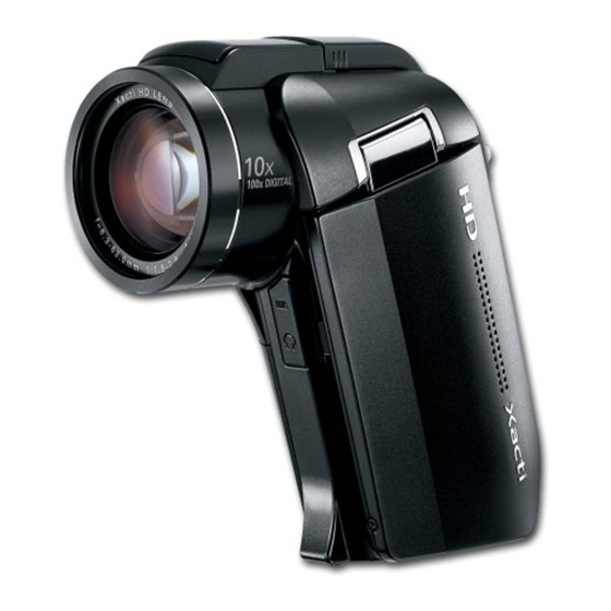
Sanyo VPC-HD1000 Service Manual
Digital movie camera
Hide thumbs
Also See for VPC-HD1000:
- Instruction manual (251 pages) ,
- Quick manual (33 pages) ,
- Instruction manual (243 pages)
Table of Contents
Advertisement
Quick Links
SERVICE MANUAL
Digital Movie Camera
Contents
1. OUTLINE OF CIRCUIT DESCRIPTION ............................... 3
2. DISASSEMBLY ................................................................... 11
3. ELECTRICAL ADJUSTMENT ............................................. 17
4. USB STORAGE INFORMATION REGISTRATION ............ 23
5. TROUBLESHOOTING GUIDE ............................................ 24
6. PARTS LIST ........................................................................ 26
RoHS
•This product does not contain any hazardous substances prohibited by the RoHS
Directive.
WARNING
•You are requested to use RoHS compliant parts for maintenance or repair.
•You are requested to use lead-free solder.
(This product has been manufactured using lead-free solder. Be sure to follow the
warning given on page 2 when carrying out repair work.)
CAUTION : Danger of explosion if battery is incorrectly replaced.
Replace only with the same or equivalent type recommended by the
manufacturer.
Discard used batteries according to the manufacturer's instructions.
NOTE : 1. Parts order must contain model number, part number, and description.
2. Substitute parts may be supplied as the service parts.
3. N. S. P. : Not available as service parts.
Design and specification are subject to change without notice.
SG211/U, EX, GX, U2, EX2, GX2 (R)
FILE NO.
VPC-HD1000
(Product Code : 168 110 01)
(U.S.A.) (Canada)
VPC-HD1000EX
(Product Code : 168 110 02)
(Europe) (U.K.) (South America)
(China) (Australia) (Hong Kong)
(Russia) (Middle East) (Africa)
(General) (Korea) (Taiwan)
VPC-HD1000GX
(Product Code : 168 110 03)
(South America) (China)
(Australia) (Hong Kong)
(General) (Korea) (Taiwan)
VPC-HD1000BK
(Product Code : 168 110 04)
(U.S.A.) (Canada)
VPC-HD1000EXBK
(Product Code : 168 110 05)
(Europe) (U.K.) (South America)
(China) (Australia) (Hong Kong)
(Russia) (Middle East) (Africa)
(General) (Korea) (Taiwan)
VPC-HD1000GXBK
(Product Code : 168 110 06)
(South America) (China)
(Australia) (Hong Kong)
(General) (Korea) (Taiwan)
REFERENCE No. SM5310715
Advertisement
Chapters
Table of Contents

Related Manuals for Sanyo VPC-HD1000


Summary of Contents for Sanyo VPC-HD1000
-
Page 1: Table Of Contents
FILE NO. SERVICE MANUAL VPC-HD1000 Digital Movie Camera (Product Code : 168 110 01) (U.S.A.) (Canada) VPC-HD1000EX (Product Code : 168 110 02) (Europe) (U.K.) (South America) (China) (Australia) (Hong Kong) (Russia) (Middle East) (Africa) (General) (Korea) (Taiwan) VPC-HD1000GX (Product Code : 168 110 03) - Page 2 PRODUCT SAFETY NOTICE The components designated by a symbol ( ! ) in this schematic diagram designates components whose value are of special significance to product safety. Should any component designated by a symbol need to be replaced, use only the part designated in the Parts List.
-
Page 3: Outline Of Circuit Description
1. OUTLINE OF CIRCUIT DESCRIPTION 1-1. CMOS CIRCUIT DESCRIPTION 1. IC Configuration The CMOS peripheral circuit block basically consists of the following ICs. IC901 (IMX017LQE-S) CMOS imager CDS, AGC, ADC built-in H driver, V driver, serial communication circuit built-in 2. IC901 (CMOS) [Structure] The electric charges which are generated when each pixel is optically converted are in turn converted into signal voltages... - Page 4 1-2. CP1 and VF1 CIRCUIT DESCRIPTION 1. Circuit Description 2. Outline of Operation 1-1. Digital clamp When the shutter opens, the reset signals (ASIC and CPU) The optical black section extracts averaged values from the and the serial signals (“take a picture” commands) from the 8- subsequent data to make the black level of the sensor output bit microprocessor are input and operation starts.
- Page 5 4. Lens drive block 5. Video Clip Recording and Playback 4-1. Focus drive 5-1. Recording The 16-bit serial data signals (LENS_SD) and (LENS_CK and The signal from the camera block is input to IC101 (ASIC). The LENS_EN) which are output from the ASIC (IC101) are used data that is input to the ASIC is input to SDRAM, and converts to drive (FOCUS A +, FOCUS A -, FOCUS B + and FOCUS B this data to encoded MPEG4 data, after which it is written in...
- Page 6 1-3. PWA POWER CIRCUIT DESCRIPTION 1. Outline 3. Motor System Power Output This is the main power circuit, and is comprised of the follow- BOOST 5 V and USB_5V are output. Feedback for the 5 V ing blocks. output is provided to the switching controller (Pin (36) of IC501) Switching controller (IC501) so that PWM control can be carried out.
- Page 7 1-4. ST1 STROBE CIRCUIT DESCRIPTION 1. Charging Circuit 2. Light Emission Circuit When UNREG power is supplied to the charge circuit and the When FLCLT signal is input from the ASIC, the stroboscope CHG signal from microprocessor becomes High (3.3 V), the emits light.
- Page 8 1-5. SYA CIRCUIT DESCRIPTION 1. Configuration and Functions For the overall configuration of the SYA block, refer to the block diagram. The SYA block centers around a 8-bit microprocessor (IC301), and controls camera system condition (mode). The 8-bit microprocessor handles the following functions. 1.
- Page 9 BAT_TMP Lithium battery temperature detection COMREQ Command request input Battery OFF detection signal input (L= OFF detection) BAT_OFF Serial communication request signal SREQ SCAN IN6 Keyscan input 6 IR_IN Infrared remote control signal input #RESET Reset input power monitoring XCIN Clock (32.768 kHz) XCOUT Clock (32.768 kHz)
- Page 10 4. Power Supply Control The 8-bit microprocessor controls the power supply for the overall system. The following is a description of how the power supply is turned on and off. When the battery is attached, a regulated 3.2 V voltage is normally input to the 8-bit microprocessor (IC301) by IC302, so that clock counting and key scanning is carried out even when the power switch is turned off, so that the camera can start up again.
-
Page 11: Disassembly
2. DISASSEMBLY 2-1. REMOVAL OF CABI LEFT, TB2 BOARD AND ST1 BOARD 1 2 3 4 5 6 7 8 1 2 3 4 5 6 7 8 15. Spacer TB2 1 2 3 4 5 6 7 8 1 2 3 4 5 6 7 8 1 2 3 4 5 6 7 8 17. - Page 12 2-2. REMOVAL OF LENS AND CP1 BOARD 1. Holder lens 10. Heat sink 19. FPC 2. Spacer AV jack 11. Earth heat sink 20. Screw 1.7 x 3 3. Two screws 1.7 x 3 12. Two FPCs 21. Top unit 4.
- Page 13 Assemble compl cabi front 4. Insert between plastic and sheet metal. 1. Attach the compl cabi front from the direction of above photo. 5. Push the main part. 2. Insert the bottom of cabi front, and 6. Close a gap certainly. turn in the direction of an arrow.
- Page 14 2-3. REMOVAL OF TB1 BOARD AND ST2 BOARD 1. Screw 1.7 x 2 2. Unit control 3. Spring shoe 4. Four screws 1.7 x 4.5 5. Holder shoe 6. Two screws 1.7 x 3 7. Holder base top 8. Button release 9.
- Page 15 2-4. REMOVAL OF TB3 BOARD, LCD AND VF1 BOARD 1. Cover mic 2. Spring cover card When assembling, 3. Dec right back tighten the screws order. a → b → c → d → e 4. Shaft cover SD 5. Cover card 6.
- Page 16 2-5. BOARD LOCATION ST2 board TB1 board ST1 board CP1 board VF1 board TB3 board TB2 board – 16 –...
-
Page 17: Electrical Adjustment
Download the calibration software and the firmware IBM R -compatible PC with pentium processor from the following URL. USB port http://www.digital-sanyo.com/overseas/service/ 40 MB RAM Place the DscCalDi.exe file, camapi32.dll file and Hard disk drive with at least 15 MB available QrCodeInfo.dll file together into a folder of your... - Page 18 3-6. The adjustment item which in necessary in part exchange CCD Black CCD White Lens Lens Point And Point Factory Adjust- Adjust- White Point Language storage Reset Defect Adjust- Cord Defect Detect Setting ment ment information Setting Detect Setting ment Adjustment registration (Infinity)
- Page 19 2. Lens Adjustment (1m) Dsc Calibration Copy Infinity calibration : AF_I_WIDE: 9 AF_I_MID1: 11 AF_I_MID2: 15 AF_I_MID3: 18 AF_I_MID4: 13 AF_I_MID5: 7 AF_I_MID6: -2 AF_I_TELE: -7 QR_Z_WIDE: -87 QR_F_I_WIDE: 111 Camera 0.5 cm (zoom wide) QR_F_I_TELE: -317 QR_Z_AORI: -87 Siemens QR_F_I_AORI: 111 star chart Preparation:...
- Page 20 3. AWB Adjustment DscCalDi Focus Result AF_TEMP_AD: 445 AF_WIDE: 9 AF_MID1: 11 AF_MID2: 15 AF_MID3: 25 AF_MID4: 26 AF_MID5: 24 AF_MID6: 19 AF_TELE: 17 Camera Adjustment value determination is effectuated using below val- Pattern box ues. The adjustment values fulfill the conditions below, they are de- termined as within specifications.
- Page 21 Adjustment value determination is effectuated using the "AGC", 4. CCD White Point Defect Detect Adjustment “CHECK", “CHECK_ND”, “IRIS_GAIN”, “IRIS_OFFSET”, "MS", Preparation: “MS_M”, “MS_C”, “MS_C2”, “MS_C3”, “IRIS_PWM1”, POWER switch: ON “IRIS_PWM2”, “IRIS_PWM3” and “IRIS_PWM4” values. If Adjustment method: AGC= a1 1. Double-click on the DscCalDi.exe. CHECK= wc0, wc1, wc2 2.
- Page 22 3-8. Factory Code Setting 3-12. Firmware uploading procedure 1. Check the "Factory Code" display within the Setting group. 1. Uploading the firmware should be carried out if the version 2. For U.S.A., Canada and NTSC general area number (COMPL PWB XX-X) on the replacement circuit If "FC_SANYO_U"...
-
Page 23: Usb Storage Information Registration
17.) 2. Double-click on the DscCalDi.exe. 3. Click on the Get button in the USB storage window and check the USB storage data. VID: SANYO PID: HD1000 Serial: Rev. : 1.00 4. -
Page 24: Troubleshooting Guide
5. TROUBLESHOOTING GUIDE POWER LOSS INOPERTIVE TAKING INOPERATIVE PUSH SHUTTER PUSH THE POWER BUTTON SW FOR A WHILE IC301-23, 24 IC301-44 CHECK S3003 (KEY_1st, KEY_2nd) CHECK SW UNIT (SCAN OUT2) LEVEL INPUT PULSE INPUT Q5007-2 (PON2) CHECK IC301, IC101, IC302-7 5.3 V IC501-26 (PON) CHECK IC501 PWA BLOCK... - Page 25 MEMO...
-
Page 26: Parts List
LOCATION PARTS NO. DESCRIPTION LOCATION PARTS NO. DESCRIPTION 7001 636 106 3791 CARTON INNER-SG211/EX, Note: Refer to the table of accessories. EXCEPT VPC-HD1000,VPC-HD1000BK 645 093 6753 ADAPTOR,DOCKING STATION 7001 636 106 3777 CARTON INNER-SG211/U, 645 093 6180 CABLE,DSC A/V-SG211 VPC-HD1000,VPC-HD1000BK... - Page 27 1.Table of accessories HDMI cable Microphone HDMI cable connection USB cable of hard cable disk...
- Page 28 SCR PAN PCS 1.7X3,VPC-HD1000BK, 636 105 1439 SPACER HOLDER JOINT-SG211 VPC-HD1000EXBK,VPC-HD1000GXBK 636 105 1026 COVER DC-SG211/J 411 177 9503 SCR S-TPG PAN PCS 1.7X3,VPC-HD1000, 636 105 2207 HOLDER LENS-SG211/J VPC-HD1000EX,VPC-HD1000GX 636 105 2764 COMPL PWB,TB-2 411 192 4200 SCR S-TPG PAN PCS 1.7X3.0,VPC-HD1000BK,...
- Page 29 CABINET AND CHASSIS PARTS 1 Cabinet 1 SG211/J PARTS LIST 1...
- Page 30 SPECIAL SCREW-1.7X3.0, VPC-HD1000, 636 105 5376 ASSY,WIRE TRIG IN-SG211(WHITE) VPC-HD1000EX,VPC-HD1000GX 636 105 2726 COMPL PWB,ST-2 411 184 6601 SCR PAN PCS 1.4X2.5,VPC-HD1000, 636 109 8359 SPACER FLASH B-SG211/J VPC-HD1000EX,VPC-HD1000GX 636 105 1071 COVER FLASH-SG211/J,VPC-HD1000, 411 213 3601 SCR PAN PCS 1.4X2.5,VPC-HD1000BK,...
- Page 31 CABINET AND CHASSIS PARTS 2 67(White) 66(Gray) Cabinet 2 SG211/J PARTS LIST 2...
- Page 32 ELECTRICAL PARTS Note: 1. Materials of Capacitors and Resistors are abbreviated as follows ; Resistors Capacitors MT-FILM Metallized Film Resistor MT-POLYEST Metallized Polyester Capacitor MT-GLAZE Metallized Glaze Resistor MT-COMPO Metallized Composite Capacitor OXIDE-MT Oxide Metallized Film Resistor TA-SOLID Tantalum Solid Capacitor AL-SOLID Aluminum Solid Capacitor NP-ELECT...
- Page 33 LOCATION PARTS NO. DESCRIPTION LOCATION PARTS NO. DESCRIPTION D5301 307 248 0701 DIODE MA21D3800 C1053 303 338 0309 CERAMIC 0.1U K 10V (CRYSTAL DEVICES) C1054 303 338 0309 CERAMIC 0.1U K 10V X1102 645 090 4400 OSC,CRYSTAL 48.00000MHZ C1055 303 338 0309 CERAMIC 0.1U K 10V X3001...
- Page 34 LOCATION PARTS NO. DESCRIPTION LOCATION PARTS NO. DESCRIPTION C5011 303 381 8109 CERAMIC 1U K 6.3V R1002 301 237 2905 MT-GLAZE 51 JA 1/16W C5013 303 338 0309 CERAMIC 0.1U K 10V R1003 301 105 7902 MT-GLAZE 0.000 ZA 1/16W C5017 303 381 8109 CERAMIC...
- Page 35 LOCATION PARTS NO. DESCRIPTION LOCATION PARTS NO. DESCRIPTION R3007 301 301 3500 MT-GLAZE 200 JA 1/16W R9555 301 226 1506 MT-GLAZE 0.000 ZA 1/16W R3008 301 224 9306 MT-GLAZE 1K JA 1/16W R9556 301 226 1506 MT-GLAZE 0.000 ZA 1/16W R3009 301 224 9306 MT-GLAZE...
- Page 36 LOCATI O N PARTS NO. DESCRI P TI O N LOCATI O N PARTS NO. DESCRI P TI O N COMPL PWB,VF-1 R5406 301 225 0708 MT-GLAZE 56K JA 1/16W 636 105 2702 R5407 301 224 9306 MT-GLAZE 1K JA 1/16W R5409 301 224 9009 MT-GLAZE...
-
Page 37: Circuit Diagrams & Printed Wiring Boards
CIRCUIT DIAGRAMS & PRINTED WIRING BOARDS TABLE OF CONTENTS OVERALL WIRING & BLOCK DIAGRAMS Page OVERALL WIRING ............................C3 OVERALL CIRCUIT ............................C4 POWER CIRCUIT ............................. C4 IMAGE SENSOR CIRCUIT ..........................C5 LENS CIRCUIT ..............................C5 MAIN CIRCUIT ..............................C6 SYSTEM CONTROL CIRCUIT ........................ - Page 38 NOTES: 1. All resistance values in "OHMS" unless otherwise noted. (K=1,000 ; M=1,000,000) µ 2. All capacitance values in " F" unless otherwise noted. µ p=pico farad ; ,u or U=micro farad µ 3. All inductance values in " H" unless otherwise noted. µ...
-
Page 39: Overall Wiring & Block Diagrams
OVERALL WIRING & BLOCK DIAGRAMS OVERALL WIRING CRADLE SW UNIT CN901 CN104 DGND DGND AFEDN5 AFEDN5 AFEDP5 AFEDP5 AFECKN AFECKN AFECKP AFECKP DGND DGND ADCK ADCK DGND DGND CCDEN CCDEN CCDCK CCDCK CCDSD CCDSD XCLR XCLR TGHD TGHD TGVD TGVD JW553 DGND DGND... -
Page 40: Overall Circuit
OVERALL CIRCUIT POWER CIRCUIT CHG_CNT LENS UNIT IC521 POWER_IN, DC_IN FLASH CHRG x10 F1.8 LTC4061EDD BATCHGER BAT+ PROG BATTERY CHARGE BATCHGI CN141 ST2 BOARD OUT5 L5011, Q5013 B_LEDAN OUT & CURRENT SD CARD STEPUP CN951 T5402 SOCKET DETECTOR B_LEDCA CA1 BOARD TRIGGER CIRCUIT TRANS... -
Page 41: Image Sensor Circuit
IMAGE SENSOR CIRCUIT LENS CIRCUIT LENS_TEMP (IC101 AK14pin) Z_SENSE IC101 A3.0V D1.8V I/F1.8V (IC101 AK15pin) EV2MA F_SENSE CN951 (IC101 AJ15pin) LENS_BLOCK SYSTEM ASIC IC951 BU2233GU LENS DRIVER B4, C8, D11, J4,J8 THERMISTOR G1, H1, D12, D13, G11, A7, B7, C7, C10, B7,A2 BOOST5V MVCC12,MVCC34... -
Page 42: Main Circuit
MAIN CIRCUIT D4CKOUT(48MHz) IC111 ADCK D4CKIN(74.17582MHz) CKOCK GENERATOR CCDEN/CCDSD/CCD TGHD/TGVD XCLR CN104 BOARD AFECKP/AFECKN(LVDS) AFEDP[0:11]/AFEDN[0:11](LVDS) X1102 IMAGE SENSOR 48.000MHz PAON1/PAON2/PAON3 PWA BLOCK SHUTTER+/ND ON/ND ON/ND OFF POWER SUPPLY LENS_SCLK/LENS_EN/LENS_SD IC951 LENS_MODE LENS DRIVER STATE1/STATE2 FPIOUT/ZPIOUT LENS CN951 UNIT IRISPWM IC971 IAMPPWM HALL OFFSET IRIS CONTROL... -
Page 43: System Control Circuit
SYSTEM CONTROL CIRCUIT STROBE CIRCUIT AL3.2V CHARGING CIRCUIT BOOST5V UNREGSY BACKUP3.2V XCIN C5401 T5401 D5402 VDD2 X3001 VDD3 4MHz POWER FILTER OSCILLATION CN541 RECTIFIER XCOUT 61 C5412 VDD1 TRANSFORMER CIRCUIT BLOCK UNREGST 20:22 Q3001 IC302 XCIN RESET IC301 BATTERY X3002 CHGSEL BACKUP 32.768KHz... -
Page 44: Circuit Diagrams
CIRCUIT DIAGRAMS CP1 BOARD (PWA) POWER 1AV4J11B8060N L5002 D5003 JK501 FBMH1608HL300 RB060M-30 MJC-040-D1-2 DC IN S_GND D_GND P_GND D5004 RB520S-30 P1-11000/SG211-J VOLTAGE: VIEW MODE, LCD ON I/F_GND A_GND L5003 D5005 USE BATTERY BAT+ BAT+ RB060M-30 FBMH1608HL300 F5006 DC JACK 2A32V IC504 L5001 D5006... -
Page 45: Ca1 Board Image Sensor
CA1 BOARD IMAGE SENSOR CCDCK XCLR TGVD C1-11000/SG211-J TGHD CCDSD VOLTAGE: VIEW MODE, LCD ON L9001 FBMH1608HL601 1608 L9002 FBMH1608HL601 1608 L9003 CN901 FBMH1608HM601 1608 DGND AFEDN5 AFEDN5 AFEDP5 AFEDP5 AFECKN AFECKN A_GND AFECKP AFECKP DGND ADCK DGND CCDEN C9002 CCDCK CCDSD XCLR... -
Page 46: Cp1 Board (Dma) Main
CP1 BOARD (DMA) MAIN D1-11000/SG211-J VOLTAGE: VIEW MODE, LCDON C1308 R1306 0;1/16Z D8 CLKIN R1033 1K;1/16J G2 LVDD CVDD VDD3 C1303 R1304 B6 VSS C1310 10K;1/16J 0.1;B C8 XO IC132 B8 XI TC7WH32FK DACK R1305 A8 BURNIN XDACK QTC7WH32FK--K 6.2K;1/16D DREQ A6 R1 IC131... - Page 47 CP1 BOARD (DMA) MAIN [UPPER-LEFT] D1-11000/SG211-J VOLTAGE: VIEW MODE, LCDON R1033 1K;1/16J A_VDD1.8 VDD1.0 VDD3 R1051 0;1/16Z VDD1.8 1608 AD18 AD17 AD16 AD15 AD14 AD13 AD12 AC13 R1052 0;1/16Z VDD_DDR1 VDD3 R24 VDD_DDR1 1608 T23 VDD_DDR1 A_VDD3 T24 VDD_DDR1 G14 VDD_DDR2 G15 VDD_DDR2 C1063 0.1;B...
- Page 48 CP1 BOARD (DMA) MAIN [UPPER-RIGHT] C1308 R1306 0;1/16Z D8 CLKIN R1033 1K;1/16J G2 LVDD CVDD VDD3 C1303 R1304 C1310 B6 VSS 10K;1/16J 0.1;B C8 XO IC132 B8 XI TC7WH32FK R1305 DACK QTC7WH32FK--K A8 BURNIN XDACK 6.2K;1/16D DREQ A6 R1 XDREQ IC131 B3 HVDD S1R72V17B00A20B...
- Page 49 CP1 BOARD (DMA) MAIN [LOWER-LEFT] TO SYA T15 GND T16 GND PAON1 PAON1 T17 GND QEV2MA------N PAON2 PAON2 T18 GND TO PWA PAON3 PAON3 U14 GND IR_IN IR_IN HOTLINE HOTLINE U15 GND IR_ON IR_ON COMREQ COMREQ U16 GND BOOST5V 16.0X16.0 ASIC_SDO ASIC_SDO U17 GND...
- Page 50 CP1 BOARD (DMA) MAIN [LOWER-RIGHT] DSCKEA R3 VSSQ DSCKBN DSCKBN DSCKBP DSCKBP MA------N DSCKAN DSCKAN DSCKAP DSCKAP ASIC_SDO ASIC_SDI 0X16.0 ASIC_SCK ZSREQ ZSREQ TEST0 AF26 R1009 L1007 TEST1 AF27 0;1/16Z FBMH1608HM102 CLOCK GEN EM ASIC AVSS12A_PLLS1 AF19 VDD1.8 IC111 1608 PL611S-26-777TCR AVSS12A_PLLS0 AF18...
-
Page 51: Cp1 Board (Dmb) Audio & Video
CP1 BOARD (DMB) AUDIO & VIDEO CN110 1AV4J11B8420G D2-11000/SG211-J HP_STBY HP_STBY HDMIINT HDMIINT G9 GND LVDSGND USB_D+ USB_D+ USB_D- K2 TC0 USB_D- TO DMA VBUS VBUS H2 NC ZAVJACK RCLK- RCLK- TO SYA ZAVJACK DOCK_PON RCLK+ RCLK+ TO DMA DOCK_PON H3 NC ZUSB_TRIG TO SYA... -
Page 52: Cp1 Board (Tca) Lens
CP1 BOARD (TCA) LENS F1-11000/SG211-J VDD3 CN951 1AV4J11VR290G HALL_IN+ HALL_IN+ VDD3 VDD3 HALL_OUT+ HALL_OUT+ HALL_IN- HALL_IN- BOOST5V HALL_OUT- HALL_OUT- TO PWA N.C.(GND) R9506 DRIVE+ 4.3;1/10F DRIVE+ R9507 DRIVE+ 4.3;1/10F DRIVE- DRIVE- G8 NC MVCC34 FOCUS_B+ DRIVE- F8 IN6A OUT4A E8 SI1 ZOOM_B+ D8 SO2 OUT2A... -
Page 53: Cp1 Board (Sya) System Control
CP1 BOARD (SYA) SYSTEM CONTROL AL3.2V AL3.2V SW3.2V BOOST5V BOOST5V BOOST5V UNREGSY UNREGSY TO PWA IR_IN Y1-11000/SG211-J ZSREQ TO DMA COMREQ VOLTAGE: VIEW MODE, LCD ON R3024 TO DMA,SYA BAT_T 47K;1/16J ZAVJACK ZUSB_TRIG TO DMB LCD0/Y0_ZBOOT TO DMA,DMB Q3004 UNR32AV00 R3019 10K;1/16J DC_IN1... -
Page 54: St2 Board Trigger Trans
ST2 BOARD TRIGGER TRANS ST1 BOARD STROBE Q3501 UP03396 S2-11000/SG211-J T5402 JW551 AWG32 JW553 AWG30 TTR-1026R-01 AWG30 JW547 IR_VCC TRG+ 2.0X1.25 BLUE S1-11000/SG211-J 2.0X1.25 WHITE 2.0X1.25 JW546 AWG32 VOLTAGE: STROBE AFTER CHARGE TO FLASH REFELECTOR IR_GND FLASH REFLECTOR BLACK 2.0X1.25 JW545 AWG32 IR_IN... -
Page 55: Tb1 Board Popup Sw
TB1 BOARD POPUP SW VF1 BOARD LCD CONNECTOR & MIC CN172 1AV4J11VQ060G LCD AN LCD AN T1-11000/SG211-J Z1-11000/SG211-J LCD CA S3501 ESE13V01C LCD CA JW351 AWG30 POPUP OUT 2.0X1.25 CN170 TO LCD POPUP 1AV4J11QP300G JW352 AWG30 POPUP IN LCD_AN LCD_CA 2.0X1.25 BLACK CL170... -
Page 56: Printed Wiring Boards (P.w.b.)
PRINTED WIRING BOARDS (P.W.B.) CP1 P.W.B. (SIDE A) -
Page 57: Cp1 P.w.b. (Side B)
CP1 P.W.B. (SIDE B) -
Page 58: Ca1 P.w.b. (Side A & B)
CA1 P.W.B. (SIDE A) CA1 P.W.B. (SIDE B) L9001 L9002 C9027 C9026 C9018 R9003 C9024 L9003... -
Page 59: St1 P.w.b. (Side A & B)
ST1 P.W.B. (SIDE A) ST1 P.W.B. (SIDE B) TB1 P.W.B. (SIDE A) TB1 P.W.B. (SIDE B) TB2 P.W.B. (SIDE A) TB2 P.W.B. (SIDE B) TB3 P.W.B. (SIDE A) TB3 P.W.B. (SIDE B) ST2 P.W.B. (SIDE A) ST2 P.W.B. (SIDE B) -
Page 60: Vf1 P.w.b. (Side A &B)
VF1 P.W.B. (SIDE A) VF1 P.W.B. (SIDE B) C1851 R1851 VA171 C1712... - Page 62 SANYO Electric Co., Ltd. Osaka, Japan Printed in Japan Sep./’07...