
Related Manuals for Motorola MVME162P2 Series


Summary of Contents for Motorola MVME162P2 Series
- Page 1 MVME162P2 VME Embedded Controller Installation and Use V162P2A/IH2 Edition of November 2000...
- Page 2 Printed in the United States of America. ® Motorola and the Motorola logo are registered trademarks of Motorola, Inc. MC68040™ and MC68060™ are trademarks of Motorola, Inc. IndustryPack™ and IP™ are trademarks of GreenSpring Computers, Inc. All other products mentioned in this document are trademarks or registered trademarks of...
- Page 3 The safety precautions listed below represent warnings of certain dangers of which Motorola is aware. You, as the user of the product, should follow these warnings and all other safety precautions necessary for the safe operation of the equipment in your operating environment.
- Page 4 Flammability All Motorola PWBs (printed wiring boards) are manufactured with a flammability rating of 94V-0 by UL-recognized manufacturers. EMI Caution This equipment generates, uses and can radiate electromagnetic energy. It may cause or be susceptible to electromagnetic interference (EMI) if not installed and used with adequate EMI protection.
- Page 5 While reasonable efforts have been made to assure the accuracy of this document, Motorola, Inc. assumes no liability resulting from any omissions in this document, or from the use of the information obtained therein. Motorola reserves the right to revise this document and to make changes from time to time in the content hereof without obligation of Motorola to notify any person of such revision or changes.
- Page 6 If the documentation contained herein is supplied, directly or indirectly, to the U.S. Government, the following notice shall apply unless otherwise agreed to in writing by Motorola, Inc. Use, duplication, or disclosure by the Government is subject to restrictions as set forth in subparagraph (b)(3) of the Rights in Technical Data clause at DFARS 252.227-7013 (Nov.
-
Page 7: Table Of Contents
Contents About This Manual Summary of Changes ....................xvi Overview of Contents ....................xvi Comments and Suggestions ..................xvii Conventions Used in This Manual................xviii CHAPTER 1 Hardware Preparation and Installation Introduction........................1-1 Getting Started ......................1-1 Overview of Installation Procedure ..............1-1 Equipment Required ...................1-2 Guidelines for Unpacking ...................1-3 ESD Precautions ....................1-3 Preparing the Board ....................1-4 MVME162P2 Configuration ................1-5... - Page 8 CHAPTER 2 Startup and Operation Introduction ....................... 2-1 Front Panel Switches and Indicators ..............2-1 Initial Conditions ....................... 2-2 Applying Power ......................2-3 Pre-Startup Checklist....................2-4 Bringing up the Board ....................2-5 Autoboot ......................2-9 ROMboot......................2-10 Network Boot ....................2-11 Restarting the System ....................
- Page 9 Microprocessor ....................4-6 MC68xx040 Cache ..................4-6 No-VMEbus-Interface Option ................4-7 Memory Options ....................4-7 DRAM ......................4-7 SRAM......................4-8 About the Battery..................4-9 EPROM and Flash Memory ..............4-11 Battery-Backed-Up RAM and Clock..............4-12 VMEbus Interface and VMEchip2 ..............4-12 I/O Interfaces ....................4-12 Serial Communications Interface ..............4-13 IndustryPack (IP) Interfaces ..............4-13 Ethernet Interface ..................4-14 SCSI Interface....................4-15 SCSI Termination ..................4-15...
- Page 10 APPENDIX B Troubleshooting Solving Startup Problems ..................B-1 APPENDIX C Network Controller Data Network Controller Modules Supported ..............C-1 APPENDIX D Disk/Tape Controller Data Controller Modules Supported ................. D-1 Default Configurations ..................... D-2 IOT Command Parameters ..................D-5 APPENDIX E Related Documentation MCG Documents .......................E-1 Manufacturers’...
- Page 11 List of Figures Figure 1-1. MVME162P2 Board Layout ..............1-6 Figure 2-1. MVME162P2/Firmware System Startup ..........2-3 Figure 4-1. MVME162P2 Block Diagram..............4-5...
- Page 13 Table 5-7. VMEbus Connector P2 Pin Assignment...........5-8 Table A-1. MVME162P2 Specifications ..............A-1 Table B-1. Troubleshooting MVME162P2 Boards ..........B-1 Table E-1. Motorola Computer Group Documents ..........E-1 Table E-2. Manufacturers’ Documents ..............E-2 Table E-3. Related Specifications ................E-3 xiii...
- Page 15 About This Manual MVME162P2 VME Embedded Controller Installation and Use provides instructions for hardware preparation and installation; a board-level hardware overview; and firmware-related general information and startup instructions for the MVME162P-242 series of embedded controllers, known collectively as the ‘‘MVME162P2’’ because they are equipped with the “Petra”...
-
Page 16: Summary Of Changes
Summary of Changes This is the second edition of MVME162P2 Installation and Use. It supersedes the June 2000 edition and incorporates the following updates. Date Description of Change October 2000 In the description of the snoop control switch on page 1-18, entries in the table concerning boards equipped with the MC68060 processor have been corrected. -
Page 17: Comments And Suggestions
Documentation, provides all documentation related to the MVME162P2. Comments and Suggestions Motorola welcomes and appreciates your comments on its documentation. We want to know what you think about our manuals and how we can make them better. Mail comments to:... -
Page 18: Conventions Used In This Manual
Conventions Used in This Manual The following typographical conventions are used in this document: bold is used for user input that you type just as it appears; it is also used for commands, options and arguments to commands, and names of programs, directories and files. -
Page 19: Introduction
1Hardware Preparation and Installation Introduction This chapter provides unpacking instructions, hardware preparation guidelines, and installation instructions for the MVME162P2 VME Embedded Controller. Getting Started This section supplies an overview of startup procedures applicable to the MVME162P2. Equipment requirements, directions for unpacking, and ESD precautions that you should take complete the section. -
Page 20: Equipment Required
Hardware Preparation and Installation Table 1-1. Startup Overview (Continued) What you need to do... Refer to... Connect any other equipment you Connector Pin Assignments in Chapter 5. will be using. For more information on optional devices and equipment, refer to the documentation provided with the equipment. Power up the system. -
Page 21: Guidelines For Unpacking
MVME162P2 board. Use ESD Motorola strongly recommends the use of an antistatic wrist strap and a conductive foam pad when you install or upgrade the board. Electronic components can be extremely sensitive to ESD. After removing the board... -
Page 22: Preparing The Board
Hardware Preparation and Installation Turn the system’s power off before you perform these procedures. Failure to turn the power off before opening the enclosure can result in personal injury or damage to the equipment. Hazardous voltage, current, and energy Warning levels are present in the chassis. -
Page 23: Mvme162P2 Configuration
IP Reset Mode (S5 Pin 3) on page 1-19 Flash Write Enable Mode (S5 Pin 4) on page 1-20 On-Off-On MCECC DRAM Size (S6) on page 1-21 J15 (also J24, if present) is a PLD programming header for lab or factory use. It has no user function. http://www.motorola.com/computer/literature... -
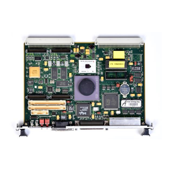
Page 24: Figure 1-1. Mvme162P2 Board Layout
Hardware Preparation and Installation MVME162 FAIL RUN SCON FUSES ABORT RESET Figure 1-1. MVME162P2 Board Layout Computer Group Literature Center Web Site... -
Page 25: Vme System Controller (J1)
Other IP interfaces require that the strobe be disconnected. With a jumper installed between J11 pins 1-2, a programmable frequency source is connected to the Strobe∗ signal on the IP bus (for details, refer to the Petra/IP2 chip programming model in the Programmer’s Reference Guide). http://www.motorola.com/computer/literature... -
Page 26: Scsi Termination (J12)
Hardware Preparation and Installation If the jumper is removed from J11, the strobe line is available for a sideband type of messaging between IP modules. The Strobe∗ signal is not connected to any active devices on the board, but it may be connected to a pull-up resistor. -
Page 27: Ip Bus Clock (J13)
(0) for 8MHz, or set (1) to match the processor bus clock speed. Caution If the jumper and the CSR bit are not configured the same, the board may not run properly. Bus Clock = 8MHz Bus Clock = Processor Bus Clock (Factory configuration) (from MPU Bus Clock) http://www.motorola.com/computer/literature... -
Page 28: Sram Backup Power Source (J14)
Hardware Preparation and Installation SRAM Backup Power Source (J14) Header J14 determines the source for onboard static RAM backup power. The MVME162P2 is factory-configured to use VMEbus +5V standby voltage as a backup power source for the SRAM (i.e., jumpers are installed across pins 1-3 and 2-4). -
Page 29: Flash Write Protection (J16)
(128 Kbit x 8; 256 Kbit x 8; 512 Kbit x 8 — the default configuration; 1 Mbit x 8) and also permit disabling of the Flash memory. Header J20 provides eight jumper locations to configure the EPROM sockets. http://www.motorola.com/computer/literature 1-11... - Page 30 Hardware Preparation and Installation CONFIGURATION 3: 512K x 8 EPROMs CONFIGURATION 1: 128K x 8 EPROMs (FACTORY DEFAULT) CONFIGURATION 2: 256K x 8 EPROMs CONFIGURATION 4: 1M x 8 EPROMs CONFIGURATION 5: 1M x 8 EPROMs ONBOARD FLASH DISABLED 1-12 Computer Group Literature Center Web Site...
-
Page 31: Table 1-3. Eprom/Flash Mapping - 128K X 8 Eproms
$FF800000 - $FF83FFFF EPROM A (XU1) Set to OFF $FF840000 - $FF87FFFF EPROM B (XU2) $FFA00000 - $FFBFFFFF Onboard Flash $FF800000 - $FF9FFFFF Onboard Flash Set to ON $FFA00000 - $FFA3FFFF EPROM A (XU1) $FFA40000 - $FFA7FFFF EPROM B (XU2) http://www.motorola.com/computer/literature 1-13... -
Page 32: Table 1-5. Eprom/Flash Mapping - 512K X 8 Eproms
Hardware Preparation and Installation Table 1-5. EPROM/Flash Mapping — 512K x 8 EPROMs GPI3 Address Range Device Accessed $FF800000 - $FF87FFFF EPROM A (XU1) Set to OFF $FF880000 - $FF8FFFFF EPROM B (XU2) $FFA00000 - $FFBFFFFF Onboard Flash $FF800000 - $FF9FFFFF Onboard Flash Set to ON $FFA00000 - $FFA7FFFF... -
Page 33: Mc2 Dram Size (S3)
S3 comes into play in the MC2 memory controller model. S3 is a four- segment slide switch whose lower three segments establish the size of the parity DRAM (segment 4 is not used.) Refer to the illustration and table below for specifics. MC2 DRAM SIZE 16MB (factory configuration) 2734 0004 http://www.motorola.com/computer/literature 1-15... -
Page 34: General-Purpose Readable Switch (S4 Pin 5)
Hardware Preparation and Installation Table 1-8. MC2 DRAM Size Settings MC2 DRAM Segment 1 Segment 2 Segment 3 Size Disabled 16MB Notes As shown in the table, the Petra/MC2 interface supports parity DRAM emulations up to 16MB. For sizes beyond 16MB, it is necesary to use the MCECC memory model. - Page 35 ON=FLASH; OFF=EPROM ON=FLASH; OFF=EPROM GPI3 REFER TO DEBUG MANUAL REFER TO DEBUG MANUAL GPI2 REFER TO DEBUG MANUAL REFER TO DEBUG MANUAL GPI1 GPI0 REFER TO DEBUG MANUAL REFER TO DEBUG MANUAL Flash Selected (factory configuration) 2735 0004 http://www.motorola.com/computer/literature 1-17...
-
Page 36: Ip Dma Snoop Control (S5 Pins 1/2)
Hardware Preparation and Installation IP DMA Snoop Control (S5 Pins 1/2) Segments 1 and 2 of switch S5 define the state of the snoop control bus when an IP DMA controller is local bus master. As shown in Table 1-9, S5 segment 1 controls Snoop Control signal 1 on the MC680x0 processor. -
Page 37: Ip Reset Mode (S5 Pin 3)
In IP1 mode, the IP reset control bit clears itself after after a 1msec interval. IP resets may occur in response to a software write, a power-up reset, or a local bus reset. For details, refer to the Programmer’s Reference Guide listed under “Related Documentation” in Appendix E. http://www.motorola.com/computer/literature 1-19... -
Page 38: Flash Write Enable Mode (S5 Pin 4)
Hardware Preparation and Installation Flash Write Enable Mode (S5 Pin 4) Segment 4 of switch S5 defines the Flash memory controller model (MC1 or MC2) to be emulated when enabling or disabling Flash memory accesses on the MVME162P2 board. With S5 segment 4 set to (the factory configuration), the board initializes in MC2 mode. -
Page 39: Mcecc Dram Size (S6)
S6 comes into play in the MCECC memory controller model. S6 is a four- segment slide switch whose lower three segments establish the size of the ECC DRAM (segment 4 is not used.) Refer to the illustration and table below for specifics. 16MB MCECC DRAM (factory configuration ) 2737 0004 http://www.motorola.com/computer/literature 1-21... -
Page 40: Installation Instructions
Hardware Preparation and Installation Table 1-10. MCECC DRAM Size Settings MCECC Segment 1 Segment 2 Segment 3 DRAM Size 16MB 32MB 64MB Notes For the MCECC memory model to be enabled, the MC2 emulation must be disabled. You disable the MC2 memory model by setting the MC2 DRAM size select switch (S3) to 110 (Off/Off/On). -
Page 41: Ip Installation On The Mvme162P2
– Connect user-supplied 50-pin cables to J3 and J4 as needed. (Because of the varying requirements for each different kind of IP, Motorola does not supply these cables.) – Bring the IP cables out the narrow slots in the MVME162P2 front panel and attach them to the appropriate external equipment, depending on the nature of the particular IP(s). - Page 42 BUS GRANT slot occupied by the MVME162P2. Note Some VME backplanes (e.g., those used in Motorola "Modular Chassis" systems) have an autojumpering feature for automatic propagation of the IACK and BG signals. Step 6 does not apply to such backplane designs.
-
Page 43: System Considerations
Installation Instructions – Note that some cables are not provided with the MVME162P2 and must be made or purchased by the user. (Motorola recommends shielded cable for all peripheral connections to minimize radiation.) 8. Connect the peripheral(s) to the cable(s). - Page 44 Hardware Preparation and Installation situation in which the system might lack this global bus timeout: when the MVME162P2 is not the system controller and there is no global bus timeout elsewhere in the system. Multiple MVME162P2s may be installed in a single VME chassis. In general, hardware multiprocessor features are supported.
-
Page 45: Serial Connections
Chapter 5, Pin Assignments. For additional information on the MVME162P2 serial communications interface, refer to the Z85230 Serial Communications Controller Product Brief listed under Manufacturer’s Documents in Appendix E, Related Documentation. For additional information on the EIA-232-D interface, refer to the EIA-232-D Standard. http://www.motorola.com/computer/literature 1-27... - Page 46 Hardware Preparation and Installation 1-28 Computer Group Literature Center Web Site...
-
Page 47: Introduction
2Startup and Operation Introduction This chapter provides information on powering up the MVME162P2 VME Embedded Controller after its installation in a system, and describes the functionality of the switches, status indicators, and I/O ports. For programming information, consult the MVME1X2P2 VME Embedded Controller Programmer’s Reference Guide. -
Page 48: Initial Conditions
Startup and Operation Table 2-1. MVME162P2 Front Panel Controls Control/Indicator Function LED (DS1, red) Board failure. Lights if a fault occurs on the MVME162P2 board. FAIL LED (DS2, green) CPU activity. Indicates that one of the local bus masters is executing a local bus cycle. -
Page 49: Applying Power
Power-up/reset initialization STARTUP Initialization of devices on the MVME162P2 INITIALIZATION module/system Power-On Self-Test diagnostics POST Firmware-configured boot mechanism, BOOTING if so configured. Default is no boot. Interactive, command-driven on-line MONITOR debugger, when terminal connected. Figure 2-1. MVME162P2/Firmware System Startup http://www.motorola.com/computer/literature... -
Page 50: Pre-Startup Checklist
Startup and Operation Pre-Startup Checklist Before you power up the MVME162P2 system, be sure that the following conditions exist: 1. Jumpers and/or configuration switches on the MVME162P2 VME Embedded Controller and associated equipment are set as required for your particular application. 2. -
Page 51: Bringing Up The Board
3. Header J11 enables or disables the IP bus strobe function on the MVME162P2. The factory configuration puts no jumper on J11, disabling the Strobe∗ signal to the Petra/IP2 chip. Verify that this setting is appropriate for your application. http://www.motorola.com/computer/literature... -
Page 52: Table 2-2. Software-Readable Switches
Startup and Operation Table 2-2. Software-Readable Switches Bit No. S4 Segment Function GPI0 When set to 1 (high), instructs the debugger to use local static RAM for its work page (variables, stack, vector tables, etc.). GPI1 When set to 1 (high), instructs the debugger to use the default setup/operation parameters in ROM instead of the user setup/operation parameters in NVRAM. - Page 53 12. If you have equipment (such as a host computer system and/or a serial printer) to connect to the other EIA-232-D port connectors, connect the appropriate cables and configure the port(s) as detailed http://www.motorola.com/computer/literature...
- Page 54 Startup and Operation in Step above. After power-up, you can reconfigure the port(s) by programming the MVME162P2 Z85230 Serial Communications Controllers (SCCs) or by using the 162Bug PF command. 13. Power up the system. 162Bug executes some self-checks and displays the debugger prompt if the firmware is in Board 162-Bug>...
-
Page 55: Autoboot
The Autoboot process is controlled by parameters contained in the ENV command. These parameters allow the selection of specific boot devices and files, and allow programming of the Boot delay. Refer to the ENV command description in Chapter 3 for more details. http://www.motorola.com/computer/literature... -
Page 56: Romboot
XU2. This leaves the remaining EPROM socket (XU1) and the Flash memory available for your use. Note You may wish to contact your Motorola sales office for assistance in using these resources. The ROMboot function is configured/enabled via the ENV command (refer to Chapter 3) and is executed at power-up (optionally also at reset). -
Page 57: Network Boot
For complete details on using the ROMboot function, refer to the Debugging Package for Motorola 68K CISC CPUs User’s Manual. Network Boot Network Auto Boot is a software routine in the 162Bug Flash/EPROM which provides a mechanism for booting an operating system using a network (local Ethernet interface) as the boot device. -
Page 58: Restarting The System
Startup and Operation Network Auto Boot is controlled by parameters contained in the NIOT and ENV commands. These parameters allow the selection of specific boot devices, systems, and files, and allow programming of the Boot delay. Refer to the ENV command description in Chapter 3 for more details. Restarting the System You can initialize the system to a known state in three different ways: Reset, Abort, and Break. -
Page 59: Abort
A break removes any breakpoints in your code and keeps the breakpoint table intact. If the function was entered using SYSCALL, Break also takes a snapshot of the machine state. This machine state is then accessible to you for diagnostic purposes. http://www.motorola.com/computer/literature 2-13... -
Page 60: Diagnostic Facilities
Refer to the Debugging Package 162-Diag> for Motorola 68K CISC CPUs User’s Manual for complete descriptions of the diagnostic routines available and instructions on how to invoke them. Note that some diagnostics depend on restart defaults that are set up only in a particular restart mode. -
Page 61: Introduction
A list of 162Bug commands appears at the end of the chapter. For complete user information about 162Bug, refer to the Debugging Package for Motorola 68K CISC CPUs User’s Manual and to the MVME162Bug Diagnostics User’s Manual, listed under Related Documentation. - Page 62 162Bug Firmware 162Bug includes: Commands for display and modification of memory Breakpoint and tracing capabilities A powerful assembler/disassembler useful for patching programs A “self-test at power-up” feature which verifies the integrity of the system In addition, the TRAP #15 system calls make various 162Bug routines that handle I/O, data conversion, and string functions available to user programs.
-
Page 63: 162Bug Implementation
162Bug Implementation If you have used one or more of Motorola’s other debugging packages, you will find the CISC 162Bug very similar. Some effort has also been made to improve the consistency of interactive commands. For example, delimiters between commands and arguments may be commas or spaces interchangeably. -
Page 64: Memory Requirements
162Bug Firmware Memory Requirements The program portion of 162Bug is approximately 512KB of code, consisting of download, debugger, and diagnostic packages and contained entirely in Flash memory or EPROM. The 162Bug firmware executes from address $FF800000 whether in Flash or EPROM. If you set switch S4 segment 5 to , the address spaces of the Flash and EPROM are swapped. -
Page 65: Using 162Bug
This allows you to correct entry errors, if necessary, with the control characters described in the Debugging Package for Motorola 68K CISC CPUs User’s Manual, Chapter 1. After the debugger executes the command you have entered, the prompt reappears. -
Page 66: Debugger Commands
Debugger Commands The 162Bug debugger commands are summarized in the following table. The commands are described in detail in the Debugging Package for Motorola 68K CISC CPUs User’s Manual. Table 3-2. Debugger Commands Command Description Automatic Bootstrap Operating System... - Page 67 Memory Set Memory Write Automatic Network Boot Operating System Network Boot Operating System and Halt Network Boot Operating System NIOC Network I/O Control NIOP Network I/O Physical NIOT Network I/O Teach NPING Network Ping Offset Registers Display/Modify Printer Attach http://www.motorola.com/computer/literature...
-
Page 68: Modifying The Environment
162Bug Firmware Table 3-2. Debugger Commands (Continued) Command Description NOPA Printer Detach Port Format NOPF Port Detach PFLASH Program FLASH Memory Put RTC Into Power Save Mode for Storage ROMboot Enable NORB ROMboot Disable Register Display REMOTE Connect the Remote Modem to CSO RESET Cold/Warm Reset Read Loop... -
Page 69: Cnfg - Configure Board Information Block
NVRAM. The CNFG and ENV commands are both described in the Debugging Package for Motorola 68K CISC CPUs User’s Manual, listed in Appendix E, Related Documentation. Refer to that manual for general information about their use and capabilities. - Page 70 Refer to the MVME1X2P2 VME Embedded Controller Programmer’s Reference Guide for the actual location and other information about the Board Information Block. Refer to the Debugging Package for Motorola 68K CISC CPUs User's Manual for a CNFG description and examples.
-
Page 71: Env - Set Environment
Use the ENV command to view and/or configure interactively all 162Bug operational parameters that are kept in Non-Volatile RAM (NVRAM). Refer to the Debugging Package for Motorola 68K CISC CPUs User’s Manual for a description of the use of ENV. Additional information on registers in the MVME162P2 that affect these parameters appears in your MVME1X2P2 VME Embedded Controller Programmer’s Reference... - Page 72 162Bug Firmware Table 3-3. ENV Command Parameters (Continued) ENV Parameter and Options Default Meaning of Default Negate VMEbus SYSFAIL∗ Negate VMEbus SYSFAIL∗ after successful Always [Y/N] completion or entrance into the bug command monitor. Local SCSI Bus Reset on No local SCSI bus reset on debugger startup. Debugger Startup [Y/N] Local SCSI Bus Negotiations Asynchronous negotiations.
- Page 73 This must be a multiple of the debugger work page, modulo $10000 (64KB). In a multi-controller environment, each MVME162P2 board could be set to start its work page at a unique address to allow multiple debuggers to operate simultaneously. http://www.motorola.com/computer/literature 3-13...
- Page 74 162Bug Firmware Table 3-3. ENV Command Parameters (Continued) ENV Parameter and Options Default Meaning of Default Memory Search Ending Address 00100000 Top limit of the Bug’s search for a work page. If no 64KB contiguous block of memory is found in the range specified by Memory Search Starting Address and Memory Search Ending Address parameters, the bug will place its work page in the onboard static RAM on the...
- Page 75 If only 2MB SRAM is present, it defaults to address 00000000. Size of Static Memory 00080000 The size of the SRAM type memory present. The default is the calculated size of the onboard SRAM or an SRAM type mezzanine. http://www.motorola.com/computer/literature 3-15...
- Page 76 162Bug Firmware Table 3-3. ENV Command Parameters (Continued) ENV Parameter and Options Default Meaning of Default ENV asks the following series of questions to set up the VMEbus interface for the MVME162 series modules. You should have a working knowledge of the VMEchip2 as given in the MVME1X2P2 VME Embedded Controller Programmer’s Reference Guide in order to perform this configuration.
- Page 77 Decoder #3. This is the default if the board size of local contains less than 16MB of calculated RAM. Do not set up and enable the Master Address Decoder #3. This is the default for boards containing at least 16MB of calculated RAM. http://www.motorola.com/computer/literature 3-17...
- Page 78 162Bug Firmware Table 3-3. ENV Command Parameters (Continued) ENV Parameter and Options Default Meaning of Default Master Starting Address #3 00000000 Base address of the VMEbus resource that is accessible from the local bus. If enabled, the value is calculated as one more than the calculated size of memory.
-
Page 79: Configuring The Industrypacks
IndustryPack modules (IPs) on MVME162P2s. The MVME1X2P2 VME Embedded Controller Programmer’s Reference Guide describes the base addresses and the IP register settings. Refer to that manual for information on setting base addresses and register bits. http://www.motorola.com/computer/literature 3-19... - Page 80 162Bug Firmware IP A Base Address = 00000000? IP B Base Address = 00000000? IP C Base Address = 00000000? IP D Base Address = 00000000? Base address for mapping IP modules. Only the upper 16 bits are significant. IP D/C/B/A Memory Size = 00000000? Define the memory size requirements for the IP modules: Bits...
- Page 81 VMEbus F Pages (A24/A32) $FFFF0000 $FFFFFFFF Master VMEbus Short I/O (A16) $FF800000 $FFBFFFFF Master Flash/PROM $FFF00000 $FFFEFFFF Master Local I/O $00000000 $00000000 Master Industry Pack A $00000000 $00000000 Master Industry Pack B $00000000 $00000000 Master Industry Pack C http://www.motorola.com/computer/literature 3-21...
- Page 82 162Bug Firmware $00000000 $00000000 Master Industry Pack D $00000000 $00000000 Slave VMEbus Slave #1 $00000000 $00000000 Slave VMEbus Slave #2 3-22 Computer Group Literature Center Web Site...
-
Page 83: Chapter 4 Functional Description
4Functional Description Introduction This chapter describes the MVME162P2 VME embedded controller on a block diagram level. The Summary of Features provides an overview of the MVME162P2, followed by a detailed description of several blocks of circuitry. Figure 4-1 shows a block diagram of the overall board architecture. - Page 84 Functional Description Table 4-1. MVME162P2 Features (Continued) Feature Description Switches switches on front panel RESET ABORT Four: Board Fail (FAIL) , CPU Activity (RUN) , System Controller ( SCON Status LEDs Fuse Status ( FUSES Four 32-bit tick timers and watchdog timer in Petra ASIC Timers Two 32-bit tick timers and watchdog timer in VMEchip2 ASIC Interrupts...
-
Page 85: Processor And Memory
RJ45 connectors on the front panel. In addition, the panel has cutouts for routing of flat cables to the optional IndustryPack modules. SCSI devices are interfaced via an industry-standard 68-pin panel connector. The Ethernet interface uses a DB15 connector. http://www.motorola.com/computer/literature... -
Page 86: Asics
Functional Description ASICs The following ASICs are used on the MVME162P2: VMEchip2 ASIC (VMEbus interface). Provides two tick timers, a watchdog timer, programmable map decoders for the master and slave interfaces, and a VMEbus-to/from-local-bus DMA controller as well as a VMEbus-to/from-local-bus non-DMA programmed access interface, a VMEbus interrupter, a VMEbus system controller, a VMEbus interrupt handler, and a VMEbus requester. -
Page 87: Figure 4-1. Mvme162P2 Block Diagram
Block Diagram Figure 4-1. MVME162P2 Block Diagram http://www.motorola.com/computer/literature... -
Page 88: Functional Description
Functional Description Functional Description This section contains a functional description of the major blocks on the MVME162P2. Data Bus Structure The local bus on the MVME162P2 is a 32-bit synchronous bus that is based on the MC68040 bus, and which supports burst transfers and snooping. -
Page 89: No-Vmebus-Interface Option
(SDRAM). Depending on build options chosen at the time of manufacture, various versions of the MVME162P2 have the SDRAM configured to model 1MB, 4MB, 8MB, or 16MB of parity-protected DRAM or 4MB, 8MB, 16MB, or 32MB of ECC-protected DRAM. http://www.motorola.com/computer/literature... -
Page 90: Sram
Functional Description The SDRAM memory array itself is always a single-bit error correcting and multi-bit error detection memory, irrespective of which interface model you use to access the SDRAM. When the MC2 (parity) memory controller interface is used to access the SDRAM, single-bit errors are undetectable to users and multi-bit errors are defined to be parity errors. -
Page 91: About The Battery
40° C. If the power-on duty cycle is 50% (the board is powered on half of the time), the battery lifetime is four years. At lower ambient temperatures, the backup time is correspondingly longer. http://www.motorola.com/computer/literature... - Page 92 Functional Description If you intend to place the board in storage, putting the M48T58 in power- save mode by stopping the oscillator will prolong battery life. This is especially important at high ambient temperatures. To enter power-saving mode, execute the 162Bug PS command (refer to Debugger Commands in Chapter 3) or its equivalent application-specific command.
-
Page 93: Eprom And Flash Memory
Flash memory blank (the factory uses the VMEbus to program the Flash memory with debugger code). To use the debugger firmware, be sure that configuration switch S4 is set for the EPROM memory map. Refer to chapters 1 and 3 for further details. http://www.motorola.com/computer/literature 4-11... -
Page 94: Battery-Backed-Up Ram And Clock
Functional Description Battery-Backed-Up RAM and Clock An M48T58 RAM and clock chip is used on the MVME162P2. This chip provides a time-of-day clock, oscillator, crystal, power fail detection, memory write protection, 8KB of RAM, and a battery in one 28-pin package. -
Page 95: Serial Communications Interface
Refer to the IP2 Programming Model in the MVME1X2P2 VME Embedded Controller Programmer's Reference Guide for details of the IP interface. Refer to Chapter 5, Pin Assignments for the pin assignments of the IP connectors. http://www.motorola.com/computer/literature 4-13... -
Page 96: Ethernet Interface
Functional Description Notes MVME162P2 boards do not monitor power supply +5 Vdc power and assert IP reset if the power falls too low. Instead, IP reset is handled by the ENV command of the 162Bug debugger, as described in Chapter 3. The IP reset is also driven active by the power-up reset signal. -
Page 97: Scsi Interface
SCSI bus can provide power to the TERM power line, the FUSES LED does not directly indicate the condition of the fuse. Local Resources The MVME162P2 includes many resources for the local processor. These include tick timers, software-programmable hardware interrupts, a watchdog timer, and a local bus timeout. http://www.motorola.com/computer/literature 4-15... -
Page 98: Programmable Tick Timers
Functional Description Programmable Tick Timers Six 32-bit programmable tick timers with 1µs resolution are available: two in the VMEchip2 ASIC and four in the Petra/MC2 chip. The tick timers may be programmed to generate periodic interrupts to the processor. Refer to the VMEchip2 and Petra/MC2 descriptions in the MVME1X2P2 VME Embedded Controller Programmer’s Reference Guide for detailed programming information. -
Page 99: Local Bus Arbiter
"No VMEbus Interface" option). Local Bus Arbiter The local bus arbiter implements a fixed priority (see Table 4-2). Table 4-2. Local Bus Arbitration Priority Device Priority Note Highest Industry Pack DMA SCSI VMEbus Next Lowest MC680x0/MC68LC0x0 Lowest http://www.motorola.com/computer/literature 4-17... -
Page 100: Connectors
Functional Description Connectors The MVME162P2 has two 96-position DIN connectors: P1 and P2. P1 rows A, B, C, and P2 row B provide the VMEbus interconnection. P2 rows A and C are not used. The serial ports on the MVME162P2 are connected to four 8-pin RJ45 female connectors ( J17) on the front panel. -
Page 101: Connector Pin Assignments
Table 5-5 VMEbus connector P1 Table 5-6 VMEbus connector P2 Table 5-7 The tables in this chapter furnish pin assignments only. For detailed descriptions of the interconnect signals, consult the support information for the MVME162P2 (available through your Motorola sales office). -
Page 102: Remote Reset Connector - J2
Pin Assignments Remote Reset Connector - J2 The MVME162P2 has a 20-pin connector (J2) mounted behind the front panel. When the MVME162P2 board is enclosed in a chassis and the front panel is not visible, this connector enables you to extend the reset, abort and LED functions to the control panel of the system, where they remain accessible. -
Page 103: Table 5-2. Industrypack Interconnect Signals
IPD5 IPD6 IPD7 IPD8 IPD9 IPD10 IPD11 IPD12 IPD13 IPD14 IPD15 BS0∗ BS1∗ –12V +12V R/W∗ IDSEL∗ DMAREQ0∗ MEMSEL∗ DMAREQ1∗ INTSEL∗ DMACK∗ IOSEL∗ No Connection IPA1 DMAEND∗ IPA2 ERROR∗ IPA3 INT_REQ0∗ IPA4 INT_REQ1∗ IPA5 STROBE∗ IPA6 ACK∗ No Connection http://www.motorola.com/computer/literature... -
Page 104: Ethernet Connector - J9
Pin Assignments Ethernet Connector - J9 The MVME162P2’s Ethernet interface is implemented with a DB15 connector located on the front panel of the board. The pin assignments for this connector are listed in the following table. Table 5-3. DB15 Ethernet Connector Pin Assignments No Connection C–... -
Page 105: Scsi Connector - J23
8 VMEbus address lines, and with an additional 16 VMEbus data lines. P2 rows A and C are not used in the MVME162P2 implementation. The pin assignments for P1and P2 are listed in Table 5-6 Table 5-7 respectively. http://www.motorola.com/computer/literature... -
Page 106: Table 5-5. Scsi Connector J23 Pin Assignments
Pin Assignments Table 5-5. SCSI Connector J23 Pin Assignments +5.0V TERMPWR +5.0V TERMPWR No Connection ∗ DB∗(12) (13) ∗ ∗ (14) (15) ∗ ∗ ∗ ∗ ∗ ∗ ∗ ∗ ∗ ∗ +5.0V TERMPWR +5.0V TERMPWR No Connection ∗ ∗ ∗... -
Page 107: Table 5-6. Vmebus Connector P1 Pin Assignments
VA23 VDTACK∗ VAM0 VA22 VAM1 VA21 VAS∗ VAM2 VA20 VAM3 VA19 VIACK∗ VA18 VIACKIN∗ Not Used VA17 VIACKOUT∗ Not Used VA16 VAM4 VA15 VIRQ7∗ VA14 VIRQ6∗ VA13 VIRQ5∗ VA12 VIRQ4∗ VA11 VIRQ3∗ VA10 VIRQ2∗ VIRQ1∗ –12V Not Used +12V http://www.motorola.com/computer/literature... -
Page 108: Table 5-7. Vmebus Connector P2 Pin Assignment
Pin Assignments Table 5-7. VMEbus Connector P2 Pin Assignment ROW A ROW B ROW C No Connection No Connection No Connection No Connection No Connection Not Used No Connection No Connection VA24 No Connection No Connection VA25 No Connection No Connection VA26 No Connection No Connection... -
Page 109: Appendix A Specifications
ASpecifications Board Specifications The following table lists the general specifications for the MVME162P2 VME embedded controller. The subsequent sections detail cooling requirements and EMC regulatory compliance. A complete functional description of the MVME162P2 boards appears in Chapter 4. Specifications for the optional IndustryPack modules can be found in the documentation for those modules. -
Page 110: Cooling Requirements
(base board and modules) at a velocity typically achievable by using a 100 CFM axial fan. Temperature qualification is performed in a standard Motorola VME system chassis. Twenty-five-watt load boards are inserted in two card slots, one on each side, adjacent to the board under test, to simulate a high power density system configuration. -
Page 111: Special Considerations For Elevated-Temperature Operation
To facilitate elevated-temperature operation: 1. Position the MVME162P2 in the chassis to allow for maximum airflow over the component side of the board. 2. Do not place boards with high power dissipation next to the MVME162P2. 3. Use low-power IP modules only. http://www.motorola.com/computer/literature... -
Page 112: Emc Regulatory Compliance
Specifications EMC Regulatory Compliance The MVME162P2 was tested without IndustryPacks in an EMC-compliant chassis and meets the requirements for Class B equipment. Compliance was achieved under the following conditions: Shielded cables on all external I/O ports. Cable shields connected to chassis ground via metal shell connectors bonded to a conductive module front panel. -
Page 113: Solving Startup Problems
BTroubleshooting Solving Startup Problems In the event of difficulty with your MVME162P2 VME embedded controller, try the simple troubleshooting steps on the following pages before calling for help or sending the board back for repair. Some of the procedures will return the board to the factory debugger environment. (The board was tested under these conditions before it left the factory.) The self- tests may not run in all user-customized environments. - Page 114 Troubleshooting Table B-1. Troubleshooting MVME162P2 Boards Condition Possible Problem Try This: II. There is a display A. The keyboard Recheck the keyboard connections and power. on the terminal, may be connected but input from the incorrectly. keyboard has no B. Board jumpers Check the board jumpers as described in this manual.
- Page 115 VI. If there are no errors, go to step V. V. The debugger is A. No apparent No further troubleshooting steps are required. in system mode problems — and the board troubleshooting is autoboots, or the done. board has passed self-tests. http://www.motorola.com/computer/literature...
- Page 116 Troubleshooting Table B-1. Troubleshooting MVME162P2 Boards Condition Possible Problem Try This: VI. The board has A. There may be 1. Document the problem and return the board for service. failed one or some fault in the 2. Phone 1-800-222-5640. more of the tests board hardware or listed above, and the on-board...
-
Page 117: Network Controller Modules Supported
CNetwork Controller Data Network Controller Modules Supported The 162Bug firmware supports the following VMEbus network controller modules. The default address for each module type and position is shown to indicate where the controller must reside to be supported by the 162Bug. The controllers are accessed via the specified CLUN and DLUNs listed here. - Page 118 Network Controller Data Computer Group Literature Center Web Site...
-
Page 119: Controller Modules Supported
DDisk/Tape Controller Data Controller Modules Supported The following VMEbus disk/tape controller modules are supported by the 162Bug. The default address for each controller type is First Address. The controller can be addressed by First CLUN during execution of the , or commands, or during execution of the .DSKRD or .DSKWR TRAP #15 calls. -
Page 120: Default Configurations
Disk/Tape Controller Data Default Configurations Note SCSI Common Command Set (CCS) devices are the only ones tested by Motorola Computer Group. CISC Embedded Controllers -- 7 Devices Controller LUN Address Device LUN Device Type $XXXXXXXX SCSI Common Command Set (CCS), which... - Page 121 Device LUN Device Type $FFFFA600 SCSI Common Command Set (CCS), which may be any of these: - Fixed direct access $FFFFA700 - Removable flexible direct access (TEAC style) - CD-ROM - Sequential access Local floppy drive Local floppy drive http://www.motorola.com/computer/literature...
- Page 122 Disk/Tape Controller Data MVME328 -- 14 Devices Controller LUN Address Device LUN Device Type $FFFF9000 SCSI Common Command Set (CCS), which may be any of these: - Removable flexible direct access (TEAC style) $FFFF9800 - CD-ROM - Sequential access $FFFF4800 Same as above, but these will only be available if the daughter card for the second $FFFF5800...
-
Page 123: Iot Command Parameters
653312 327680 368460 737280 1228800 1474560 2949120 Media Size/Density 5.25/DD 5.25/DD 5.25/DD 3.5/DD 5.25/HD 3.5/HD 3.5/ED Notes 1. All numerical parameters are in hexadecimal unless otherwise noted. 2. The DSDD5 type floppy is the default setting for the debugger. http://www.motorola.com/computer/literature... - Page 124 Disk/Tape Controller Data Computer Group Literature Center Web Site...
-
Page 125: Mcg Documents
ERelated Documentation MCG Documents The Motorola Computer Group publications listed below are referenced in this manual. You can obtain paper or electronic copies of MCG publications by: Contacting your local Motorola sales office Visiting MCG’s World Wide Web literature site, http://www.motorola.com/computer/literature... -
Page 126: Manufacturers' Documents
Document Title and Source Number M68000 Family Reference Manual M68000FR MC68040 Microprocessor User’s Manual M68040UM Literature Distribution Center for Motorola Telephone: 1-800- 441-2447 FAX: (602) 994-6430 or (303) 675-2150 E-mail: ldcformotorola@hibbertco.com Web: http://www.mot.com/SPS 82596CA Local Area Network Coprocessor Data Sheet 290218 82596CA Local Area Network Coprocessor User’s Manual... -
Page 127: Related Specifications
NOTE: An earlier version of the VME specification is available as: Versatile Backplane Bus: VMEbus ANSI/IEEE Standard 1014-1987 Institute of Electrical and Electronics Engineers, Inc. Publication and Sales Department 345 East 47th Street New York, New York 10017-21633 Telephone: 1-800-678-4333 http://www.motorola.com/computer/literature... - Page 128 Related Documentation Table E-3. Related Specifications (Continued) Publication Document Title and Source Number Microprocessor system bus for 1 to 4 byte data IEC 821 BUS Bureau Central de la Commission Electrotechnique Internationale 3, rue de Varembé Geneva, Switzerland ANSI Small Computer System Interface-2 (SCSI-2), Draft Document X3.131- X3.131-198X Rev.
- Page 129 Index Numerics BBRAM (battery-backed-up RAM) and clock 3-8, 4-12 162Bug BG* (bus grant) signal 1-24 disk/tape controller data block diagram firmware board implementation architecture network controller data configuration overview connectors 4-18 stack space dimensions 27C040 EPROM features 53C710 SCSI controller 4-15 installation 1-23...
- Page 130 Index conductive chassis rails (EMC compliance) debugger commands configurable items, MVME162P2 board firmware (162Bug) configuration switches prompt S3 (MC2 DRAM size) default baud rate S4 (as software-readable switch) device LUN (DLUN) C-1, S4 (EPROM/Flash selection) 1-13, diagnostic facilities 2-14 S5 (Flash Write Enable mode) 1-20, 2-7, dimensions, base board 4-11 direct access devices...
- Page 131 J12 (SCSI termination) 1-8, 2-6, 4-15 I/O interfaces 4-12 J13 (IP bus clock) 1-9, IACK* (interrupt acknowledge) signal 1-24 J14 (SRAM backup power) 1-10, indicators, front panel J16 (Flash memory write protection) 1-11, 2-7, 2-8, 4-11 J20 (EPROM/Flash configuration) 1-11, http://www.motorola.com/computer/literature IN-3...
- Page 132 Index jumper headers, location of I/O interfaces 4-12 jumpers, backplane 1-24 installation 1-23 programming information regulatory compliance MVME320 disk/tape controllers controller modules supported MVME323 disk/tape controller interface 4-14 MVME327A disk/tape controller LEDs (light-emitting diodes) 2-1, 4-18 MVME328 disk/tape controller local MVME350 controller 4-16 MVME374 network controller...
- Page 133 2-14 options system sequential access devices considerations 1-25 serial console setup communication parameters controller function communications controller (SCC) controller jumper (J1) communications interface 1-27, 4-13, reset 2-12 startup connectors 4-18 System Fail (SYSFAIL*) signal 2-10 ports http://www.motorola.com/computer/literature IN-5...
- Page 134 Index temperature operating storage terminal configuration input/output control tick timers 4-15 timeout global bus 1-26 local bus 4-16 troubleshooting procedures types of reset 2-12 user-configurable switches 1-15, 1-17, 1-19 vibration tolerance (operating) VMEbus connectors 4-18 interface 4-12 signals VMEchip2 ASIC 4-12 watchdog timers 4-16...