Table of Contents
Advertisement
Quick Links
Advertisement
Table of Contents

Related Manuals for Motorola MVME162FX


Summary of Contents for Motorola MVME162FX
- Page 1 MVME162FX Embedded Controller Programmer’s Reference Guide V162FXA/PG1...
- Page 2 Motorola reserves the right to revise this document and to make changes from time to time in the content hereof without obligation of Motorola to notify any person of such revision or changes.
- Page 3 Preface This manual provides board level information and detailed ASIC chip information including register bit descriptions for the MVME162FX Embedded Controller. The information contained in this manual applies to the following MVME162FX models: MVME162-410 MVME162-420 MVME162-430 MVME162-411 MVME162-421 MVME162-431 MVME162-412...
- Page 4 Manual Terminology Throughout this manual, a convention is used which precedes data and address parameters by a character identifying the numeric format as follows: dollar speciÞes a hexadecimal character percent speciÞes a binary number & ampersand speciÞes a decimal number For example, "12"...
- Page 5 The computer programs stored in the Read Only Memory of this device contain material copyrighted by Motorola Inc., Þrst published 1990, and may be used only under a license such as the License for Computer Programs (Article 14) contained in Motorola's Terms and Conditions of Sale, Rev.
- Page 6 Related Documentation The publications in the table below are applicable to the MVME162FX and may provide additional helpful information. If not shipped with this product, they may be purchased by contacting your local Motorola sales office. Motorola Document Title Publication Number...
- Page 7 Motorola, Inc. IndustryPack and IP are trademarks of GreenSpring Computers, Inc. PowerPC is a trademark of IBM Corp, and is used by Motorola, Inc. under license from IBM Corp. Timekeeper and Zeropower are trademarks of Thompson Components. All other products mentioned in this document are trademarks or registered...
- Page 9 © Copyright Motorola, Inc. 1996 All Rights Reserved Printed in the United States of America August 1996...
-
Page 11: Table Of Contents
VMEbus BERR* ..................1-39 Local DRAM Parity Error ..............1-40 VMEchip2....................1-40 Bus Error Processing................1-40 Description of Error Conditions on the MVME162FX ......1-41 MPU Parity Error ................. 1-41 MPU Off-board Error ................1-41 MPU TEA - Cause Unidentified ............1-42 MPU Local Bus Time-out.............. - Page 12 SCSI Parity Error.................. 1-46 SCSI Off-board Error ................1-47 SCSI LTO Error..................1-47 Example of the Proper Use of Bus Timers ..........1-48 MVME162FX MC68040 Indivisible Cycles ..........1-49 Illegal Access to IP Modules from External VMEbus Masters....1-50 Chapter 2...
- Page 13 VMEbus Slave Ending Address Register 1 ........2-31 VMEbus Slave Starting Address Register 1 ........2-31 VMEbus Slave Ending Address Register 2 ........2-31 VMEbus Slave Starting Address Register 2 ........2-32 VMEbus Slave Address Translation Address Offset Register 1..2-32 VMEbus Slave Address Translation Select Register 1 ....
- Page 14 DMAC Control Register 1 (bits 0-7) ..........2-56 DMAC Control Register 2 (bits 8-15) ..........2-57 DMAC Control Register 2 (bits 0-7) ..........2-59 DMAC Local Bus Address Counter ..........2-60 DMAC VMEbus Address Counter............ 2-61 DMAC Byte Counter ................2-61 Table Address Counter ...............
- Page 15 Software Interrupt Set Register (bits 8-15)........2-88 Interrupt Clear Register (bits 24-31) ..........2-88 Interrupt Clear Register (bits 16-23) ..........2-89 Interrupt Clear Register (bits 8-15) ............ 2-90 Interrupt Level Register 1 (bits 24-31)..........2-90 Interrupt Level Register 1 (bits 16-23)..........2-91 Interrupt Level Register 1 (bits 8-15)..........
- Page 16 Chapter 3 MC2 Chip Introduction ......................3-1 Summary of Major Features................. 3-1 Functional Description ..................3-2 MC2 chip Initialization ................. 3-2 Flash and EPROM Interface................. 3-2 BBRAM Interface ................... 3-3 82596CA LAN Interface................3-3 MPU Port and MPU Channel Attention..........3-3 MC68040-Bus Master Support for 82596CA ........
- Page 17 82596CA LANC Interrupt Control Register..........3-33 LANC Bus Error Interrupt Control Register ...........3-34 SCSI Error Status Register ................3-35 General Purpose Inputs Register...............3-36 MVME162FX Version Register..............3-37 SCSI Interrupt Control Register..............3-38 Tick Timer 3 and 4 Compare and Counter Registers......3-39 Bus Clock Register ..................3-40 EPROM Access Time Control Register .............3-41...
- Page 18 ................4-53 Memory Space Accesses ................4-53 I/O and ID Space Accesses ................ 4-55 Chapter 5 Serial Port Connections Introduction ......................5-1 Appendix A Using Interrupts on the MVME162FX Introduction ......................A-1 VMEchip2 Tick Timer 1 Periodic Interrupt Example........A-1 xviii...
- Page 19 Figures Figure 1-1. MVME162FX Block Diagram ............1-5 Figure 2-1. VMEchip2 Block Diagram ..............2-5 Figure 5-1. MVME162FX Port 1 EIA-232 DCE, MVME712M Port 2 DTE ......................5-3 Figure 5-2. MVME162FX Port 1 EIA-232 DCE, MVME712M Port 2 DCE......................5-4 Figure 5-3. MVME162FX Port 2 EIA-232 DTE, MVME712M Port 4 DTE ......................5-5...
- Page 21 Tables Table 1-1. Redundant Functions in the VMEchip2 and MC2 chip....1-6 Table 1-2. Local Bus Memory Map ..............1-9 Table 1-3. Local Bus I/O Devices Memory Map..........1-11 Table 1-4. VMEchip2 Memory Map (Sheet 1 of 3) .........1-15 Table 1-4. VMEchip2 Memory Map (Sheet 2 of 3) .........1-17 Table 1-4.
- Page 22 xxii...
- Page 23 This chapter briefly describes the board level hardware features of the MVME162FX Embedded Controller. The chapter begins with a board level overview and features list. Memory maps are next, and the chapter closes with some general software considerations such as cache coherency, interrupts, and bus errors.
-
Page 24: Chapter 1 Board Description And Memory Maps
The MVME712x transition boards provide configuration headers and industry-standard connectors for I/O devices. The I/O connection for the serial ports on the MVME162FX is also implemented with two DB-25 front panel I/O connectors. The MVME712 series transition boards were designed to support the MVME167 boards, but can be used on the MVME162FX if you take some special precautions. -
Page 25: Introduction
DMA control, for up to four single-size IndustryPacks (IPs) or up to two double-size IPs that can be plugged into the MVME162FX main module. Requirements These boards are designed to conform to the requirements of the... - Page 26 Board Description and Memory Maps Watchdog timer Eight software interrupts (for MVME162FX versions that have the VMEchip2) Ð Two serial ports (one EIA-232-D DCE; one EIA-232-D DCE/DTE or EIA-530 DCE/DTE or EIA-42 DCE/DTE or EIA-485) Ð Serial port controller (Zilog Z85230) Ð...
-
Page 27: Block Diagram
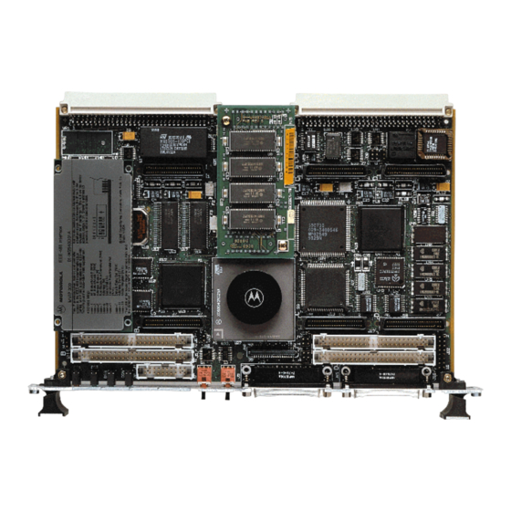
1559 9412 Figure 1-1. MVME162FX Block Diagram Functional Description This section covers only a few specific features of the MVME162FX. A complete functional description of the major blocks on the MVME162FX Embedded Controller is provided in the MVME162FX Embedded Controller Installation and Use manual. -
Page 28: No-Vmebus-Interface Option
Board Description and Memory Maps No-VMEbus-Interface Option The MVME162FX can be operated as an embedded controller without the VMEbus interface. For this option, the VMEchip2 and the VMEbus buffers are not populated. Also, the bus grant daisy chain and the interrupt acknowledge daisy chain have zero-ohm bypass resistors installed. -
Page 29: Vmebus Interface And Vmechip2
162Bug package, MVME162Bug, in such models, be sure that jumper header J22 is configured for the EPROM memory map. Refer to Chapters 3 and 4 of the MVME162FX Installation and Use documentation, V162FXA, for further details. VMEbus Interface and VMEchip2 The local-bus-to-VMEbus interface and the VMEbus-to-local-bus interface are provided by the optional VMEchip2. -
Page 30: Memory Maps
The normal address range is defined by the Transfer Type (TT) signals on the local bus. On the MVME162FX, Transfer Types 0, 1, and 2 define the normal address range. Table 1-2 is the entire map from $00000000 to $FFFFFFFF. -
Page 31: Table 1-2. Local Bus Memory Map
Memory Maps Table 1-2. Local Bus Memory Map Software Address Range Devices Accessed Port Width Size Cache Note(s) Inhibit Programmable DRAM on board 4MB-16MB Programmable SRAM 128KB-2MB Programmable VMEbus A32/A24 D32/D16 Programmable IP a Memory D32-D8 64KB-8MB 2, 4 Programmable IP b Memory D32-D8 64KB-8MB... - Page 32 Board Description and Memory Maps Notes 1. Reset enables the decoder for this space of the memory map so that it will decode address spaces $FF800000-$FF9FFFFF and $00000000-$003FFFFF. The decode at 0 must be disabled in the MC2 chip before DRAM is enabled. DRAM is enabled with the DRAM Control Register at address $FFF42048, bit 24.
-
Page 33: Table 1-3. Local Bus I/O Devices Memory Map
Memory Maps The following table focuses on the Local I/O Devices portion of the local bus Main Memory Map. Table 1-3. Local Bus I/O Devices Memory Map Port Address Range Device Size Note(s) Width $FFF00000 - $FFF3FFFF Reserved 256KB $FFF40000 - $FFF400FF VMEchip2 (LCSR) 256B 1, 3... - Page 34 Board Description and Memory Maps Table 1-3. Local Bus I/O Devices Memory Map (Continued) Port Address Range Device Size Note(s) Width $FFF58A00 - $FFF58A7F Reserved 128B $FFF58A80 - $FFF58AFF Reserved 128B $FFF58B00 - $FFF58B7F Reserved 128B $FFF58B80 - $FFF58BFF Reserved 128B $FFF58C00 - $FFF58CFF Reserved...
-
Page 35: Detailed I/O Memory Maps
Memory Maps Notes 1. For a complete description of the register bits, refer to the data sheet for the specific chip. For a more detailed memory map, refer to the following detailed peripheral device memory maps. 2. The SCC is an 8-bit device located on an MC2 chip private data bus. - Page 36 82596CA Ethernet LAN chip 1-10 53C710 SCSI chip 1-11 MK48T08 BBRAM/TOD clock 1-12 BBRAM conÞguration area 1-13 TOD clock ManufacturersÕ errata sheets for the various chips are Note available by contacting your local Motorola sales representative. A non-disclosure agreement may be required. 1-14...
-
Page 37: Table 1-4. Vmechip2 Memory Map (Sheet 1 Of 3)
Memory Maps Table 1-4. VMEchip2 Memory Map (Sheet 1 of 3) VMEchip2 LCSR Base Address = $FFF40000 OFFSET: SLAVE ENDING ADDRESS 1 SLAVE ENDING ADDRESS 2 SLAVE ADDRESS TRANSLATION ADDRESS 1 SLAVE ADDRESS TRANSLATION ADDRESS 2 ADDER PRGM DATA2 MASTER ENDING ADDRESS 1 MASTER ENDING ADDRESS 2 MASTER ENDING ADDRESS 3 MASTER ENDING ADDRESS 4... - Page 38 Board Description and Memory Maps SLAVE STARTING ADDRESS 1 SLAVE STARTING ADDRESS 2 SLAVE ADDRESS TRANSLATION SELECT 1 SLAVE ADDRESS TRANSLATION SELECT 2 ADDER PRGM DATA1 MASTER STARTING ADDRESS 1 MASTER STARTING ADDRESS 2 MASTER STARTING ADDRESS 3 MASTER STARTING ADDRESS 4 MASTER ADDRESS TRANSLATION SELECT 4 MAST MAST...
-
Page 39: Table 1-4. Vmechip2 Memory Map (Sheet 2 Of 3)
Memory Maps Table 1-4. VMEchip2 Memory Map (Sheet 2 of 3) VMEchip2 LCSR Base Address = $FFF40000 OFFSET: BGTO GLOBAL TIME OFF TIME ON TIMER TICK TIMER 1 TICK TIMER 1 TICK TIMER 2 TICK TIMER 2 SCON PURS FAIL FAIL STAT PURS... - Page 40 Board Description and Memory Maps 1-18...
- Page 41 Memory Maps LOCAL PRESCALER ACCESS TIME OUT CLOCK ADJUST TIMER TIMER SELECT COMPARE REGISTER COUNTER COMPARE REGISTER COUNTER OVERFLOW OVERFLOW COUNTER 2 COUNTER 1 SCALER SPARE IRQ7 IRQ6 IRQ5 IRQ4 IRQ3 IRQ2 IRQ1 P ERROR IRQ1E TIC TIMER 2 TIC TIMER 1 IRQ LEVEL IRQ LEVEL IRQ LEVEL...
-
Page 42: Table 1-4. Vmechip2 Memory Map (Sheet 3 Of 3)
Board Description and Memory Maps Table 1-4. VMEchip2 Memory Map (Sheet 3 of 3) VMEchip2 GCSR Base Address = $FFF40100 Offsets Bit Numbers Local -bus CHIP REVISION CHIP ID LM3 LM2 LM1 LM0 SIG3 SIG2 SIG1 SIG0 RST SCON SYSFL GENERAL PURPOSE CONTROL AND STATUS REGISTER 0 GENERAL PURPOSE CONTROL AND STATUS REGISTER 1 GENERAL PURPOSE CONTROL AND STATUS REGISTER 2... -
Page 43: Table 1-5. Mc2 Chip Register Map
(reserved) LANC Interrupt LANC Bus Error Status Control Interrupt Control SCSI Error Status General Purpose MVME162FX SCSI Interrupt Inputs Version Control Tick Timer 3 Compare Register Tick Timer 3 Counter Register Tick Timer 4 Compare Register Tick Timer 4 Counter Register... -
Page 44: Table 1-6. Ip2 Chip Overall Memory Map
Board Description and Memory Maps The following memory map table includes all devices selected by the IP2 chip map decoder. Table 1-6. IP2 chip Overall Memory Map Address Range Selected Device Port Width Size Programmable IP_a/IP_ab Memory Space D32-D8 64KB-16MB Programmable IP_b Memory Space D16-D8... -
Page 45: Table 1-7. Ip2 Chip Memory Map - Control And Status Registers
Memory Maps Table 1-7. IP2 chip Memory Map - Control and Status Registers IP2 chip Base Address = $FFFBC000 Register Bit Names Register Register Offset Name CHIP ID CHIP REVISION RESERVED VECTOR BASE IP_a MEM a_BASE31 a_BASE30 a_BASE29 a_BASE28 a_BASE27 a_BASE26 a_BASE25 a_BASE24... - Page 46 Board Description and Memory Maps Table 1-7. IP2 chip Memory Map - Control and Status Registers (Continued) IP2 chip Base Address = $FFFBC000 Register Bit Names Register Register Offset Name IP_a a_ERR a_RT1 a_RT0 a_WIDTH1 a_WIDTH0 a_BTD a_MEN GENERAL CONTROL IP_b b_ERR b_RT1...
- Page 47 Memory Maps Table 1-7. IP2 chip Memory Map - Control and Status Registers (Continued) IP2 chip Base Address = $FFFBC000 Register Bit Names Register Register Offset Name DMAC for IndustryPack a, request 0. This register set is referred to as DMACa in the text. DMA_a DLBE IPEND...
- Page 48 Board Description and Memory Maps Table 1-7. IP2 chip Memory Map - Control and Status Registers (Continued) IP2 chip Base Address = $FFFBC000 Register Bit Names Register Register Offset Name DMAC for IndustryPack b, request 0 or for IndustryPack a, request 1. This register set is referred to as DMACb in the text. DMA_b DLBE IPEND...
- Page 49 Memory Maps Table 1-7. IP2 chip Memory Map - Control and Status Registers (Continued) IP2 chip Base Address = $FFFBC000 Register Bit Names Register Register Offset Name DMAC for IndustryPack c, request 0. This register set is referred to as DMACc in the text. DMA_c DLBE IPEND...
- Page 50 Board Description and Memory Maps Table 1-7. IP2 chip Memory Map - Control and Status Registers (Continued) IP2 chip Base Address = $FFFBC000 Register Bit Names Register Register Offset Name DMAC for IndustryPack d, request 0 or for IndustryPack c, request 1, and for PACER CLOCK. This register set, not including the Pacer Clock, is referred to as DMACd in the text.
- Page 51 Memory Maps Table 1-7. IP2 chip Memory Map - Control and Status Registers (Continued) IP2 chip Base Address = $FFFBC000 Register Bit Names Register Register Offset Name PACER INT ICLR CONTROL PACER GEN PLTY CONTROL PACER TIMER PACER TIMER 1-29...
-
Page 52: Table 1-8. Z85230 Scc Register Addresses
Board Description and Memory Maps Table 1-8. Z85230 SCC Register Addresses Z85230 SCC Register Address Port B Control $FFF45001 Port B Data $FFF45003 Port A Control $FFF45005 Port A Data $FFF45007 Note A bug in MVME162FXs that have MC2 chip revision $01 does not allow the data registers to be accessed directly. -
Page 53: Bbram/Tod Clock Memory Map
(TOD) clock, is defined by the chip hardware. The first area is reserved for user data. The second area is used by Motorola networking software. The third area may be used by an operating system. The fourth area is used by the MVME162FX board debugger (MVME162Bug). -
Page 54: Table 1-11. Mk48T08 Bbram/Tod Clock Memory Map
Board Description and Memory Maps Table 1-11. MK48T08 BBRAM/TOD Clock Memory Map Address Range Description Size (Bytes) $FFFC0000 - $FFFC0FFF User Area 4096 $FFFC1000 - $FFFC10FF Networking Area $FFFC1100 - $FFFC16F7 Operating System Area 1528 $FFFC16F8 - $FFFC1EF7 Debugger Area 2048 $FFFC1EF8 - $FFFC1FF7 ConÞguration Area... -
Page 55: Table 1-13. Tod Clock Memory Map
Memory Maps Table 1-12. BBRAM Configuration Area Memory Map (Continued) Address Range Description Size (Bytes) $FFFC1F86 - $FFFC1F8D IP c Board ID $FFFC1F8E - $FFFC1F95 IP c Board Serial Number $FFFC1F96 - $FFFC1F9D IP c Board PWB $FFFC1F9E - $FFFC1FA5 IP d Board ID $FFFC1FA6 - $FFFC1FAD IP d Board Serial Number... - Page 56 Board Description and Memory Maps The data structure of the configuration bytes starts at $FFFC1EF8 and is as follows. struct brdi_cnfg { char version[4]; char serial[12]; char id[16]; char pwa[16]; char speed[4]; char ethernet[6]; char fill[2]; char lscsiid[2]; char mem_pwb[8]; char mem_serial[8];...
- Page 57 Memory Maps 000000470476 3. Sixteen bytes are reserved for the board ID in ASCII format. For example, for an MVME162FX board with MC68040, SCSI, Ethernet, 4MB DRAM, and 512KB SRAM, this field contains: MVME162-513A (The 12 characters are followed by four blanks.) 4.
- Page 58 Board Description and Memory Maps 10. Eight bytes are reserved for the serial number assigned to the memory mezzanine board in ASCII format. 11. Eight bytes are reserved for the printed wiring board (PWB) number assigned to the serial port 2 personality board in ASCII format.
-
Page 59: Interrupt Acknowledge Map
The VMEchip2 includes a user-programmable map decoder for the VMEbus to local bus interface. The map decoder allows you to program the starting and ending address and the modifiers the MVME162FX responds to. VMEbus Short I/O Memory Map The VMEchip2 includes a user-programmable map decoder for the GCSR. -
Page 60: Software Support Considerations
Board Description and Memory Maps Software Support Considerations The MVME162FX is a complex board that interfaces to the VMEbus and SCSI bus. These multiple bus interfaces raise the issue of cache coherency and support of indivisible cycles. There are also many sources of bus error. -
Page 61: Sources Of Local Berr
Note The present MVME162FX models do not contain parity DRAM. The devices on the MVME162FX that are able to assert a local bus error are described below. Local Bus Time-out A Local Bus Time-out occurs whenever a local bus cycle does not complete within the programmed time (VMEbus bound cycles are not timed by the local bus timer). -
Page 62: Local Dram Parity Error
LWORD* low to a 16-bit board), a hardware error occurs on the VMEbus, or a VMEbus slave reports an access error (such as parity error). Local DRAM Parity Error The present MVME162FX models do not contain parity Note DRAM. When parity checking is enabled, the current bus master receives a bus error if it is accessing the local DRAM and a parity error occurs. -
Page 63: Description Of Error Conditions On The Mvme162Fx
Description of Error Conditions on the MVME162FX This section list the various error conditions that are reported by the MVME162FX hardware. A subsection heading identifies each type of error condition. A standard format gives a description of the error, indicates how notification of the error condition is made,... -
Page 64: Mpu Tea - Cause Unidentified
Comments: This can be caused by a VMEbus time-out, a VMEbus BERR, or an MVME162FX VMEbus access time-out. The latter is the time from when the VMEbus has been requested to when it is granted. MPU TEA - Cause Unidentified Description: An error occurred while the MPU was attempting an access. -
Page 65: Dmac Vmebus Error
This indicates the DMAC attempted to access a VMEbus address at which there was no resource or the VMEbus slave returned a BERR signal. DMAC Parity Error Note The present MVME162FX models do not contain parity DRAM. Description: Parity error while the DMAC was reading DRAM. MPU Notification: DMAC interrupt (when enabled). -
Page 66: Dmac Off-Board Error
Board Description and Memory Maps DMAC Off-board Error Description: Error encountered while the local bus side of the DMAC was attempting to go to the VMEbus. MPU Notification: DMAC interrupt (when enabled). Status: The DLOB bit is set in the DMAC Status Register (address $FFF40048 bit 4). -
Page 67: Dmac Tea - Cause Unidentified
If the TBL bit is set (address $FFF40048 bit 2) the error occurred during a command table access, otherwise the error occurred during a data access. LAN Parity Error The present MVME162FX models do not contain parity Note DRAM. Description: Parity error while the LANCE was reading DRAM MPU. -
Page 68: Lan Off-Board Error
The LANCE has no ability to respond to TEA so the error interrupt and status are provided in the MC2 chip. Control for the interrupt is in the MC2 chip LAN Error Interrupt Control Register ($FFF4202B). SCSI Parity Error The present MVME162FX models do not contain parity Note DRAM. 1-46... -
Page 69: Scsi Off-Board Error
Software Support Considerations Description: Parity error detected while the 53C710 was reading DRAM. MPU Notification: 53C710 Interrupt. Status: 53C710 DMA Status Register 53C710 DMA Interrupt Status Register MC2 chip SCSI Error Status Register ($FFF4202C). Comments: 53C710 interrupt enables are controlled in the 53C710 and in the MC2 chip SCSI Interrupt Control Register ($FFF4202F). -
Page 70: Example Of The Proper Use Of Bus Timers
Example of the Proper Use of Bus Timers In this example, the use of the bus timers is illustrated by describing the sequence of events when the MPU on one MVME162FX accesses the local bus memory on another MVME162FX using the VMEbus. -
Page 71: Mvme162Fx Mc68040 Indivisible Cycles
Before an MVME162FX access to another MVME162FX can complete, however, the VMEchip2 on the accessed MVME162FX must decode a slave access and request the local bus of the second MVME162FX. When the local bus is granted (any in-process onboard transfers have completed) then the local bus timer of the accessed MVME162FX starts. -
Page 72: Illegal Access To Ip Modules From External Vmebus Masters
Illegal Access to IP Modules from External VMEbus Masters When a device other than the local MVME162FX is operating as VMEbus master, access by that device to the local IP modules is subject to restrictions. -
Page 73: Introduction
2VMEchip2 Introduction This chapter defines the VMEchip2 ASIC, local bus to VMEbus interface chip. The VMEchip2 interfaces the local bus to the VMEbus. In addition to the VMEbus defined functions, the VMEchip2 includes a local bus to VMEbus DMA controller, VME board support features, and Global Control and Status Registers (GCSR) for interprocessor communications. - Page 74 VMEchip2 VMEbus Bus to Local Bus Interface: Ð Programmable VMEbus map decoder. Ð Programmable AM decoder. Ð Programmable local bus snoop enable. Ð Simple VMEbus to local bus address translation. Ð 8-bit, 16-bit and 32-bit VMEbus data width. Ð 8-bit, 16-bit and 32-bit block transfer. Ð...
- Page 75 Introduction Release-On-End-Of-Data (ROEOD); Software-configured BR0-BR3 request levels; and Software enabled bus-tenure timer. VMEbus Interrupter: Ð Software-configured IRQ1-IRQ7 interrupt request level. Ð 8-bit software-programmed status/ID register. VMEbus System Controller: Ð Arbiter with software-configured arbitration modes: Priority (PRI), Round-Robin-Select (RRS), and Single-level (SGL). Ð...
-
Page 76: Functional Blocks
VMEchip2 Functional Blocks The following sections provide an overview of the functions provided by the VMEchip2. See Figure 2-1 for a block diagram of the VMEchip2. A detailed programming model for the local control and status registers (LCSR) is provided in the following section. A detailed programming model for the global control and status registers (GCSR) is provided in the next section. -
Page 77: Figure 2-1. Vmechip2 Block Diagram
Functional Blocks Figure 2-1. VMEchip2 Block Diagram... - Page 78 VMEchip2 Using programmable map decoders with programmable attribute bits, the local bus to VMEbus interface can be configured to provide the following VMEbus capabilities: Addressing capabilities: A16, A24, A32 Data transfer capabilities: D08, D16, D32 The local bus slave includes six local bus map decoders for accessing the VMEbus.
- Page 79 Functional Blocks When write posting is enabled, the VMEchip2 stores the local bus address and data and then acknowledges the local bus master. The local bus is then free to perform other operations while the VMEbus master requests the VMEbus and performs the requested operation. The write post buffer stores one byte, two-byte, four-byte, or one cache line (four four-bytes).
-
Page 80: Local Bus To Vmebus Requester
VMEchip2 VMEbus. If the data transfer does not begin before the timer times out, the timer drives the local bus error signal, and sets the appropriate status bit in the Local Control and Status Register (LCSR). Using control bits in the LCSR, the timer can be disabled, or it can be enabled to drive the local bus error signal after 64 µs, 1 ms, or 32 ms. -
Page 81: Vmebus To Local Bus Interface
Functional Blocks The local bus to VMEbus requester in the VMEchip2 implements a fair mode. By setting the LVFAIR bit, the requester refrains from requesting the VMEbus until it detects its assigned request line in its negated state. The local bus to VMEbus requester attempts to release the VMEbus when the requested data transfer operation is complete, the DWB pin is negated, the DWB bit in the LCSR is negated and the bus is not being held by a lock cycle. - Page 82 VMEchip2 Adhering to the IEEE 1014-87 VMEbus Standard, the slave can withstand address-only cycles, as well as address pipelining, and respond to unaligned transfers. Using programmable map decoders, it can be configured to provide the following VMEbus capabilities: Addressing capabilities: A24, A32 Data transfer capabilities: D08(EO), D16, D32, D8/BLT, D16/BLT, D32/BLT, D64/BLT (BLT = block transfer)
-
Page 83: Local Bus To Vmebus Dma Controller
Functional Blocks The alternate address register also provides the upper eight bits of the local address when the VMEbus slave cycle is A24. The local bus master requests the local bus and executes cycles as required. To reduce local bus loading and improve performance it always attempts to transfer data using a burst transfer as defined by the MC68040. - Page 84 VMEchip2 Data transfer capabilities: D16, D32, D16/BLT, D32/BLT, D64/BLT (BLT = block transfer) Using the DMA AM control register, the address modifier code that the VMEbus DMA controller places on the VMEbus can be programmed under software control. In addition, the DMAC can be programmed to execute block-transfer cycles over the VMEbus.
-
Page 85: No Address Increment Dma Transfers
VMEbus address. The DMA controller also allows DMA transfers without incrementing the local bus address, however the MVME162FX does not have any onboard devices that benefit from not incrementing the local bus address. The transfer mode on the VMEbus may be D16, D16/BLT, D32, D32/BLT or D64/BLT. -
Page 86: Dmac Vmebus Requester
VMEchip2 support the various port sizes and to allow transfers which are not an even byte count or start at an odd address, with respect to the port size. A 16-bit device should respond with VA<1> high or low. Devices on the local bus should respond to any combination of LA<3..2>. -
Page 87: Tick And Watchdog Timers
Functional Blocks Requiring no external jumpers, the chip provides the means for software to program the DMAC requester to request the bus on any one of the four bus request levels, automatically establishing the bus grant daisy-chains for the three inactive levels. The DMAC requester requests the bus as required to transfer data to or from the FIFO buffer. -
Page 88: Tick Timers
VMEchip2 Software is required to load the appropriate constant, depending upon the local bus clock, following reset to ensure proper operation of the prescaler. Tick Timers The VMEchip2 includes two general purpose tick timers. These timers can be used to generate interrupts at various rates or the counters can be read at various times for interval timing. -
Page 89: Watchdog Timer
Functional Blocks Watchdog Timer The watchdog timer has a 4-bit counter, four clock select bits, an enable bit, a local reset enable bit, a SYSRESET enable bit, a board fail enable bit, counter reset bit, WDTO status bit, and WDTO status reset bit. -
Page 90: Vmebus System Controller
VMEchip2 should be enabled. All boards in the system which are not participating in the broadcast interrupt function should not drive or respond to any signals on the IRQ1 signal line. There are two ways to broadcast an IRQ1 interrupt. The VMEbus interrupter in the VMEchip2 may be programmed to generate a level one interrupt. -
Page 91: Iack Daisy-Chain Driver
Functional Blocks IACK Daisy-Chain Driver Complying with the latest revision of the VMEbus specification, the System Controller includes an IACK Daisy-Chain Driver, ensuring that the timing requirements of the IACK daisy-chain are satisfied. Bus Timer The Bus Timer is enabled/disabled by software to terminate a VMEbus cycle by asserting BERR if any of the VMEbus data strobes is maintained in its asserted state for longer than the programmed time-out period. -
Page 92: Local Bus Interrupter And Interrupt Handler
VMEchip2 Local Bus Interrupter and Interrupt Handler There are 31 interrupt sources in the VMEchip2: VMEbus ACFAIL, switch, VMEbus SYSFAIL, write post bus error, external ABORT input, VMEbus IRQ1 edge-sensitive, VMEchip2 VMEbus interrupter acknowledge, tick timer 2-1, DMAC done, GCSR SIG3- 0, GCSR location monitor 1-0, software interrupts 7-0, and VMEbus IRQ7-1. - Page 93 Functional Blocks The DMAC interrupter is an edge-sensitive interrupter connected to the DMAC. The GCSR SIG3-0 interrupters are edge-sensitive interrupters connected to the output of the signal bits in the GCSR. The location monitor interrupters are edge-sensitive interrupters connected to the location monitor bits in the GCSR. The software 7-0 interrupters can be set by software to generate interrupts.
-
Page 94: Global Control And Status Registers
VMEchip2 Global Control and Status Registers The VMEchip2 includes a set of registers that are accessible from both the VMEbus and the local bus. These registers are provided to aid in interprocessor communications over the VMEbus. These registers are fully described in a later section. LCSR Programming Model This section defines the programming model for the Local Control and Status Registers (LCSR) in the VMEchip2. - Page 95 LCSR Programming Model Line 4 defines the operations possible on the register bits as follows: This bit is a read-only status bit. This bit is readable and writable. W/AC This bit can be set and it is automatically cleared. This bit can also be read.
-
Page 96: Table 2-1. Vmechip2 Memory Map - Lcsr Summary (Sheet 1 Of 2)
VMEchip2 Table 2-1. VMEchip2 Memory Map - LCSR Summary (Sheet 1 of 2) VMEchip2 LCSR Base Address = $FFF40000 OFFSET: SLAVE ENDING ADDRESS 1 SLAVE ENDING ADDRESS 2 SLAVE ADDRESS TRANSLATION ADDRESS 1 SLAVE ADDRESS TRANSLATION ADDRESS 2 ADDER PRGM DATA2 MASTER ENDING ADDRESS 1 MASTER ENDING ADDRESS 2... - Page 97 LCSR Programming Model SLAVE STARTING ADDRESS 1 SLAVE STARTING ADDRESS 2 SLAVE ADDRESS TRANSLATION SELECT 1 SLAVE ADDRESS TRANSLATION SELECT 2 ADDER PRGM DATA1 MASTER STARTING ADDRESS 1 MASTER STARTING ADDRESS 2 MASTER STARTING ADDRESS 3 MASTER STARTING ADDRESS 4 MASTER ADDRESS TRANSLATION SELECT 4 MAST MAST...
-
Page 98: Table 2-1. Vmechip2 Memory Map - Lcsr Summary (Sheet 2 Of 2)
VMEchip2 Table 2-1. VMEchip2 Memory Map - LCSR Summary (Sheet 2 of 2) VMEchip2 LCSR Base Address = $FFF40000 OFFSET: BGTO GLOBAL TIME OFF TIME ON TIMER TICK TIMER 1 TICK TIMER 1 TICK TIMER 2 TICK TIMER 2 SCON PURS FAIL FAIL... - Page 99 LCSR Programming Model LOCAL PRESCALER ACCESS TIME OUT CLOCK ADJUST TIMER TIMER SELECT COMPARE REGISTER COUNTER COMPARE REGISTER COUNTER OVERFLOW OVERFLOW COUNTER 2 COUNTER 1 SCALER SPARE IRQ7 IRQ6 IRQ5 IRQ4 IRQ3 IRQ2 IRQ1 P ERROR IRQ1E TIC TIMER 2 TIC TIMER 1 IRQ LEVEL IRQ LEVEL...
-
Page 100: Programming The Vmebus Slave Map Decoders
VMEchip2 Programming the VMEbus Slave Map Decoders This section includes programming information for the VMEbus to local bus map decoders. The VMEbus to local bus interface allows off-board VMEbus masters access to local onboard resources. The address of the local resources as viewed from the VMEbus is controlled by the VMEbus slave map decoders, which are part of the VMEbus to local bus interface. - Page 101 LCSR Programming Model and starting and ending address registers should be programmed first, and then the map decoders should be enabled by programming the address modifier select registers. A VMEbus slave map decoder is programmed by loading the starting address of the segment into the starting address register and the ending address of the segment into the ending address register.
- Page 102 VMEchip2 enabled, the local bus address is generated by adding the offset value to the VMEbus address lines VA<31..16>. The offset is the value in the address translation/offset register. If the VMEbus transfer is A24, then the VMEbus address lines VA<31..24> are forced to 0 before the add.
-
Page 103: Vmebus Slave Ending Address Register 1
LCSR Programming Model VMEbus Slave Ending Address Register 1 ADR/SIZ $FFF40000 (16 bits of 32) . . . Ending Address Register 1 NAME OPER RESET 0 PS This register is the ending address register for the first VMEbus to local bus map decoder. VMEbus Slave Starting Address Register 1 ADR/SIZ $FFF40000 (16 bits of 32) -
Page 104: Vmebus Slave Starting Address Register 2
VMEchip2 VMEbus Slave Starting Address Register 2 ADR/SIZ $FFF40004 (16 bits of 32) . . . NAME Starting Address Register 2 OPER RESET 0 PS This register is the starting address register for the second VMEbus to local bus map decoder. VMEbus Slave Address Translation Address Offset Register 1 ADR/SIZ $FFF40008 (16 bits of 32) -
Page 105: Vmebus Slave Address Translation Select Register 1
LCSR Programming Model VMEbus Slave Address Translation Select Register 1 ADR/SIZ $FFF40008 (16 bits of 32) . . . NAME Address Translation Select Register 1 OPER RESET 0 PS This register is the address translation select register for the first VMEbus to local bus map decoder. -
Page 106: Vmebus Slave Address Translation Address Offset Register 2
VMEchip2 VMEbus Slave Address Translation Address Offset Register 2 ADR/SIZ $FFF4000C (16 bits of 32) . . . NAME Address Translation Address Offset Register 2 OPER 0 PS RESET This register is the address translation address register for the second VMEbus to local bus map decoder. It should be programmed to the local bus starting address. -
Page 107: Vmebus Slave Write Post And Snoop Control Register 2
LCSR Programming Model VMEbus Slave Write Post and Snoop Control Register 2 ADR/SIZ $FFF40010 (8 bits [4 used] of 32) NAME ADDER2 SNP2 OPER RESET 0 PS 0 PS 0 PS This register is the slave write post and snoop control register for the second VMEbus to local bus map decoder. -
Page 108: Vmebus Slave Address Modifier Select Register 2
VMEchip2 VMEbus Slave Address Modifier Select Register 2 ADR/SIZ $FFF40010 (8 bits of 32) NAME OPER RESET 0 PSL 0 PSL 0 PSL 0 PSL 0 PSL 0 PSL 0 PSL 0 PSL This register is the address modifier select register for the second VMEbus to local bus map decoder. -
Page 109: Vmebus Slave Write Post And Snoop Control Register 1
LCSR Programming Model When this bit is high, the second map decoder responds to VMEbus A32 (extended) access cycles. When this bit is low, the second map decoder does not respond to VMEbus A32 access cycles. When this bit is high, the second map decoder responds to VMEbus user (non-privileged) access cycles. - Page 110 VMEchip2 Write - Sink data Read - Supply dirty data and leave dirty Write - Invalidate Read - Supply dirty data and mark invalid Snoop inhibited ADDER1 When this bit is high, the adder is used for address translation. When this bit is low, the adder is not used for address translation.
-
Page 111: Programming The Local Bus To Vmebus Map Decoders
LCSR Programming Model When this bit is high, the first map decoder responds to VMEbus D64 block access cycles. When this bit is low, the first map decoder does not respond to VMEbus D64 block access cycles. When this bit is high, the first map decoder responds to VMEbus A24 (standard) access cycles. - Page 112 VMEchip2 space. The second I/O map decoder provides an A24/D16 space at $F000000 to $F0FFFFFF and an A32/D16 space at $F1000000 to $FF7FFFFF. A programmable segment may vary in size from 64KB to 4GB in increments of 64KB. Address translation for the fourth segment is provided by the address translation registers which allow the upper 16 bits of the VMEbus address to be provided by the address translation address register rather than the upper 16 bits of the local...
- Page 113 LCSR Programming Model The address translation address register and the address translation select register operate in the following way. If a bit in the address translation select register is set, then the corresponding VMEbus address line is driven from the corresponding bit in the address translation address register.
-
Page 114: Local Bus Slave (Vmebus Master) Ending Address Register 1
VMEchip2 Local Bus Slave (VMEbus Master) Ending Address Register 1 ADR/SIZ $FFF40014 (16 bits of 32) . . . NAME Ending Address Register 1 OPER RESET 0 PS This register is the ending address register for the first local bus to VMEbus map decoder. -
Page 115: Local Bus Slave (Vmebus Master) Starting Address Register 3
LCSR Programming Model Local Bus Slave (VMEbus Master) Starting Address Register 2 ADR/SIZ $FFF40018 (16 bits of 32) . . . NAME Starting Address Register 2 OPER RESET 0 PS This register is the starting address register for the second local bus to VMEbus map decoder. - Page 116 VMEchip2 Local Bus Slave (VMEbus Master) Ending Address Register 4 ADR/SIZ $FFF40020 (16 bits of 32) . . . NAME Ending Address Register 4 OPER RESET 0 PS This register is the ending address register for the fourth local bus to VMEbus map decoder.
-
Page 117: Local Bus Slave (Vmebus Master) Address Translation Select Register 4
LCSR Programming Model Local Bus Slave (VMEbus Master) Address Translation Select Register 4 ADR/SIZ $FFF40024 (16 bits of 32) . . . NAME Address Translation Select Register 4 OPER RESET 0 PS This register is the address translation select register for the fourth local bus to VMEbus bus map decoder. -
Page 118: Local Bus Slave (Vmebus Master) Attribute Register 3
VMEchip2 Local Bus Slave (VMEbus Master) Attribute Register 3 ADR/SIZ $FFF40028 (8 bits of 32) NAME OPER RESET 0 PS 0 PS O PS This register is the attribute register for the third local bus to VMEbus bus map decoder. These bits define the VMEbus address modifier codes the VMEbus master uses for the segment defined by map decoder 3. - Page 119 LCSR Programming Model These bits define the VMEbus address modifier codes the VMEbus master uses for the segment defined by map decoder 2. Since the local bus to VMEbus interface does not support block transfers, the block transfer address modifier codes should not be used.
-
Page 120: Vmebus Slave Gcsr Group Address Register
GCSR Group These bits define the group portion of the GCSR address. These bits are compared with VMEbus address lines A8 through A15. The recommended group address for the MVME162FX is $D2. VMEbus Slave GCSR Board Address Register ADR/SIZ $FFF4002C (4 bits of 32) . -
Page 121: Local Bus To Vmebus Enable Control Register
LCSR Programming Model GCSR Board These bits define the board number portion of the GCSR address. These bits are compared with VMEbus address lines A4 through A7. The GCSR is enabled by values $0 through $E. The address $XXFY in the VMEbus A16 space is reserved for the location monitors LM0 through LM3. -
Page 122: Local Bus To Vmebus I/O Control Register
VMEchip2 Local Bus to VMEbus I/O Control Register ADR/SIZ $FFF4002C (8 bits of 32) NAME I2EN I2WP I2SU I2PD I1EN I1D16 I1WP I1SU OPER RESET 0 PSL 0 PS O PS 0 PS 0 PS O PS 0 PS O PS This register controls the VMEbus short I/O map and the F page ($F0000000 through $FF7FFFFF) I/O map. -
Page 123: Rom Control Register
A32/D16. When this bit is low, the F page is disabled. ROM Control Register ADR/SIZ $FFF4002C NAME SIZE BSSPD ASPD OPER 0 PS 0 PS 0 PS RESET This function is not used on the MVME162FX. 2-51... -
Page 124: Programming The Vmechip2 Dma Controller
2VMEchip2 2LCSR Programming Model VMEchip2 Programming the VMEchip2 DMA Controller This section includes programming information on the DMA controller, VMEbus interrupter, MPU status register, and local bus to VMEbus requester register. The VMEchip2 features a local bus -VMEbus DMA controller (DMAC). -
Page 125: Dmac Registers
LCSR Programming Model Once the DMAC is enabled, the counter and control registers should not be modified by software. When the command chaining mode is used, the list of commands must be in local 32-bit memory and the entries must be four-byte aligned. A DMAC command list includes one or more DMAC command packets. -
Page 126: Prom Decoder, Sram And Dma Control Register
This VMEchip2 bit is not used on the MVME162FX. Its function is performed by the ROM0 bit in the PROM Access Time Control Register in the MC2 chip. Refer to Chapter 3. WAIT RMW This function is not used on the MVME162FX. 2-54... -
Page 127: Local Bus To Vmebus Requester Control Register
LCSR Programming Model Local Bus to VMEbus Requester Control Register ADR/SIZ $FFF40030 (8 bits [7 used] OF 32) ROBN LVFAIR LVRWD LVREQL NAME OPER RESET 0 PS 0 PS 0 PSL 0 PS 0 PS 0 PS This register controls the VMEbus request level, the request mode, and release mode for the local bus to VMEbus interface. -
Page 128: Dmac Control Register 1 (Bits 0-7)
VMEchip2 to the release mode programmed in the LVRWD bit. When the VMEbus has been acquired, the DHB bit is set. When this bit is high, the VMEbus has been acquired in response to the DWB bit being set. When the DWB bit is cleared, this bit is cleared. -
Page 129: Dmac Control Register 2 (Bits 8-15)
LCSR Programming Model Release when the time on timer has expired and a BRx* signal is active on the VMEbus. Release when the time on timer has expired. Release when a BRx* signal is active on the VMEbus. Release when a BRx* signal is active on the VMEbus or the time on timer has expired. - Page 130 VMEchip2 When this bit is high, the DMAC executes D16 cycles on the VMEbus. When this bit is low, the DMAC executes D32/D64 cycles on the VMEbus. TVME This bit defines the direction in which the DMAC transfers data. When this bit is high, data is transferred to the VMEbus.
-
Page 131: Dmac Control Register 2 (Bits 0-7)
LCSR Programming Model DMAC Control Register 2 (bits 0-7) ADR/SIZ $FFF40034 (8 bits of 32) VME AM NAME OPER RESET 0 PS 0 PS This portion of the control register is loaded by the processor or the DMAC when it loads the command word from the command packet. -
Page 132: Dmac Local Bus Address Counter
VMEchip2 The DMAC executes D64 block transfer cycles on the VMEbus. In the block transfer mode, the DMAC may execute byte, two- byte and four-byte cycles at the beginning and ending of a transfer in non-block transfer mode. If the D16 bit is set, the DMAC executes D16 block transfers. -
Page 133: Dmac Vmebus Address Counter
LCSR Programming Model DMAC VMEbus Address Counter ADR/SIZ $FFF4003C (32 bits) . . . DMAC VMEbus Address Counter NAME OPER RESET 0 PS In the direct mode, this counter is programmed with the starting address of the data in VMEbus memory. DMAC Byte Counter ADR/SIZ $FFF40040 (32 bits) -
Page 134: Vmebus Interrupter Control Register
VMEchip2 Table Address Counter ADR/SIZ $FFF40044 (32 bits) . . . NAME Table Address Counter OPER RESET 0 PS In the command chaining mode, this counter should be loaded by the processor with the starting address of the list of commands. This register gets reloaded by the DMAC with the starting address of the current command. -
Page 135: Vmebus Interrupter Vector Register
LCSR Programming Model is used. Normal VMEbus interrupts should never be cleared. This bit always reads 0 and writing a 0 to this bit has no effect. IRQ1S These bits control the function of the IRQ1 signal line on the VMEbus: The IRQ1 signal from the interrupter is connected to the IRQ1 signal line on the VMEbus. -
Page 136: Mpu Status And Dma Interrupt Count Register
DRAM data transfer. This bit is cleared by writing a one to the MCLR bit in this register. This bit is not defined for MVME162FX implementation. When this bit is set, the MPU received a TEA and MLBE additional status was not provided. -
Page 137: Dmac Status Register
When this bit is set, the DMAC received a TEA and the status indicated a parity error during a DRAM data transfer. This bit is cleared when the DMAC is enabled. This bit is not defined for MVME162FX implementation. 2-65... -
Page 138: Programming The Tick And Watchdog Timers
VMEchip2 When this bit is set, the DMAC received a TEA and DLBE additional status was not provided. This bit is cleared when the DMAC is enabled. MLTO When this bit is set, the MPU received a TEA and the status indicated a local bus time-out. -
Page 139: Dmac Ton/Toff Timers And Vmebus Global Time-Out Control Register
LCSR Programming Model DMAC Ton/Toff Timers and VMEbus Global Time-out Control Register ADR/SIZ $FFF4004C (8 bits of 32) TIME OFF TIME ON VGTO NAME OPER RESET 0 PS 0 PS 0 PS This register controls the DMAC time off timer, the DMAC time on timer, and the VMEbus global time-out timer. -
Page 140: Vme Access, Local Bus, And Watchdog Time-Out Control Register
VMEchip2 VME Access, Local Bus, and Watchdog Time-out Control Register ADR/SIZ $FFF4004C (8 bits of 32) NAME VATO LBTO WDTO OPER 0 PS 0 PS 0 PS RESET WDTO These bits define the watchdog time-out period: Bit Encoding Time-out Bit Encoding Time-out 512 µs 128 ms... -
Page 141: Prescaler Control Register
LCSR Programming Model Prescaler Control Register ADR/SIZ $FFF4004C (8 bits of 32) . . . Prescaler Adjust NAME OPER RESET $DF P The prescaler provides the various clocks required by the counters and timers in the VMEchip2. In order to specify absolute times from these counters and timers, the prescaler must be adjusted for different local bus clocks. -
Page 142: Tick Timer 1 Compare Register
VMEchip2 Tick Timer 1 Compare Register ADR/SIZ $FFF40050 (32 bits) . . . Tick timer 1 Compare Register NAME OPER RESET The tick timer 1 counter is compared to this register. When they are equal, an interrupt is sent to the local bus interrupter and the overflow counter is incremented. -
Page 143: Tick Timer 2 Compare Register
LCSR Programming Model Tick Timer 2 Compare Register ADR/SIZ $FFF40058 (32 bits) . . . Tick timer 2 Compare Register NAME OPER RESET The tick timer 2 counter is compared to this register. When they are equal, an interrupt is sent to the local bus interrupter and the overflow counter is incremented. -
Page 144: Tick Timer 2 Compare Register
VMEchip2 0LCSR Programming Model Tick Timer 2 Compare Register ADR/SIZ $FFF40058 (32 bits) . . . NAME Tick timer 2 Compare Register OPER RESET The tick timer 2 counter is compared to this register. When they are equal, an interrupt is sent to the local bus interrupter and the overflow counter is incremented. -
Page 145: Board Control Register
LCSR Programming Model Board Control Register ADR/SIZ $FFF40060 (8 bits [7 used] of 32) SCON SFFL BRFLI PURS CPURS BDFLO RSWE NAME OPER RESET 1 PSL 0 PS 1 PSL RSWE switch enable bit is used with the ÔÔno RESET VMEbus interfaceÕÕ... -
Page 146: Watchdog Timer Control Register
VMEchip2 Watchdog Timer Control Register ADR/SIZ $FFF40060 (8 bits of 32) SRST WDCS WDCC WDTO WDBFE WDS/L WDRSE WDEN NAME OPER RESET 0 PS 0 PSL 0 PSL 1 PSL 0 PSL WDEN When this bit is high, the watchdog timer is enabled. When this bit is low, the watchdog timer is not enabled. -
Page 147: Tick Timer 2 Control Register
LCSR Programming Model When this bit is set high, the watchdog time-out WDCS status bit (WDTO bit in this register) is cleared. SRST When this bit is set high, a SYSRESET signal is generated on the VMEbus. SYSRESET resets the VMEchip2 and clears this bit. -
Page 148: Tick Timer 1 Control Register
VMEchip2 Tick Timer 1 Control Register ADR/SIZ $FFF40060 (8 bits of 32) COVF NAME OPER RESET 0 PS 0 PS 0 PS 0 PS When this bit is high, the counter increments. When this bit is low, the counter does not increment. When this bit is high, the counter is reset to zero when it compares with the compare register. -
Page 149: Programming The Local Bus Interrupter
2VMEchip2 LCSR Programming Model VMEchip2 Programming the Local Bus Interrupter The local bus interrupter is used by devices that wish to interrupt the local bus. There are 31 devices that can interrupt the local bus through the VMEchip2. In the general case, each interrupter has a level select register, an enable bit, a status bit, a clear bit, and for the software interrupts, a set bit. -
Page 150: Table 2-3. Local Bus Interrupter Summary
VMEchip2 Table 2-3. Local Bus Interrupter Summary Priority for Interrupt Vector Simultaneous Interrupts VMEbus IRQ1 External Lowest VMEbus IRQ2 External VMEbus IRQ3 External VMEbus IRQ4 External VMEbus IRQ5 External VMEbus IRQ6 External VMEbus IRQ7 External Spare Software 0 Software 1 Software 2 Software 3 Software 4... - Page 151 DMAC VMEbus Interrupter Acknowledge Tick Timer 1 Tick Timer 2 VMEbus IRQ1 Edge- Sensitive (Not used on MVME162FX) VMEbus Master Write Post Error VMEbus SYSFAIL (Not used on MVME162FX) VMEbus ACFAIL Highest Notes 1. X = The contents of vector base register 0.
-
Page 152: Local Bus Interrupter Status Register (Bits 24-31)
The interrupt status bits are: Tick timer 1 interrupt TIC1 TIC2 Tick timer 2 interrupt VI1E VMEbus IRQ1 edge-sensitive interrupt Not used on MVME162FX VMEbus master write post error interrupt SYSF VMEbus SYSFAIL interrupt Not used on MVME162FX VMEbus ACFAIL interrupt 2-80... -
Page 153: Local Bus Interrupter Status Register (Bits 16-23)
LCSR Programming Model Local Bus Interrupter Status Register (bits 16-23) ADR/SIZ $FFF40068 (8 bits of 32) SIG3 SIG2 SIG1 SIG0 NAME OPER RESET 0 PSL 0 PSL 0 PSL 0 PSL 0 PSL 0 PSL 0 PSL 0 PSL This register is the local bus interrupter status register. When an interrupt status bit is high, a local bus interrupt is being generated. -
Page 154: Local Bus Interrupter Status Register (Bits 8-15)
VMEchip2 Local Bus Interrupter Status Register (bits 8-15) ADR/SIZ $FFF40068 (8 bits of 32) NAME OPER RESET 0 PSL 0 PSL 0 PSL 0 PSL 0 PSL 0 PSL 0 PSL 0 PSL This register is the local bus interrupter status register. When an interrupt status bit is high, a local bus interrupt is being generated. -
Page 155: Local Bus Interrupter Status Register (Bits 0-7)
LCSR Programming Model Local Bus Interrupter Status Register (bits 0-7) ADR/SIZ $FFF40068 (8 bits of 32) SPARE VME7 VME6 VME5 VME4 VME3 VME2 VME1 NAME OPER RESET 0 PSL 0 PSL 0 PSL 0 PSL 0 PSL 0 PSL 0 PSL 0 PSL This register is the local bus interrupter status register. -
Page 156: Local Bus Interrupter Enable Register (Bits 24-31)
ETIC1 Enable tick timer 1 interrupt Enable tick timer 2 interrupt ETIC2 Enable VMEbus IRQ1 edge-sensitive interrupt EVI1E Not used on MVME162FX EMWP Enable VMEbus master write post error interrupt ESYSF Enable VMEbus SYSFAIL interrupt Not used on MVME162FX EACF... -
Page 157: Local Bus Interrupter Enable Register (Bits 16-23)
LCSR Programming Model Local Bus Interrupter Enable Register (bits 16-23) ADR/SIZ $FFF4006C (8 bits of 32) EVIA EDMA ESIG3 ESIG2 ESIG1 ESIG0 ELM1 ELM0 NAME OPER RESET 0 PSL 0 PSL 0 PSL 0 PSL 0 PSL 0 PSL 0 PSL 0 PSL This register is the local bus interrupter enable register. -
Page 158: Local Bus Interrupter Enable Register (Bits 8-15)
VMEchip2 Local Bus Interrupter Enable Register (bits 8-15) ADR/SIZ $FFF4006C (8 bits of 32) ESW7 ESW6 ESW5 ESW4 ESW3 ESW2 ESW1 ESW0 NAME OPER RESET 0 PSL 0 PSL 0 PSL 0 PSL 0 PSL 0 PSL 0 PSL 0 PSL This is the local bus interrupter enable register. -
Page 159: Local Bus Interrupter Enable Register (Bits 0-7)
LCSR Programming Model Local Bus Interrupter Enable Register (bits 0-7) ADR/SIZ $FFF4006C (8 bits of 32) SPARE EIRQ7 EIRQ6 EIRQ5 EIRIQ4 EIRQ3 EIRQ2 EIRQ1 NAME OPER RESET 0 PSL 0 PSL 0 PSL 0 PSL 0 PSL 0 PSL 0 PSL 0 PSL This is the local bus interrupter enable register. -
Page 160: Software Interrupt Set Register (Bits 8-15)
VMEchip2 Software Interrupt Set Register (bits 8-15) ADR/SIZ $FFF40070 (8 bits of 32) SSW7 SSW6 SSW5 SSW4 SSW3 SSW2 SSW1 SSW0 NAME OPER RESET 0 PSL 0 PSL 0 PSL 0 PSL 0 PSL 0 PSL 0 PSL 0 PSL This register is used to set the software interrupts. -
Page 161: Interrupt Clear Register (Bits 16-23)
LCSR Programming Model Clear tick timer 2 interrupt CTIC2 Clear VMEbus IRQ1 edge-sensitive interrupt CVI1E Not used on MVME162FX CMWP Clear VMEbus master write post error interrupt CSYSF Clear VMEbus SYSFAIL interrupt Not used on MVME162FX CACF Clear VMEbus ACFAIL interrupt... -
Page 162: Interrupt Clear Register (Bits 8-15)
OPER RESET 0 PSL 0 PSL This register is used to define the level of the abort interrupt and the ACFAIL interrupt. AB LEVEL Not used on MVME162FX ACF LEVEL These bits define the level of the ACFAIL interrupt. 2-90... -
Page 163: Interrupt Level Register 1 (Bits 16-23)
This register is used to define the level of the VMEbus IRQ1 edge-sensitive interrupt and the level of the external (parity error) interrupt. IRQ1E LEVEL These bits define the level of the VMEbus IRQ1 edge-sensitive interrupt. PE LEVEL Not used on MVME162FX 2-91... -
Page 164: Interrupt Level Register 1 (Bits 0-7)
VMEchip2 Interrupt Level Register 1 (bits 0-7) ADR/SIZ $FFF40078 (8 bits [6 used] of 32) TICK2 LEVEL TICK1 LEVEL NAME OPER RESET 0 PSL 0 PSL This register is used to define the level of the tick timer 1 interrupt and the tick timer 2 interrupt. -
Page 165: Interrupt Level Register 2 (Bits 16-23)
LCSR Programming Model Interrupt Level Register 2 (bits 16-23) ADR/SIZ $FFF4007C (8 bits [6 used] of 32) SIG3 LEVEL SIG2 LEVEL NAME OPER RESET 0 PSL 0 PSL This register is used to define the level of the GCSR SIG2 interrupt and the GCSR SIG3 interrupt. -
Page 166: Interrupt Level Register 2 (Bits 0-7)
VMEchip2 Interrupt Level Register 2 (bits 0-7) ADR/SIZ $FFF4007C (8 bits [6 used] of 32) LM1 LEVEL LM0 LEVEL NAME OPER RESET 0 PSL 0 PSL This register is used to define the level of the GCSR LM0 interrupt and the GCSR LM1 interrupt. LM0 LEVEL These bits define the level of the GCSR LM0 interrupt. -
Page 167: Interrupt Level Register 3 (Bits 16-23)
LCSR Programming Model Interrupt Level Register 3 (bits 16-23) ADR/SIZ $FFF40080 (8 bits [6 used] of 32) SW5 LEVEL SW4 LEVEL NAME OPER RESET 0 PSL 0 PSL This register is used to define the level of the software 4 interrupt and the software 5 interrupt. -
Page 168: Interrupt Level Register 3 (Bits 0-7)
The VMEbus level 7 (IRQ7) interrupt may be mapped to any local bus interrupt level. VIRQ7 LEVEL These bits define the level of the VMEbus IRQ7 interrupt. SPARE LEVEL Not used on the MVME162FX 2-96... -
Page 169: Interrupt Level Register 4 (Bits 16-23)
LCSR Programming Model Interrupt Level Register 4 (bits 16-23) ADR/SIZ $FFF40084 (8 bits [6 used] of 32) VIRQ6 VIRQ5 LEVEL NAME OPER RESET 0 PSL 0 PSL This register is used to define the level of the VMEbus IRQ5 interrupt and the VMEbus IRQ6 interrupt. The VMEbus level 5 (IRQ5) interrupt and the VMEbus level 6 (IRQ6) interrupt may be mapped to any local bus interrupt level. -
Page 170: Interrupt Level Register 4 (Bits 0-7)
VMEchip2 Interrupt Level Register 4 (bits 0-7) ADR/SIZ $FFF40084 (8 bits [6 used] of 32) VIRQ2 VIRQ1 LEVEL NAME OPER RESET 0 PSL 0 PSL This register is used to define the level of the VMEbus IRQ1 interrupt and the VMEbus IRQ2 interrupt. The VMEbus level 1 (IRQ1) interrupt and the VMEbus level 2 (IRQ2) interrupt may be mapped to any local bus interrupt level. -
Page 171: I/O Control Register 1
Bits 16-19 control the direction of the four General Purpose I/O pins (GPIO0-3). Note The General Purpose I/O pins are not used on the MVME162FX. GPOEN0 Not used on MVME162FX GPOEN1 Not used on MVME162FX Not used on MVME162FX GPOEN2 GPOEN3... -
Page 172: I/O Control Register 2
GPIOO3 GPIOO2 GPIOO1 GPIOO0 GPIOI3 GPIOI2 GPIOI1 GPIOI0 OPER 0 PSL 0 PS 0 PS 0 PS RESET This function is not used on the MVME162FX. I/O Control Register 3 ADR/SIZ $FFF40088 (8 bits of 32) NAME GPI7 GPI6 GPI5... - Page 173 DISMST When this bit is high, the LED on the MVME162FX is lit when local bus reset is asserted or the VMEchip2 is driving local bus busy. When this bit is low, the LED on the MVME162FX is lit...
- Page 174 SRAM decoder in the VMEchip2 is enabled. Because the SRAM decoder in the VMEchip2 is not used on the MVME162FX, this bit must be set. This function is not used on the MVME162FX. This REVEROM bit must not be set.
-
Page 175: Gcsr Programming Model
GCSR Programming Model GCSR Programming Model This section describes the programming model for the Global Control and Status Registers (GCSR) in the VMEchip2. The local bus map decoder for the GCSR registers is included in the VMEchip2. The local bus base address for the GCSR is $FFF40100. The registers in the GCSR are 16 bits wide and they are byte accessible from both the VMEbus and the local bus. - Page 176 VMEchip2 The chip ID and revision registers are provided to allow software to determine the ID of the chip and its revision level. The VMEchip2 has a chip ID of ten. ID codes zero and one are used by the old VMEchip.
-
Page 177: Programming The Gcsr
GCSR Programming Model asserted, a local bus cycle may be aborted. The VMEchip2 is connected to both the local bus and the VMEbus and if the aborted cycle is bound for the VMEbus, erratic operation may result. Communications between the local processor and a VMEbus master should use interrupts or mailbox locations;... -
Page 178: Table 2-4. Vmechip2 Memory Map (Gcsr Summary)
VMEchip2 A summary of the GCSR is shown in Table 2-4. Table 2-4. VMEchip2 Memory Map (GCSR Summary) VMEchip2 GCSR Base Address = $FFF40100 Offsets Bit Numbers Local -bus CHIP REVISION CHIP ID LM3 LM2 LM1 LM0 SIG3 SIG2 SIG1 SIG0 RST SCON SYSFL GENERAL PURPOSE CONTROL AND STATUS REGISTER 0 GENERAL PURPOSE CONTROL AND STATUS REGISTER 1... -
Page 179: Vmechip2 Revision Register
01 PS This register is the VMEchip2 revision register. The revision level for the VMEchip2 starts at zero and is incremented if mask changes are required. The VMEchip2 used on the MVME162FX is revision $01 or greater. VMEchip2 ID Register... - Page 180 VMEchip2 The SIG0 bit is set when a VMEbus master writes a SIG0 one to it. When the SIG0 bit is set, an interrupt is sent to the local bus interrupter. The SIG0 bit is cleared when the local processor writes a one to the SIG0 bit in this register or the CSIG0 bit in the local interrupt clear register.
-
Page 181: Vmechip2 Board Status/Control Register
GCSR Programming Model This bit is cleared by an LM2 cycle on the VMEbus. This bit is set when the local processor or a VMEbus master writes a one to the LM0 bit in this register. This bit is cleared by an LM3 cycle on the VMEbus. This bit is set when the local processor or a VMEbus master writes a one to the LM3 bit in this register. - Page 182 VMEchip2 General Purpose Register 0 ADR/SIZ Local Bus: $FFF40108/VMEbus: $XXY4 (16 bits) . . . General Purpose Register 0 NAME OPER RESET 0 PS This register is a general purpose register that allows a local bus master to communicate with a VMEbus master. The function of this register is not defined by the hardware specification.
- Page 183 GCSR Programming Model General Purpose Register 2 ADR/SIZ Local Bus: $FFF40110/VMEbus: $XXY8 (16 bits) . . . General Purpose Register 2 NAME OPER RESET 0 PS This register is a general purpose register that allows a local bus master to communicate with a VMEbus master. The function of this register is not defined by the hardware specification.
- Page 184 VMEchip2 General Purpose Register 4 ADR/SIZ Local Bus: $FFF40118/VMEbus: $XXYC (16 bits) . . . General Purpose Register 4 NAME OPER RESET 0 PS This register is a general purpose register that allows a local bus master to communicate with a VMEbus master. The function of this register is not defined by the hardware specification.
-
Page 185: Introduction
3MC2 Chip Introduction The Memory Controller ASIC (MC2 chip) is one of three ASICs that are part of the MVME162FX hardware set. The MC2 chip is designed to operate synchronously with the MC68040 local bus clock at 25MHz or 32MHz. -
Page 186: Functional Description
162Bug package, MVME162Bug, in such models, be sure that jumper header J22 is configured for the EPROM memory map. Refer to Chapters 3 and 4 of the MVME162FX Installation and Use documentation, V162FXA, for further details. The MC2 chip executes multiple cycles to the eight-bit Flash/EPROM devices so that byte, word, or longword accesses are allowed. -
Page 187: Bbram Interface
Functional Description The 28F008SA has a ready/busy pin to interrupt the processor when certain commands have completed. The MC2 chip does not utilize this feature. Software has to poll the status register to determine device availability. The MC2 chip ASIC supports write cycles to EPROM memory space with a normal cycle termination by asserting transfer acknowledge. -
Page 188: Mc68040-Bus Master Support For 82596Ca
MC2 Chip MPU Port access enables the MPU to write to an internal, 32-bit 82596CA command register. This allows the MPU to do four things: 1. Write an alternate System Configuration Pointer address. 2. Write an alternative dump area pointer and perform a dump. 3. -
Page 189: Lanc Bus Error
Functional Description Read Size Transfer in progress LANC Bus Error The 82596CA does not provide a way to terminate a bus cycle with an error indication. Bus error are processed in the following way. The 82596CA interface logic monitors all bus cycles initiated by the 82596CA, and if a bus error is indicated (TAE* = 0 and TA* =1), the Back Off signal (BOFF*) to the 82596CA is asserted to keep the 82596CA off the local bus and prevent it from transmitting bad data... -
Page 190: Sram Memory Controller
100 ns devices. The size of the SRAM is initialized in the DRAM/SRAM Options Register when the MVME162FX is reset. SRAM performance at 25MHz is 5,3,3,3 for read and write cycle. SRAM performance at 32MHz is 6,4,4,4 for read cycles and 6,3,3,3 for write cycles. -
Page 191: Z85230 Scc Interface
The MC2 chip supports as many as four Z85230 devices. (There is only one Z85230 on the MVME162FX. Refer to the Board Level Hardware Description in the MVME162FX Embedded Controller Installation and Use manual.) The addresses for the devices are defined as follows. -
Page 192: Tick Timers
MC2 Chip Tick Timers The MC2 chip implements four 32-bit tick timers. These timers are identical to the timers in the VMEchip2. The timers run on a 1MHz clock which is derived from the processor clock by a prescaler. Each timer has a 32-bit counter, a 32-bit compare register, and a clear-on-compare enable bit. -
Page 193: Local Bus Timer
Memory Map of the MC2 chip Registers Local Bus Timer The MVME162FX provides a time-out function for the local bus. When the timer is enabled and a local bus access times out, a Transfer Error Acknowledge (TEA) signal is sent to the local bus master. -
Page 194: Table 3-2. Mc2 Chip Register Map
(reserved) LANC LANC Bus Error Status Interrupt Control Interrupt Control SCSI Error Status General Purpose MVME162FX SCSI Interrupt Inputs Version Control Tick Timer 3 Compare Register Tick Timer 3 Counter Register Tick Timer 4 Compare Register Tick Timer 4 Counter Register... -
Page 195: Programming Model
Programming Model Programming Model This section defines the programming model for the control and status registers (CSR) in the MC2 chip. The base address of the CSR is $FFF42000. The possible operations for each bit in the CSR are as follows: This bit is a read-only status bit. -
Page 196: Mc2 Chip Revision Register
MC2 Chip MC2 chip Revision Register ADR/SIZ $FFF42000 (8 bits) NAME OPER RESET 0 PL 0 PL 0 PL 0 PL 0 PL 0 PL 0 PL 1 PL RV7-RV0 The current value of the chip revision is $01. This register is read only. - Page 197 PowerPC. When this bit is low, the IPL signal outputs are compatible with the MC68040. This bit is low for the MVME162FX boards. Do not change it. If it is changed, the board will not operate properly.
-
Page 198: Interrupt Vector Base Register
MC2 Chip Interrupt Vector Base Register The interrupt vector base register is an 8-bit read/write register that is used to supply the vector to the MC68xx040 during interrupt acknowledge cycles. Only the most significant four bits are used. The least significant four bits encode the interrupt source during the acknowledge cycle. -
Page 199: Table 3-3. Interrupt Vector Base Register Encoding And Priority
Programming Model Table 3-3. Interrupt Vector Base Register Encoding and Priority Interrupt Source 0 IV3-IV0 Daisy Chain Priority Unused $0 & $1 & $2 . . . Timer 4 Lowest Timer 3 SCSI IRQ LANC ERR LANC IRQ Timer 2 Timer 1 Unused Parity Error... -
Page 200: Programming The Tick Timers
MC2 Chip Programming the Tick Timers There are four programmable tick timers in the MC2 chip. These timers are identical in function to the timers implemented in the PCCchip2 and the VMEchip2. Tick Timer 1 and 2 Compare and Counter Registers The Tick Timer Counter is compared to the Compare Register. - Page 201 Programming Model Tick Timer 1 Compare Register ADR/SIZ $FFF42004 (32 bits) . . . Tick timer 1 Compare Register NAME OPER RESET Tick Timer 1 Counter ADR/SIZ $FFF42008 (32 bits) . . . NAME Tick timer 1 Counter OPER RESET Tick Timer 2 Compare Register ADR/SIZ $FFF4200C (32 bits)
-
Page 202: Lsb Prescaler Count Register
MC2 Chip LSB Prescaler Count Register This register is used to generate the 1 MHz clock for the four tick timers. This register is read-only. It increments to $ff at the processor frequency, then it is loaded from the Prescaler Clock Adjust Register. - Page 203 Programming Model ADR/SIZ $FFF42014 (8 bits) . . . NAME Prescaler Clock Adjust OPER DF P RESET Tick Timer 1 and 2 Control Registers Each tick timer has a control register. The control registers for one and two are defined in this section. Control registers for three and four are described in a later section.
- Page 204 MC2 Chip OVF3-OVF0 These bits are the output of the overflow counter. The overflow counter is incremented each time the tick timer sends an interrupt to the local bus interrupter. The overflow counter can be cleared by writing a one to COVF. 3-20...
-
Page 205: Tick Timer Interrupt Control Registers
Programming Model Tick Timer Interrupt Control Registers There are four tick timer interrupt control registers. The register format is the same for all four registers. Tick Timer 4 Interrupt Control Register ADR/SIZ $FFF42018 (8 bits) NAME ICLR OPER 0 PL 0 PL 0 PL 0 PL... - Page 206 MC2 Chip These three bits select the interrupt level for the tick IL2-IL0 timers. Level 0 does not generate an interrupt. Writing a logic 1 to this bit clears the tick timer ICLR interrupt (i.e., INT bit in this register). This bit is always read as zero.
-
Page 207: Dram Parity Error Interrupt Control Register
DRAM Parity Error Interrupt Control Register The DRAM Parity Error Interrupt Control Register controls the interrupt logic for parity error interrupts. In the MVME162FX, the parity control and interrupt logic is contained in the DRAM Parity Error Interrupt Control Register and the DRAM Control Register located at $FFF4201C and $FFF42048 respectively. -
Page 208: Scc Interrupt Control Register
MC2 Chip SCC Interrupt Control Register ADR/SIZ $FFF4201C (8 bits) NAME OPER RESET 0 PL 0 PL 0 PL 0 PL 0 PL IL2-IL0 These three bits select the interrupt level for the SCC controller. Level 0 does not generate an interrupt. When this bit is set high, the interrupt is enabled. -
Page 209: Tick Timer 4 Control Register
Programming Model Tick Timer 3 and 4 Control Registers Tick Timer 4 Control Register ADR/SIZ $FFF4201C (8 bits) NAME OVF3 OVF2 OVF1 OVF0 COVF OPER 0 PL 0 PL 0 PL 0 PL 0 PL 0 PL 0 PL RESET Tick Timer 3 Control Register ADR/SIZ $FFF4201C (8 bits) -
Page 210: Dram And Sram Memory Controller Registers
DRAM space starts at address 0 and SRAM space starts at $FFE00000. DRAM and SRAM are inhibited by reset. Software can examine the MVME162FX DRAM/SRAM Options Register at address $FFF42024 bits 20-16 to determine the size of the SRAM and DRAM. -
Page 211: Sram Space Base Address Register
Programming Model SRAM Space Base Address Register ADR/SIZ $FFF42020 16 bits) 15-1 B31-B17 NAME OPER RESET $FFE0 PL B31-B17 B31 - B17 are compared to local bus address signals A31 - A17 for memory reference cycles. If they compare, an SRAM cycle is initiated. Note that the same linkage that exists between the DRAM Base and Size Registers also exists for the SRAM decode logic. -
Page 212: Dram Space Size Register
MC2 Chip DRAM Space Size Register ADR/SIZ $FFF42024 (8 bits) NAME OPER RESET 0 PL 0 PL 0 PL 0 PL 0 PL 0 PL 0 PL 0 PL DZ2-DZ0 The size bits configure the DRAM decoder for a particular memory size. The following table defines their encoding. -
Page 213: Dram/Sram Options Register
Programming Model DRAM/SRAM Options Register Note that this register is read only and is initialized at reset. ADR/SIZ $FFF42024 (8 bits) NAME BEQ1 OPER Application SpeciÞc RESET DZ2-DZ0 DZx bits indicate the size and architecture of the DRAM array. Software must initialize the DRAM Space Size Register ($FFF42024 bits 26 - 24) based on the value of DZ2 - DZ0. -
Page 214: Table 3-6. Sram Size Control Bit Encoding
512KB F0 is a status bit indicating the Flash population option of the MVME162FX. F0 set to a 0 indicates that one 28F008SA 1M x 8 Flash memory device is used. F0 set to a 1 indicates that four 28F020 256K x 8 Flash memory devices are used. -
Page 215: Sram Space Size Register
Programming Model SRAM Space Size Register ADR/SIZ $FFF42024 (8 bits) NAME OPER RESET 0 PL 1 PL SRAM ENABLE must be set to a one before the SRAM can be accessed. SZ1-SZ0 The size bits configure the SRAM decoder for a particular memory size. -
Page 216: Lanc Error Status Register
MC2 Chip LANC Error Status Register ADR/SIZ $FFF42028 (8 bits) NAME PRTY SCLR OPER RESET 0 PL 0 PL 0 PL 0 PL SCLR Writing a 1 to this bit clears bits LTO,EXT, and PRTY. Reading this bit always yields 0. LTO,EXT, These bits indicate the status of the last local bus PRTY... -
Page 217: 82596Ca Lanc Interrupt Control Register
Programming Model 82596CA LANC Interrupt Control Register ADR/SIZ $FFF42028 (8 bits) NAME PLTY E/L* IICLR OPER RESET 0 PL 0 PL 0 PL 0 PL 0 PL 0 PL 0 PL IL2-IL0 Interrupt Request Level. These three bits select the interrupt level for the 82596CA LANC. -
Page 218: Lanc Bus Error Interrupt Control Register
MC2 Chip LANC Bus Error Interrupt Control Register ADR/SIZ $FFF42028 (8 bits) NAME ICLR OPER RESET 0 PL 0 PL 0 PL 0 PL 0 PL 0 PL 0 PL IL2-IL0 Interrupt Request Level. These three bits select the interrupt level for the 82596CA LANC bus error condition. -
Page 219: Scsi Error Status Register
Programming Model SCSI Error Status Register ADR/SIZ $FFF4202C (8 bits) NAME PRTY SCLR OPER RESET 0 PL 0 PL 0 PL 0 PL SCLR Writing a 1 to this bit clears bits LTO, EXT, and PRTY. Reading this bit always yields 0. LTO,EXT, These bits indicate the status of the last local bus PRTY... -
Page 220: General Purpose Inputs Register
Application SpeciÞc V10-V8 V10 - V8 are general purpose inputs which are connected to three jumpers on the MVME162FX board. Refer to the MVME162FX Embedded Controller Installation and Use manual for jumper pin definitions. If the bit is set to a one, the jumper is absent;... -
Page 221: Mvme162Fx Version Register
Programming Model MVME162FX Version Register The contents of a PAL and the state of an 8-position jumper block are translated to bit settings of the General Purpose Inputs Register, Version Register and DRAM/SRAM Options Register when the MC2 chip is reset. These registers are read only. Writes to these registers are terminated without exception but do not change their contents. -
Page 222: Scsi Interrupt Control Register
MC2 Chip Reserved for internal use only. (V7 is set to a 1 indicating that the IP2 chip #1 is present.) SCSI Interrupt Control Register ADR/SIZ $FFF4202C (8 bits) NAME OPER RESET 0 PL 0 PL 0 PL 0 PL IL2-IL0 Interrupt Level. -
Page 223: Tick Timer 3 And 4 Compare And Counter Registers
Programming Model Tick Timer 3 and 4 Compare and Counter Registers Tick timers three and four are defined here because they maintain this relative position in the memory map. Refer to Tick Timer 1 and 2 Compare and Counter Registers on page 3-16 for a description of tick timers one and two. -
Page 224: Bus Clock Register
MC2 Chip Tick Timer 4 Counter ADR/SIZ $FFF4203C (32 bits) . . . NAME Tick Timer 4 Counter OPER RESET Bus Clock Register The Bus Clock Register should be programmed with the hexadecimal value of the operating clock frequency in MHz (i.e., $20 for 32 MHz). -
Page 225: Eprom Access Time Control Register
Programming Model EPROM Access Time Control Register The MVME162FX is populated with a 150ns EPROM memory device. Due to the wide range of EPROM speeds, the contents can be changed by software to adjust for a specific speed. ADR/SIZ $FFF42040 (8 bits) -
Page 226: Flash Parameter Register
MC2 Chip Flash Parameter Register The MVME162FX is populated with a 120ns Flash memory device. Due to the wide range of Flash speeds, the contents can be changed by software to adjust for a specific speed. ADR/SIZ $FFF42040 (8 bits) -
Page 227: Abort Switch Interrupt Control Register
Programming Model ABORT Switch Interrupt Control Register The following table describes the switch interrupt logic in ABORT the MC2 chip. ADR/SIZ $FFF42040 (8 bits) ICLR NAME OPER 0 PL 0 PL 0 PL 0 PL 0 PL 0 PL 0 PL RESET IL2-IL0 These three bits select the interrupt level for the... -
Page 228: Reset Switch Control Register
MC2 Chip RESET Switch Control Register switch on the MVME162FX front panel and several RESET status and control bits are defined by this register. ADR/SIZ $FFF42044 (8 bits) BRFLI PURS CPURS BDFLO RSWE NAME OPER 1 PL 1 PL RESET RSWE switch enable bit is used with the ÔÔno... -
Page 229: Watchdog Timer Control Register
Programming Model Watchdog Timer Control Register The watchdog timer control logic in the MC2 chip is used with the ÒNo VMEbus InterfaceÓ option. This function is duplicated at the same bit locations in the VMEchip2 at location $FFF40060. The VMEchip2 has the additional option of selecting SYSRESET (i.e., VMEbus reset). -
Page 230: Access And Watchdog Time Base Select Register
MC2 Chip Access and Watchdog Time Base Select Register The watchdog timer control logic in the MC2 chip is used with the ÒNo VMEbus InterfaceÓ option. This function is duplicated at the same bit locations in the VMEchip2 at location $FFF4004C. It is permissible to enable the watchdog timer in both the VMEchip2 and the MC2 chip. -
Page 231: Dram Control Register
DRAM Control Register This register controls the parity checking mode and DRAM enable. Note Do not enable parity unless it is supported by the DRAM mezzanine. The present MVME162FX models do not contain parity DRAM. ADR/SIZ $FFF42048 (8 bits) NAME... - Page 232 MC2 Chip Setting WWP to a one causes inverted parity to be written to the DRAM. This is used for diagnostic software. 3-48...
-
Page 233: Mpu Status Register
MCLR bit in this register. This bit is used with the ÒNo VMEbus InterfaceÓ option and is duplicated in the VMEchip2 at address $FFF40048 bit 9. However, the MVME162FX does not have parity and this bit is not implemented. MLBE When this bit is set, the MPU received a TEA and additional status was not provided. -
Page 234: 32-Bit Prescaler Count Register
($FFF40064) on an MVME162FX with the VMEchip2 as well as an MVME162FX without the VMEchip2. This feature is provided for those applications which require a Prescaler Count Register to run on all MVME162FX versions. -
Page 235: Introduction
Introduction This chapter describes the IndustryPack Interface Controller (IP2 chip) ASIC for the MC68040 bus. The IP2 chip is designed for the MVME162FX board and interfaces to up to four IndustryPacks (IPs). Summary of Major Features Provides all logic required to interface MC68040 bus to four IndustryPacks. -
Page 236: Functional Description
IP2 Chipming Model Recovery timer for each IndustryPack to provide dead time between back to back accesses. Functional Description The following sections provide an overview of the functions provided by the IP2 chip. A detailed programming model for the IP2 chip control and status registers is provided in a later section of this chapter. -
Page 237: Local Bus To Industrypack Dma Controllers
Functional Description Local Bus to IndustryPack DMA Controllers The IP2 supports two basic types of DMA cycles: Òstandard DMAÓ (sDMA) and Òaddressed DMAÓ (aDMA). sDMA cycles are requested by the IP. When the DMA controller (DMAC) detects a DMA request and if that DMA controller is enabled, it will acknowledge the request by transferring data between the local bus and the I/O space of the requesting IP device. - Page 238 IP2 Chipming Model and destination addresses are not aligned, so the local bus and the IndustryPack can operate at their maximum data transfer sizes. The FIFO also buffers enough data so that accesses to the local bus are in the burst mode. Each DMAC also supports command chaining through the use of a singly-linked list built in local (not IP) memory.
-
Page 239: Clocking Environments And Performance
Functional Description Clocking Environments and Performance The IP2 chip has two clock domains. The majority of the logic is controlled by the MC68040 local bus clock which can be 25 MHz or 32 MHz. The IndustryPack interface is controlled by the IndustryPack clock. -
Page 240: Pacer Clock
IP2 Chipming Model Notes 1. This column is a measure of IndustryPack bandwidth for back to back cycles for a local bus master which is accessing a memory or I/O space location on an IndustryPack. It assumes a zero wait state acknowledge reply from the IndustryPack. -
Page 241: Error Reporting
Functional Description reverse the polarity of the pacer clock output. The pacer clock outputÕs programmable frequency range is from approximately 4 Hz to 16 MHz. The pacer clock logic also includes local bus interrupt control. Error Reporting The following paragraphs describe the IP2 chip error reporting. Error Reporting as a Local Bus Slave The IP2 chip does not have the ability to assert the TEA* signal as a local bus slave. -
Page 242: Interrupts
IP2 Chipming Model Interrupts The IP2 chip can be programmed to interrupt the local bus master via the IPL* signal pins when one or more of the eight IndustryPack interrupts are asserted. The interrupt control registers allow each interrupt source to be level/edge sensitive and high/low true. When the local bus master acknowledges an interrupt, if the IP2 chip determines that it is the source of the interrupt being acknowledged, it waits for IACKIN* to be asserted, then it performs... -
Page 243: Overall Memory Map
Overall Memory Map Overall Memory Map The following memory map table includes all devices selected by the IP2 chip map decoder. Table 4-2. IP2 chip Overall Memory Map Address Range Selected Device Port Width Size Programmable IP_a/IP_ab Memory Space D32-D8 64KB-16MB Programmable IP_b Memory Space... -
Page 244: Programming Model
IP2 Chipming Model Programming Model This section defines the programming model for the control and status registers (CSRs) in the IP2 chip. The base address of the CSRs is hardwired to $FFFBC000. The possible operations for each bit in the CSR are as follows: This bit is a read-only status bit. -
Page 245: Table 4-3. Ip2 Chip Memory Map - Control And Status Registers
Programming Model Table 4-3. IP2 chip Memory Map - Control and Status Registers IP2 chip Base Address = $FFFBC000 Register Bit Names Register Register Offset Name CHIP ID CHIP REVISION RESERVED VECTOR BASE IP_a MEM a_BASE31 a_BASE30 a_BASE29 a_BASE28 a_BASE27 a_BASE26 a_BASE25 a_BASE24... - Page 246 IP2 Chipming Model Table 4-3. IP2 chip Memory Map - Control and Status Registers (Continued) IP2 chip Base Address = $FFFBC000 Register Bit Names Register Register Offset Name IP_a a_ERR a_RT1 a_RT0 a_WIDTH1 a_WIDTH0 a_BTD a_MEN GENERAL CONTROL IP_b b_ERR b_RT1 b_RT0 b_WIDTH1 b_WIDTH0...
- Page 247 Programming Model Table 4-3. IP2 chip Memory Map - Control and Status Registers (Continued) IP2 chip Base Address = $FFFBC000 Register Bit Names Register Register Offset Name DMAC for IndustryPack a, request 0. This register set is referred to as DMACa in the text. DMA_a DLBE IPEND...
- Page 248 IP2 Chipming Model Table 4-3. IP2 chip Memory Map - Control and Status Registers (Continued) IP2 chip Base Address = $FFFBC000 Register Bit Names Register Register Offset Name DMAC for IndustryPack b, request 0 or for IndustryPack a, request 1. This register set is referred to as DMACb in the text. DMA_b DLBE IPEND...
- Page 249 Programming Model Table 4-3. IP2 chip Memory Map - Control and Status Registers (Continued) IP2 chip Base Address = $FFFBC000 Register Bit Names Register Register Offset Name DMAC for IndustryPack c, request 0. This register set is referred to as DMACc in the text. DMA_c DLBE IPEND...
- Page 250 IP2 Chipming Model Table 4-3. IP2 chip Memory Map - Control and Status Registers (Continued) IP2 chip Base Address = $FFFBC000 Register Bit Names Register Register Offset Name DMAC for IndustryPack d, request 0 or for IndustryPack c, request 1, and for PACER CLOCK. This register set, not including the Pacer Clock, is referred to as DMACd in the text.
-
Page 251: Chip Id Register
Programming Model Table 4-3. IP2 chip Memory Map - Control and Status Registers (Continued) IP2 chip Base Address = $FFFBC000 Register Bit Names Register Register Offset Name PACER INT ICLR CONTROL PACER GEN PLTY CONTROL PACER TIMER PACER TIMER Chip ID Register The read-only Chip ID Register is hard-wired to a hexadecimal value of $23. -
Page 252: Vector Base Register
IP2 Chipming Model ADR/SIZ $FFFBC001 (8 bits) REV7 REV6 REV5 REV4 REV3 REV2 REV1 REV0 NAME OPER RESET Vector Base Register ADR/SIZ $FFFBC003 (8 bits) NAME OPER RESET The interrupt Vector Base Register is an 8-bit read/write register that is used to supply the vector to the CPU during an interrupt acknowledge cycle for the four DMA controller interrupts and for the pacer clock interrupt. -
Page 253: Ip_A, Ip_B, Ip_C, Ip_D Memory Base Address Registers
Programming Model A normal read access to the Vector Base Register yields the value $0F if the read happens before it has been initialized. A normal read access yields all 0Õs on bits 0-2, and the value that was last written on bits 3-7, if the read happens after the Vector Base Register was initialized. -
Page 254: Ip_A Or Double Size Ip_Ab Memory Base Address Registers
IP2 Chipming Model $00060000, etc. If both a_SIZE16 and a_SIZE17 were set, then the base address for IP_a could be programmed for one of $00000000, $00040000, $00080000, $000C0000, etc. Note Note that the Memory Bases for any of IP_a, IP_b, IP_c, IP_d, that are enabled, should not be programmed to overlap each other. -
Page 255: Ip_C Or Double Size Ip_Cd Memory Base Address Registers
Programming Model IP_c or Double Size IP_cd Memory Base Address Registers (not used on MVME162LX) ADR/SIZ $FFFBC008 and $FFFBC009 (8 bits each) NAME($08) c_BASE31 c_BASE30 c_BASE29 c_BASE28 c_BASE27 c_BASE26 c_BASE25 c_BASE24 c_BASE23 c_BASE22 c_BASE21 c_BASE20 c_BASE19 c_BASE18 c_BASE17 c_BASE16 NAME($09) OPER RESET IP_d Memory Base Address Registers... -
Page 256: Ip_A, Ip_B, Ip_C, Ip_D Memory Size
IP2 Chipming Model IP_a, IP_b, IP_c, IP_d Memory Size Registers As with the memory base address registers, the IP_a size register is also used to control accesses to double size IP_ab and the IP_c size register is used to control accesses to double size IP_cd. ADR/SIZ $FFFBC00C through $FFFBC00F (8 bits each) a_SIZE23... -
Page 257: Registers
Programming Model IP_a, IP_b, IP_c, and IP_d; IRQ0 and IRQ1 Interrupt Control Registers ADR/SIZ $FFFBC010 through $FFFBC017 (8 bits each) NAME($10) a0_PLTY a0_E/L* a0_INT a0_IEN a0_ICLR a0_IL2 a0_IL1 a0_IL0 NAME($11) a1_PLTY a1_E/L* a1_INT a1_IEN a1_ICLR a1_IL2 a1_IL1 a1_IL0 NAME($12) b0_PLTY b0_E/L* b0_INT b0_IEN... - Page 258 IP2 Chipming Model rising edge/high level of the IndustryPack IRQ*. Note that if this bit is changed while the E/L* bit is set (or is being set), an interrupt may be generated. This can be avoided by setting the ICLR bit during write cycles that change the PLTY bit.
- Page 259 Programming Model IP_a, IP_b, IP_c, and IP_d; General Control Registers ADR/SIZ $FFFBC018 through $FFFBC01B (8 bits each) NAME($18) a_ERR a_RT1 a_RT0 a_WIDTH1 a_WIDTH0 a_BTD a_MEN NAME($19) b_ERR b_RT1 b_RT0 b_WIDTH1 b_WIDTH0 b_BTD b_MEN NAME($1A) c_ERR c_RT1 c_RT0 c_WIDTH1 c_WIDTH0 c_BTD0 c_MEN NAME($1B) d_ERR...
- Page 260 IP2 Chipming Model DMA function because they are the only cycles which can occur back to back. When BTD is set to a zero, the IndustryPack interface will start the next cycle as soon as possible. Note The default BTD setting is to insert the additional one clock period delay between read cycles.
- Page 261 Programming Model or 16-bits, c_WIDTH1-c_WIDTH0 must be programmed for one of 8-bits or 16-bits. This applies whether or not c_MEN is set. RT1,RT0 The recovery timers determine the time that must expire from the acknowledgment of an IndustryPack I/O, ID, or Interrupt Acknowledge cycle until the IP2 chip asserts a new I/O, ID, or Int SEL* to the same IndustryPack.
- Page 262 IP2 Chipming Model followed by a double size I/O access, the double size access may be allowed to happen before the recovery times for both a and b (or both c and d) have expired. This behavior is avoided if I/O accesses are restricted to single size only, or if they are restricted to double size, longword only and the double size accesses are not interspersed with ID...
-
Page 263: Ip Clock Register
The IP32 bit controls clock synchronization logic. It does not change the clock frequency on the bus. Jumper J24 on the MVME162FX printed circuit board controls the IP bus clock source. If J24 pins 1 and 2 are jumpered, then the IP clock source is set to 8MHz. -
Page 264: Dma Arbitration Control Register
IP2 Chipming Model DMA Arbitration Control Register The DMA arbitration control register contents determine whether a fixed or fair arbitration algorithm is used to determine how the MC68040 local bus is attached to the internal DMA data paths. ADR/SIZ $FFFBC01E (8 bits) NAME ROTAT PRI1... -
Page 265: Ip Reset Register
Reset. The power-up Reset is combined (ORed together) with the IPRESET* signal from the IP2 ASIC. Note The MVME162FX does not comply with the IP specification regarding reset. The MVME162FX does not monitor Vcc and assert reset if Vcc is below a certain threshold. - Page 266 IP2 Chipming Model Each DMAC has two modes of operation: command chaining, and direct. In the direct mode, the local bus address, the IndustryPack address, the byte count, and the control register of a DMAC are programmed and the DMAC is enabled. The DMAC transfers data, as programmed, until the byte count is zero, DMAEND is detected true as an input, or an error is detected.
-
Page 267: Dma Enable Function
Programming Model Once a DMAC is enabled, its counter and control registers should not be modified by software. When the command chaining mode is used, the list of commands must be in local (not IP), 32-bit memory and the entries must be aligned to a 16-byte boundary. That is, the address which is loaded into the DMA table address counter must have bits three through zero set to a zero. -
Page 268: Dma Control And Status Register Set Definition
IP2 Chipming Model The following are legal contexts for DMA channel configurations. Note that configuration rules for DMA controllers for IP_a and IP_b are defined. The same relationships exist for IP_c and IP_d. If IP_a data bus is 8 or 16 bits, there are not any restrictions placed on IP_b. - Page 269 Programming Model DMA Status Register ADR/SIZ $FFFBC020, $38, $50, $68 (8 bits each) NAME DLBE IPEND CHANI IPTO DONE OPER RESET DONE This bit is set when DMAC has finished executing commands and there were no errors, or DMAC has finished executing commands because the DHALT bit was set.
- Page 270 IP2 Chipming Model bit was detected in the DMA Control Register 1. A DMAC interrupt will be generated if interrupts are enabled. IPEND When this bit is set, the DMA process was terminated if the DMAEND signal was asserted by the Industry Pack and the DMAEI bit is set in the DMA Control Register 2.This bit is cleared when DMA is enabled.
- Page 271 Programming Model DMA Enable Register ADR/SIZ $FFFBC022, $3A, $52, $6A (8 bits each) NAME OPER RESET Setting the DEN bit to a one will enable the DMA function. Software should not write to the DMA control registers between the time the DEN bit is set and the DMA process is completed.
- Page 272 IP2 Chipming Model DMA Control Register 1 ADR/SIZ $FFFBC024, $3C, $54, $6C (8 bits each) NAME DHALT DTBL ADMA WIDTH1 WIDTH0 A_CH1 C_CH1 OPER RESET This bit must remain cleared. If it is set to a one, the IP2 chip ASIC will not function correctly. A_CH1, When A_CH1 is set to a zero, DMA request 0 from Industry Pack b is associated with DMACb register...
- Page 273 Programming Model unlike the width control bits in the General Control Registers, these width control bits define the width of both the memory and I/O interface. WIDTH1 WIDTH0 Assumed Data Bus Width 32 bits 8 bits 16 bits RESERVED ADMA Setting ADMA to a one will enable the address mode DMA operation.
- Page 274 IP2 Chipming Model DMA Control Register 2 This register is loaded by the processor or by DMA when it loads the command word from the command packet. Because this register is loaded from the command packet in the command chaining mode, the descriptions here will also apply to the control word in the command packet.
- Page 275 Programming Model When DMAEO is set, DMA drives DMAEND and DMAEO asserts it during the DMA IP cycle in which the byte count expires. When DMAEO is cleared, DMAÕs DMAEND driver is disabled. DMAEI When DMAEI is set, DMA terminates if the assertion of DMAEND is detected and the sDMA function is enabled That is, the ADMA control bit in the DMA Control Register 1 must be set to a zero.
- Page 276 IP2 Chipming Model DMA IndustryPack Address Counter In the direct mode, this counter is programmed with the starting address of the data buffer in IndustryPack memory. The value programed in the IndustryPack address counter is the address that would be used when referencing the IndustryPack memory space from the local bus.
- Page 277 Programming Model DMA Table Address Counter In the command chaining mode, this counter should be loaded by the processor with the starting address of the list of commands. Note that the command packets in local bus memory must always be 16-byte aligned. That is, the starting address of any command packet must have the least significant nibble of the address set to a zero.
-
Page 278: Programming The Pacer Clock
IP2 Chipming Model Programming the Pacer Clock Pacer clock registers are defined in the following paragraphs. Pacer Clock Interrupt Control Register ADR/SIZ $FFFBC080 (8 bits) ICLR NAME OPER RESET IL2-0 These three bits select the interrupt level for the pacer clock interrupt. Level 0 does not generate an interrupt. - Page 279 Programming Model Pacer Clock General Control Register ADR/SIZ $FFFBC081 (8 bits) NAME PLTY OPER RESET PS2-0 These three bits select the frequency of the pre-scale logic output The MC68040 bus clock (BCK) is used as the input to the pre-scale logic. BCK is ether 25 MHz or 32 MHz.
- Page 280 IP2 Chipming Model When the EN bit is set, the pacer clock is enabled. When it is cleared, the pacer clock is suspended. EN performs its function by enabling/disabling the pre- scalerÕs counter. Note that clearing EN does not clear any of the pacer clockÕs registers.
-
Page 281: Local Bus To Industrypack Addressing
Local Bus to IndustryPack Addressing Local Bus to IndustryPack Addressing The following sections provide examples that illustrate local bus versus IndustryPack addressing for different IndustryPack spaces and programmed port widths. Throughout the examples LBA refers to the local bus address defined by LA<23-0>, and IPA refers to the IndustryPack address. -
Page 282: 16-Bit Memory Space
IP2 Chipming Model 16-Bit Memory Space This example is for IP_a, where the IP_a memory space is programmed with a base address of $00000000, a size of 8MB, and a port width of 16 bits. The relationship of the IndustryPack address to the local bus address is: IPA=LBA. -
Page 283: 32-Bit Memory Space
Local Bus to IndustryPack Addressing 32-Bit Memory Space This example is for IP_ab, where the IP_ab memory space is programmed with a base address of $00000000, a size of 16MB, and a port width of 32 bits. The relationship of the IndustryPack address to the local bus address is: IPA<22-1>... -
Page 284: Ip_A I/O Space
IP2 Chipming Model IP_a I/O Space This example is for IP_a I/O space. The relationship of the IndustryPack address to the local bus address is: IPA<6-0> = LBA<6-0>. Note that IPA<22-7> do not pertain to I/O space. IPA<6-0> Comments $FFF58000 %0000000 $FFF58001 %0000001... -
Page 285: Ip_Ab I/O Space
Local Bus to IndustryPack Addressing IP_ab I/O Space This example is for 32-bit, IP_ab I/O space. The relationship of the IndustryPack address to the local bus address is: IPA<6-1> = LBA<7-2> and IPA<0> = LBA<0>. Note that IPA<22-7> do not pertain to I/O space. -
Page 286: Ip_A Id Space
IP2 Chipming Model IP_a ID Space This example is for IP_a ID space. The relationship of the IndustryPack address to the local bus address is: IPA<5-0> = LBA<5-0>. Note that IPA<22-6> do not pertain to ID space. IPA<5-0> Comments $FFF58080 %000000 $FFF58081 %000001... -
Page 287: Ip To Local Bus Data Routing
IP to Local Bus Data Routing IP to Local Bus Data Routing This section shows data routing from an IP to the local bus. Memory Space Accesses The following table shows the data routing when accessing IP memory space. IPWIDTH refers to the memory space width that has been programmed into the general control register for the IndustryPack being accessed. - Page 288 IP2 Chipming Model IPWIDTH LBSIZE LD<31-24> LD<23-16> LD<15-8> LD<7-0> BYTE IPXD<7-0> IPXD<7-0> IPXD<7-0> 8 Bits IPXD<7-0> WORD IPXD<7-0> IPXD<7-0> IPXD<7-0> IPXD<7-0> LWORD 1,3,5, IPXD<7-0> IPXD<7-0> IPXD<7-0> IPXD<7-0> BYTE IPXD<15-8> IPXD<7-0> IPXD<15-8> 16 Bits IPXD<7-0> WORD IPXD<15-8> IPXD<7-0> IPXD<15-8> IPXD<7-0> LWORD IPXD<15-8>...
- Page 289 IP to Local Bus Data Routing I/O and ID Space Accesses The following table shows the data routing when accessing IP I/O or ID space. SPACE refers to the IndustryPack space being accessed. LBSIZE refers to local bus transfer size. LBA refers to local bus address signals 1,0.
- Page 290 IP2 Chipming Model 4-56...
-
Page 291: Serial Port Connections
Introduction This chapter contains connection diagrams for Serial Ports 1 and 2 on the MVME162FX. (Serial Port 2 uses Serial Interface Modules (SIMs) to establish its port.) These ports are connected to external devices through the MVME712 series of transition modules. The... - Page 292 Manual or the MVME712M Transition Module and P2 Adapter Board User's Manual for more information. Note Refer to the Serial Communications Interface section in the MVME162FX Embedded Controller Installation and Use manual for more details of the use of the MVME712 series modules with the MVME162FX.
-
Page 293: Introduction
PIN 3 PIN 4 PIN 5 PIN 20 PIN 8 MVME162 EIA-232-D DCE CONFIGURATION PIN 6 (TO TERMINAL) PIN 15 PIN 17 TXCO PIN 24 PIN 7 10970.00 (1-6) 9405 Figure 5-1. MVME162FX Port 1 EIA-232 DCE, MVME712M Port 2 DTE... -
Page 294: Figure 5-2. Mvme162Fx Port 1 Eia-232 Dce, Mvme712M Port
PIN 3 PIN 4 PIN 5 PIN 20 PIN 8 MVME162 EIA-232-D DCE CONFIGURATION PIN 6 (TO TERMINAL) PIN 15 PIN 17 TXCO PIN 24 PIN 7 10970.00 (2-6) 9405 Figure 5-2. MVME162FX Port 1 EIA-232 DCE, MVME712M Port 2 DCE... -
Page 295: Figure 5-3. Mvme162Fx Port 2 Eia-232 Dte, Mvme712M Port 4 Dte
PIN 4 PIN 5 PIN 20 PIN 8 MVME 162 EIA-232-D DTE CONFIGURATION PIN 6 (TO MODEM) PIN 15 PIN 17 TXCO PIN 24 PIN 7 10970.00 (3-6) 9405 Figure 5-3. MVME162FX Port 2 EIA-232 DTE, MVME712M Port 4 DTE... -
Page 296: Figure 5-4. Mvme162Fx Port 2 Eia-232 Dce, Mvme712M Port
PIN 4 PIN 5 PIN 20 PIN 8 MVME 162 EIA-232-D DCE CONFIGURATION PIN 6 (TO TERMINAL) PIN 15 PIN 17 TXCO PIN 24 PIN 7 10970.00 (4-6) 9405 Figure 5-4. MVME162FX Port 2 EIA-232 DCE, MVME712M Port 4 DCE... -
Page 297: Figure 5-5. Mvme162Fx Port 2 Eia-232 Dte, Mvme712M Port
PIN 4 PIN 5 PIN 20 PIN 8 MVME 162 EIA-232-D DTE CONFIGURATION PIN 6 (TO MODEM) PIN 15 PIN 17 TXCO PIN 24 PIN 7 10970.00 (5-6) 9405 Figure 5-5. MVME162FX Port 2 EIA-232 DTE, MVME712M Port 4 DCE... -
Page 298: Figure 5-6. Mvme162Fx Port 2 Eia-232 Dce, Mvme712M Port 4 Dte
PIN 4 PIN 5 PIN 20 PIN 8 MVME 162 EIA-232-D DCE CONFIGURATION PIN 6 (TO TERMINAL) PIN 15 PIN 17 TXCO PIN 24 PIN 7 10970.00 (6-6) 9405 Figure 5-6. MVME162FX Port 2 EIA-232 DCE, MVME712M Port 4 DTE... -
Page 299: Figure 5-7. Mvme162Fx Port 2 Eia-530
PIN 12 TXC_A PIN 15 RXC_B PIN 9 RXC_A PIN 17 TXCO_B PIN 11 TXCO_A PIN 24 TM_A PIN 25 LL_A PIN 18 RL_A PIN 21 PIN 7 PIN 7 10971.00 (1-2) 9405 Figure 5-7. MVME162FX Port 2 EIA-530 DTE... -
Page 300: Figure 5-8. Mvme162Fx Port 2 Eia-530 Dce
PIN 12 TXC_A PIN 15 RXC_B PIN 9 RXC_A PIN 17 TXCO_B PIN 11 TXCO_A PIN 24 TM_A PIN 25 LL_A PIN 18 RL_A PIN 21 PIN 7 PIN 7 10971.00 (2-2) 9405 Figure 5-8. MVME162FX Port 2 EIA-530 DCE 5-10... -
Page 301: Figure 5-9. Mvme162Fx Port 1 Eia-232 Dce
PIN 3 PIN 4 PIN 5 PIN 20 PIN 8 MVME162 EIA-232-D DCE CONFIGURATION PIN 6 (TO TERMINAL) PIN 15 PIN 17 TXCO PIN 24 PIN 7 11020.00 9406 (1-4) Figure 5-9. MVME162FX Port 1 EIA-232 DCE, MVME712A/AM/-12/-13 Port 2 5-11... -
Page 302: Figure 5-10. Mvme162Fx Port 1 Eia-232 Dce, Mvme712Am/-13 Port 2 As Modem Port
PIN 5 PIN 20 PIN 8 MVME162 EIA-232-D DCE CONFIGURATION PIN 6 (TO TERMINAL) PIN 15 PIN 17 TXCO PIN 24 PIN 7 11020.00 9406 (2-4) Figure 5-10. MVME162FX Port 1 EIA-232 DCE, MVME712AM/-13 Port 2 as Modem Port 5-12... -
Page 303: Figure 5-11. Mvme162Fx Port 2 Eia-232 Dte
PIN 4 PIN 5 PIN 20 PIN 8 MVME 162 EIA-232 DTE CONFIGURATION PIN 6 (TO MODEM) PIN 15 PIN 17 TXCO PIN 24 PIN 7 11020.00 9406 (3-4) Figure 5-11. MVME162FX Port 2 EIA-232 DTE, MVME712A/AM/-12/-13 Port 4 5-13... -
Page 304: Figure 5-12. Mvme162Fx Port 2 Eia-232 Dce
PIN 4 PIN 5 PIN 20 PIN 8 MVME 162 EIA-232 DCE CONFIGURATION PIN 6 (TO TERMINAL) PIN 15 PIN 17 TXCO PIN 24 PIN 7 11020.00 9406 (4-4) Figure 5-12. MVME162FX Port 2 EIA-232 DCE, MVME712A/AM/-12/-13 Port 4 5-14... -
Page 305: Figure 5-13. Mvme162Fx Eia-485/Eia-422 Connections
B PORT TXD_B PORT PIN 14 TXD_A PIN 2 RXD_B PIN 16 RXD_A PIN 3 TXC_B PIN 12 TXC_A PIN 15 RXC_B PIN 9 RXC_A PIN 17 DRIVER/RECEIVER CONTROLLER REFER TO INSTALLATION MANUAL 1566 9501 Figure 5-13. MVME162FX EIA-485/EIA-422 Connections 5-15... - Page 306 Serial Port Connections 5-16...
-
Page 307: Vmechip2 Tick Timer 1 Periodic Interrupt Example
Introduction This appendix demonstrates how to use interrupts on the MVME162FX. It gives an example of how to generate and handle a VMEchip2 Tick Timer 1 interrupt on a MVME162FX that has a VMEbus connection. Specific values have been given for the register writes. - Page 308 Using Interrupts on the MVME162FX Step Register and Address Action and Reference Tick Timer 1 Control Write $07 to this register (set bits 0, 1, Register and 2). This enables the Tick Timer 1 $FFF40060 (8 bits) counter to increment, resets the count to zero on compare, and clears the overßow counter.
- Page 309 VMEchip2 Tick Timer 1 Periodic Interrupt Example Periodic Tick Timer 1 interrupts now occur, so you need an interrupt handler. Section C gives the details, as follows. C. How to set up an interrupt handler routine. Step Action and Reference Your interrupt handler should include the following features.
- Page 310 Using Interrupts on the MVME162FX...
- Page 311 VMEbus resources 2-39 block access cycles 2-36, 2-38, 2-39 address counter, VMEbus 2-14 block diagram address modifier 2-35, 2-38 MVME162FX select bits 2-36 VMEchip2 address modifier codes 2-45, 2-46, 2-59 block transfer address modifier register 2-40 cycles 2-12...
- Page 312 Index board failure 2-73 data sheets, chip board ID 1-35 data transfer capabilities 2-6, 2-10, 2-12 Board Status/Control Register, data transfer size 2-12 VMEchip2 2-109 data transfers 2-45, 2-46, 2-52 BRDFAIL signal pin 2-73, 2-74 DCE/DTE serial port configuration broadcast interrupt function 2-16 decimal representation broadcast mode...
- Page 313 MC2 chip 3-26 IP2 chip DRAM/SRAM Options Register 3-29, 3-36, MC2 chip 3-37 MVME162FX DTACK 2-10 VMEchip2 DWB pin Flash and EPROM interface, MC2 chip Flash and EPROM memory map locations edge significant, definition Flash Parameter Register, MC2 chip...
- Page 314 32-bit IP_ab 4-51 IP2 chip IP_a 4-50 masked 2-99 IACK cycle 2-21 introduction IACK daisy-chain 2-17 interrupts, MVME162FX IACK daisy-chain driver 2-19 MC2 chip ID number, MC2 chip 3-11 MVME162FX ID Register serial port connections MC2 chip 3-11 VMEchip2 VMEchip2...
- Page 315 Index local bus to IndustryPack addressing 4-47 interrupter, how to set up overall memory map interrupter, programming 2-77 programming model 4-10 interrupter, VMEchip2 2-20 IP2 chip overall memory map 1-22 map decoder registers 2-40 IRQ0, IRQ1 Interrupt Control Registers, IP2 master 2-9, 2-11 chip...
- Page 316 Local Bus to VMEbus Requester Control VMEchip2 LCSR 1-15, 2-24 Register 2-55 Z85230 SCC register 1-30 Local Control and Status Registers (LCSR) 2-8, memory maps, MVME162FX 2-22 memory mezzanine board serial number 1-36 local DRAM parity error 1-40 memory size 3-28 SRAM...
- Page 317 Index MVME162FX Version Register, MC2 chip 3-37 processor clock 3-18 MVME712X program access cycles 2-36, 2-38 MVME712x program address modifier code 2-50 programmable map decoders 2-6, 2-39 programming negation, definition DMA controller, VMEchip2 2-52 no address increment DMA transfers 2-13...
- Page 318 2-33, 2-34 status LEDs SERCLK driver 2-18 status register Serial Interface Modules (SIMs) DMAC 2-65 Serial Port 1, MVME162FX 2-64 Serial Port 2, MVME162FX supervisor address modifier code 2-50, 2-51 Serial Port 2, MVME712x supervisory access 2-39 Serial Port 4, MVME712x...
- Page 319 Index Tick Timer 1 Counter 2-70, 3-17 VMEbus BBSY* 2-101 Tick Timer 2 Compare Register 2-71, 3-17 VMEbus BERR* 1-39 Tick Timer 2 Control Register 2-75 VMEbus capabilities 2-6, 2-10, 2-11 Tick Timer 2 Counter 2-71, 2-72, 3-17 VMEbus global time-out timer 2-67 Tick Timer 3 and 4 Compare and Counter Reg- VMEbus Interface...
- Page 320 Index VMEbus system controller, VMEchip2 2-18 VMEbus timer 2-19 VMEbus to local bus interface VMEchip2 block diagram functional blocks GCSR programming model 2-103 introduction local BERR* 1-40 memory map, LCSR Summary 2-24 periodic interrupt example programming model 2-22 VMEchip2 Board Status/Control Register 2-109 VMEchip2 ID Register...