
Related Manuals for Epson RX-8025SA


Summary of Contents for Epson RX-8025SA
- Page 1 ETM10E-04 Application Manua Real Time Clock Module RX-8025SA/NB Preliminary Model Product Number RX-8025SA Q41802551xxxx00 RX-8025NB Q41802591xxxx00...
- Page 2 The information about applied circuitry, software, usage, etc. written in this material is intended for reference only. Seiko Epson does not assume any liability for the occurrence of infringing on any patent or copyright of a third party. This material does not authorize the licensing for any patent or intellectual copyrights.
-
Page 3: Table Of Contents
RX - 8025 SA Contents 1. Overview ........................1 2. Block Diagram ....................... 1 3. Description of Pins ......................2 3.1. Pin Layout ............................2 3.2. Pin Functions ............................ 2 4. Absolute Maximum Ratings ................... 3 5. Recommended Operating Conditions ................3 6. -
Page 4: Overview
RX - 8025 SA C-Bus Interface Real-time Clock Module RX - 8025 SA • Features built-in 32.768-kHz quartz oscillator, frequency adjusted for high precision ( ± 5 × 10 −6 when Ta = +25°C ) • Supports I C-Bus's high speed mode (400 kHz) •... -
Page 5: Description Of Pins
RX - 8025 SA 3. Description of Pins 3.1. Pin Layout RX - 8025 SA RX - 8025 NB 1. FOE 22. N.C. 1. N.C. 14. N.C. 2. V 21. N.C. # 22 2. SCL 13. SDA 20. N.C. (GND) 4. -
Page 6: Absolute Maximum Ratings
RX - 8025 SA 4. Absolute Maximum Ratings GND = 0 V Item Symbol Condition Rating Unit −0.3 to +6.5 Supply voltage Between V and GND Input voltage SCL, SDA, FOE pins GND−0.3 to +6.5 SDA, /INTA, /INTB pins GND−0.3 to +6.5 Output voltage FOUT pin GND−0.3 to V... -
Page 7: Ac Electrical Characteristics
RX - 8025 SA = 3 V, Ta = −40 °C to +85 °C 7.1.2. DC electrical characteristics (2) * Unless otherwise specified, GND = 0 V, V Item Symbol Condition Min. Typ. Max. Unit Input current with pull-down µA FOE pin, V = 5.5 V resistance... -
Page 8: Functional Descriptions
RX - 8025 SA 8.1. Functional descriptions 8.1. Overview of Functions 1) Clock functions This function is used to set and read out month, date, day, hour, minute, and second. Any (two-digit) year that is a multiple of 4 is treated as a leap year and calculated automatically as such until the year 2099. -
Page 9: Description Of Registers
RX - 8025 SA 8.2. Description of Registers 8.2.1. Register table Address Function bit 7 bit 6 bit 5 bit 4 bit 3 bit 2 bit 1 bit 0 note ∗5 Seconds ∗5 Minutes ∗5 Hours P , /A ∗5 Weekdays ∗5 Days... - Page 10 RX - 8025 SA 8.2.2. Time counter (Reg 0 to 2) Address Function bit 7 bit 6 bit 5 bit 4 bit 3 bit 2 bit 1 bit 0 Seconds Minutes Hours P, /A • The time counter counts seconds, minutes, and hours. •...
- Page 11 RX - 8025 SA 8.2.3. Day counter (Reg 3) Address Function bit 7 bit 6 bit 5 bit 4 bit 3 bit 2 bit 1 bit 0 Days • The day counter is a divide-by-7 counter that counts from 00 to 01 and up 06 before starting again from 01. •...
- Page 12 RX - 8025 SA 8.2.5. Clock precision adjustment register (Reg 7) Address Function bit 7 bit 6 bit 5 bit 4 bit 3 bit 2 bit 1 bit 0 Digital Offset TEST (Default) • The binary encoded settings in the seven bits from F6 to F0 are used to set the precision of the clock generated from the 32768-Hz internal oscillator up to ±189 ×...
- Page 13 RX - 8025 SA 8.2.8. Control register 1 (Reg E) Address Function bit 7 bit 6 bit 5 bit 4 bit 3 bit 2 bit 1 bit 0 Control 1 WALE DALE /12 , 24 TEST /CLEN2 (Default) ∗) The default value is the value that is read (or is set internally) after the PON bit has been set to "1," such as after powering up from 0 V or recovering from a supply voltage drop.
- Page 14 RX - 8025 SA 8.2.9. Control register 2 (Reg F) Address Function bit 7 bit 6 bit 5 bit 4 bit 3 bit 2 bit 1 bit 0 Control 2 VDSL VDET / XST /CLEN1 CTFG WAFG DAFG (Default) (−) ∗1) The default value is the value that is read (or is set internally) after the PON bit has been set to "1,"...
- Page 15 RX - 8025 SA 5) /CLEN1 bit This bit is controlling FOUT output with /CLEN2 bit. When /CLEN1 and /CLEN2 bit set to 1 even if FOE input is "H", FOUT output stops. If FOUT output is unnecessary, it functions as RAM-bit and is ( FOE="L" ) When PON bit became 1 because power-on reset function worked, /CLEN1 and /CLEN2 bit become 0.
-
Page 16: Clock Precision Adjustment Function
RX - 8025 SA 8.3. Clock Precision Adjustment Function The clock precision can be set ahead or behind. This function can be used to implement a higher-precision clock function, such as by: • enabling higher clock precision throughout the year by taking seasonal clock precision adjustments into account in advance, or •... - Page 17 RX - 8025 SA 8.3.3. Adjustment examples Example 1) Setting time forward Objective) To adjust (advance) the clock precision when FOUT clock output is 32767.7 Hz (1) Determine the current amount of variance 32767.7 Hz → (32767.7 − 32768) / 32768 ∗...
-
Page 18: Periodic Interrupt Function
RX - 8025 SA 8.4. Periodic Interrupt Function Periodic interrupt output can be obtained via the /INTA pin. Select among five periodic-cycle settings: 2 Hz (once per 0.5 seconds), 1 Hz (once per second), 1/60 Hz (once per minute), 1/3600 Hz (once per hour), or monthly (on the 1 of each month). - Page 19 RX - 8025 SA 8.4.2. Mode-specific output waveforms ∗1) Pulse mode A 2-Hz or 1-Hz clock pulse is output. The relation between the clock pulse and the count operation is shown below. CTFG bit /INTA pin 92µs (approx) (Count up seconds) Overwrite seconds counter Note 1: As is shown in the above diagram, the seconds register's count up operation occurs approximately 92 µ...
-
Page 20: Alarm W Function
RX - 8025 SA 8.5. Alarm W function The Alarm W function generates interrupt signals (output via the /INTB pin) that correspond to specified days, hours, and minutes. For description of the Alarm D function, which supports only hour and minute data, see "8.6. Alarm D Function". Multiple day settings can be selected (such as Monday, Wednesday, Friday, Saturday, and Sunday). - Page 21 RX - 8025 SA 3) /12, 24 bit This bit is used to select between 12-hour clock operation and 24-hour clock operation. Address 2 (Hours register) data [h] during 24-hour and /12,24 Data Description 12-hour clock operation modes 24-hour clock 12-hour clock 24-hour clock 12-hour clock...
-
Page 22: Alarm D Function
RX - 8025 SA 8.6. Alarm D function The Alarm D function generates interrupt signals (output via the /INTA pin) that correspond to specified hours and minutes. For description of the Alarm W function, which supports only day, hour, and minute data, see "8.5. Alarm W Function". A polling function is also provided to enable checking of each alarm mode by the host. -
Page 23: The Various Detection Functions
RX - 8025 SA 8.7. The various detection Functions The detection functions include detection of power-on resets, oscillation stops, and supply voltage drops, as well as reporting of detection results in corresponding bits of the address Fh (Control 2) register. The status of the power supply, oscillation circuit, and clock can be confirmed by checking these results. - Page 24 RX - 8025 SA 8.7.2. Oscillation stop detection This function detects when internal oscillation has stopped. When an oscillation stop is detected, the /XST bit value becomes "0". If a "1" has already been written to the /XST bit, the /XST bit is cleared to zero when stopping of internal oscillation is detected, so this function can be used to determine whether or not an oscillation stop has occurred previously, such as after recovery from a backup.
- Page 25 RX - 8025 SA 8.7.4. Estimation of status based on detection results The power supply status and clock status can be confirmed by reading the detection results indicated by the PON, /XST, and VDET bits. The following are status estimates based on various combinations of detection results. Address F h Estimated status Control 2 Register...
-
Page 26: Reading/Writing Data Via The I 2 C Bus Interface
RX - 8025 SA 8.8. Reading/Writing Data via the I C Bus Interface 8.8.1. Overview of I C-BUS The I C bus supports bi-directional communications via two signal lines: the SDA (data) line and SCL (clock) line. A combination of these two signals is used to transmit and receive communication start/stop signals, data transfer signals, acknowledge signals, and so on. - Page 27 RX - 8025 SA 8.8.3. Starting and stopping I C bus communications STOP RE-START START 0.5 s ( Max. ) 1) START condition, repeated START condition, and STOP condition (1) START condition • This condition regulates how communications on the I 2 C-BUS are started. SDA level changes from high to low while SCL is at high level (2) STOP condition •...
- Page 28 RX - 8025 SA 8.8.4. Data transfers and acknowledge responses during I C-BUS communications 1) Data transfers Data transfers are performed in 8-bit (1 byte) units once the START condition has occurred. There is no limit on the amount (bytes) of data that are transferred between the START condition and STOP condition. The address auto increment function operates during both write and read operations.
- Page 29 RX - 8025 SA 8.8.6. I C bus's basic transfer format • The write/read steps are illustrated below. Master is transmitter (sending side), START condition, Confirmation response from RTC is receiver (receiving side) sent by Master Master RESTART condition, Master does not respond Master is receiver (receiving side)、...
-
Page 30: External Connection Example
RX - 8025 SA 8.9. External Connection Example 4.7 µF Note Schottky Barrier Diode RX - 8025 OPEN TEST 0.1 µF / INTA / INTB FOUT Note : Pull-up resistor connections. • SCL and SDA Connect to the system-power-supply . •... -
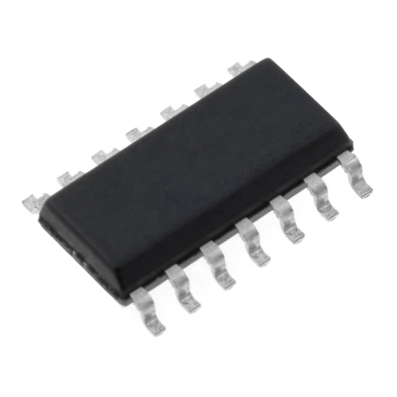
Page 31: External Dimensions / Marking Layout
RX - 8025 SA 9. External Dimensions / Marking Layout 9.1. External Dimensions RX-8025 SA (SOP-14pin) • External dimensions • Recommended soldering ± 10.1 0° - 10° ± 5.0 7.4 0.15 1.27 0.05 1.27 × 6 = 7.62 ± Min. 0.35 1.27 Unit : mm... -
Page 32: Reference Data
RX - 8025 SA 10. Reference Data (1) Example of frequency and temperature characteristics [Finding the frequency stability] θ = +25 °C Typ. × 10 α = -0.035 × 10 Typ. 1. Frequency and temperature characteristics can be approximated using the following equations. ∆f = α... -
Page 33: Application Notes
RX - 8025 SA 11. Application notes 1) Notes on handling This module uses a C-MOS IC to realize low power consumption. Carefully note the following cautions when handling. (1) Static electricity While this module has built-in circuitry designed to protect it against electrostatic discharge, the chip could still be damaged by a large discharge of static electricity. - Page 34 Unit 715-723 7/F Trade Square, 681 Cheung Sha Wan Road, Kowloon, Hong Kong Phone: (86) 755-2699-3828 (Shenzhen Branch) Fax: (86) 755-2699-3838 (Shenzhen Branch) http://www.epson.com.hk EPSON TAIWAN TECHNOLOGY & TRADING LTD. 14F, No.7, Song Ren Road, Taipei 110 Phone: (886) 2-8786-6688 Fax: (886)2-8786-6660 http://www.epson.com.tw/ElectronicComponent EPSON SINGAPORE PTE.