Table of Contents
Advertisement
Quick Links
Advertisement
Table of Contents

Related Manuals for Epson RX-4803SA/LC


Summary of Contents for Epson RX-4803SA/LC
- Page 1 ETM33E-04 Application Manua Real Time Clock Module RX-4803SA/LC Preliminary...
- Page 2 The information about applied circuitry, software, usage, etc. written in this material is intended for reference only. Seiko Epson does not assume any liability for the occurrence of infringing on any patent or copyright of a third party. This material does not authorize the licensing for any patent or intellectual copyrights.
-
Page 3: Table Of Contents
RX - 4803 SA / LC Contents 1. Overview........................1 2. Block Diagram ....................... 1 3. Terminal description ...................... 2 3.1. Terminal connections ......................... 2 3.2. Pin Functions ..........................2 4. Absolute Maximum Ratings ................... 3 5. Recommended Operating Conditions ................3 6. -
Page 4: Overview
RX - 4803 SA / LC Serial Interface Real-time Clock Module RX - 4803 SA / LC • Features built-in 32.768 kHz DTCXO, High Stability. • Serial interface in 4 lines form • Alarm interrupt function for day, date, hour, and minute settings •... -
Page 5: Terminal Description
RX - 4803 SA / LC 3. Terminal description 3.1. Terminal connections RX − 4803 SA RX − 4803 LC 1. CE 14. D I 1. N.C. 12. EVIN 2. CLK 13. DO 2. FOE 11. / INT 3. FOUT 12. -
Page 6: Absolute Maximum Ratings
RX - 4803 SA / LC 4. Absolute Maximum Ratings GND = 0 V Item Symbol Condition Rating Unit −0.3 to +6.5 Supply voltage Between V and GND −0.3 to +6.5 Input voltage CE, CLK, DI, FOE, EVIN pin Output voltage (1) DO, FOUT pin GND−0.3 to V +0.3... -
Page 7: Electrical Characteristics
RX - 4803 SA / LC 7. Electrical Characteristics 7.1. DC characteristics = 1.6 V to 5.5 V , Ta = −40 °C to +85 °C *Unless otherwise specified, GND = 0 V , V Item Symbol Condition Min. Typ. Max. -
Page 8: Ac Characteristics
RX - 4803 SA / LC 7.2. AC Characteristics * Unless otherwise specified, GND = 0 V , Ta = −40 °C to +85 °C 2.4V ≤ V < 4.5V 4.5V ≤ V ≤ 5.5V Item Symbol Condition Unit Min. Max. -
Page 9: Use Methods
RX - 4803 SA / LC 8. Use Methods 8.1. Description of Registers 8.1.1. Write / Read and Bank Select R/W and Register bank are specified by the four bits mode setting code. … Bank1: Basic time and calendar register Bank1 is compatible with RX-4801. -
Page 10: Register Table (Bank2)
RX - 4803 SA / LC 8.1.3. Register table (Bank2) Address Function bit 7 bit 6 bit 5 bit 4 bit 3 bit 2 bit 1 bit 0 Read Write 1/100 S HOUR WEEK ... -
Page 11: Details Of Registers
RX - 4803 SA / LC 8.2. Details of Registers It explains each register based on Bank2. 8.2.1. Clock counter ( 1/100S, SEC - HOUR ) Address Function bit 7 bit 6 bit 5 bit 4 bit 3 bit 2 bit 1 bit 0 1/100 S... -
Page 12: Calendar Counter ( Week - Year )
RX - 4803 SA / LC 8.2.2. Calendar counter ( WEEK - YEAR ) Address Function bit 7 bit 6 bit 5 bit 4 bit 3 bit 2 bit 1 bit 0 WEEK ∗) "o" indicates write-protected bits. A zero is always read from these bits. 1) Day of the WEEK counter •... -
Page 13: Alarm Registers
RX - 4803 SA / LC 8.2.3. Alarm registers Address Function bit 7 bit 6 bit 5 bit 4 bit 3 bit 2 bit 1 bit 0 MIN Alarm • HOUR Alarm WEEK Alarm • DAY Alarm • The alarm interrupt function is used, along with the AEI, AF, and WADA bits, to set alarms for specified date, day, hour, and minute values. -
Page 14: Flag Register
RX - 4803 SA / LC 5) FSEL0,1 ( FOUT frequency Select 0, 1 ) bits The combination of these two bits is used to set the FOUT frequency. FSEL1 FSEL0 FSEL0,1 FOUT frequency (bit 3) (bit 2) ∗ Default 32768 Hz Output 1024 Hz Output Write/Read... -
Page 15: Control Register
RX - 4803 SA / LC Data Description The VLF bit is cleared to zero to prepare for the next status detection. Write This bit is invalid after a "1" has been written to it. Data loss is not detected. Read Data loss is detected. - Page 16 RX - 4803 SA / LC Data Function When a time update interrupt event occurs, an interrupt signal is not generated or is canceled (/INT status changes from low to Hi-Z). When a time update interrupt event occurs, an interrupt signal is generated Write/Read (/INT status changes from Hi-Z to low).
-
Page 17: Osc Offset Contorol ( Reg -C / Bank 3 )
RX - 4803 SA / LC 8.2.8. OSC Offset Contorol ( Reg -C / Bank 3 ) Address Function bit 7 bit 6 bit 5 bit 4 bit 3 bit 2 bit 1 bit 0 OSC Offset ... -
Page 18: Capture Buffer / Event Control ( Bank 3 )
RX - 4803 SA / LC 8.2.9. Capture Buffer / Event control ( Bank 3 ) Address Function bit 7 bit 6 bit 5 bit 4 bit 3 bit 2 bit 1 bit 0 1/100 S CP SEC CP Event Control ... -
Page 19: Fixed-Cycle Timer Interrupt Function
RX - 4803 SA / LC 8.3. Fixed-cycle Timer Interrupt Function The fixed-cycle timer interrupt generation function generates an interrupt event periodically at any fixed cycle set between 244.14 µs and 4095 minutes. When an interrupt event is generated, the /INT pin goes to low level and "1" is set to the TF bit to report that an event has occurred. -
Page 20: Related Registers For Function Of Time Update Interrupts
RX - 4803 SA / LC 8.3.2. Related registers for function of time update interrupts. Address Function bit 7 bit 6 bit 5 bit 4 bit 3 bit 2 bit 1 bit 0 Timer Counter 0 • • • • Timer Counter 1 2048 1024... -
Page 21: Fixed-Cycle Timer Interrupt Interval (Example)
RX - 4803 SA / LC 5) TIE (Timer Interrupt Enable) bit When a fixed-cycle timer interrupt event occurs (when the TF bit value changes from "0" to "1"), this bit's value specifies whether an interrupt signal is generated (/INT status changes from Hi-Z to low) or is not generated (/INT status remains Hi-Z). -
Page 22: Time Update Interrupt Function
RX - 4803 SA / LC 8.4. Time Update Interrupt Function The time update interrupt function generates interrupt events at one-second or one-minute intervals, according to the timing of the internal clock. When an interrupt event occurs, the UF bit value becomes "1" and the /INT pin goes to low level to indicate that an event has occurred. -
Page 23: Related Registers For Time Update Interrupt Functions
RX - 4803 SA / LC 8.4.2. Related registers for time update interrupt functions. Address Function bit 7 bit 6 bit 5 bit 4 bit 3 bit 2 bit 1 bit 0 Extension Register USEL TEST WADA FSEL1 FSEL0 TSEL1 TSEL0 Flag Register ... -
Page 24: Alarm Interrupt Function
RX - 4803 SA / LC 8.5. Alarm Interrupt Function The alarm interrupt generation function generates interrupt events for alarm settings such as date, day, hour, and minute settings. When an interrupt event occurs, the AF bit value is set to "1" and the /INT pin goes to low level to indicate that an event has occurred. -
Page 25: Related Registers
RX - 4803 SA / LC 8.5.2. Related registers Address Function bit 7 bit 6 bit 5 bit 4 bit 3 bit 2 bit 1 bit 0 HOUR WEEK MIN Alarm • HOUR Alarm WEEK Alarm •... -
Page 26: Examples Of Alarm Settings
RX - 4803 SA / LC 3) AF (Alarm Flag) bit When this flag bit value is already set to "0", occurrence of an alarm interrupt event changes it to "1". When this flag bit value is "1", its value is retained until a "0" is written to it. Data Description The AF bit is cleared to zero to prepare for the next status detection... -
Page 27: Read/Write Of Data
RX - 4803 SA / LC 8.6. Read/Write of data For both read and write, first set up chip condition (internally CE="H") to CE="H" , then specify the 4-bits address, and finally read or write in 8-bits units. Both read and write use MSB-first. In continuous operation, objected address is auto incremented. -
Page 28: Vdd And Ce Timing
RX - 4803 SA / LC 8.7. V and CE timing * When the power is turned to ON, use with CE = " L " ( V [V] in the diagram ) as illustrated in the following timing chart. 1.6 V Item Symbol... -
Page 29: Connection With Typical Microcontroller
RX - 4803 SA / LC 8.9. Connection with Typical Microcontroller 4.7 µF Note Schottky Barrier Diode RX-4803 0.1 µF / INT FOUT Note : When using the seconding battery, the diode is not required. When using the primary battery, the diode is required. For detailed value on the resistance, please consult a battery maker. -
Page 30: Note About Read-Out Method Of A 1/100S Register
RX - 4803 SA / LC 8.11. Note about read-out method of a 1/100s register RA-4803 is equipped with a 1/100s register. As for 1/100 counters, it is worked in very fast clock than second. Therefore, as for the count operation of each, behavior in a chip access hold facility (P.8 reference) operation is different. When using a 1/100s register, be careful as follows. -
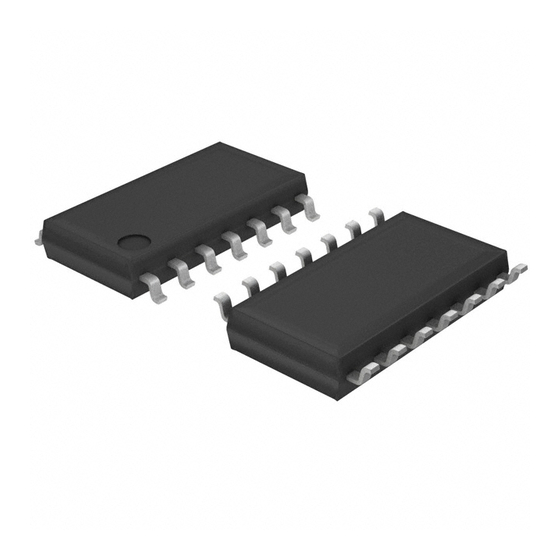
Page 31: External Dimensions / Marking Layout
RX - 4803 SA / LC 9. External Dimensions / Marking Layout 9.1. RX − 4803 SA 9.1.1. External dimensions RX − 4803 SA ( SOP − 14pin ) • External dimensions • Recommended soldering pattern ± 10.1 0° - 10° ±... - Page 32 RX - 4803 SA / LC 9.2. RX − 4803 LC 9.2.1. External dimensions RX − 4803 LC ( VSOJ − 20pin ) • External dimensions • Recommended soldering pattern ± 0.2 # 12 0.27 2.77 0.08 M 0.22 Unit : mm 0.08 ∗...
-
Page 33: Application Notes
RX - 4803 SA / LC 10. Application notes 1) Notes on handling This module uses a C-MOS IC to realize low power consumption. Carefully note the following cautions when handling. (1) Static electricity While this module has built-in circuitry designed to protect it against electrostatic discharge, the chip could still be damaged by a large discharge of static electricity. - Page 34 Unit 715-723 7/F Trade Square, 681 Cheung Sha Wan Road, Kowloon, Hong Kong Phone: (86) 755-2699-3828 (Shenzhen Branch) Fax: (86) 755-2699-3838 (Shenzhen Branch) http://www.epson.com.hk EPSON TAIWAN TECHNOLOGY & TRADING LTD. 14F, No.7, Song Ren Road, Taipei 110 Phone: (886) 2-8786-6688 Fax: (886)2-8786-6660 http://www.epson.com.tw/ElectronicComponent EPSON SINGAPORE PTE.