
Related Manuals for Sony HDVF-C35W


Summary of Contents for Sony HDVF-C35W
- Page 1 HD ELECTRONIC VIEWFINDER HDVF-C35W MAINTENANCE MANUAL 1st Edition Serial No. 100001 and Higher: HDVF-C35W (SY)
- Page 2 Ce manual est destiné uniquement aux personnes compétentes en charge de l’entretien. Afin de réduire les risques de décharge électrique, d’incendie ou de blessure n’effectuer que les réparations indiquées dans le mode d’emploi à moins d’être qualifié pour en effectuer d’autres. Pour toute réparation faire appel à une personne compétente uniquement. HDVF-C35W...
-
Page 3: Table Of Contents
1-10. Unleaded Solder ............. 1-10 (E) SW-1366 ............... 7-12 Frame Wiring ..............7-12 2. Setting Menu 2-1. Setting Menu ............2-1 (E) 2-2. TOP Menu ............... 2-2 (E) 2-3. OPERATION Menu ..........2-3 (E) 2-4. SERVICE Menu ............2-3 (E) 1 (E) HDVF-C35W... - Page 4 8. Board Layouts LE-341 ................8-1 LE-342 ................8-1 PR-308 ................8-2 PR-309 ................8-3 RE-249 ................8-4 SW-1366 ................. 8-4 2 (E) HDVF-C35W...
-
Page 5: Manual Structure
Manual Structure Purpose of this manual This manual is the maintenance manual of HD Electronic Viewfinder HDVF-C35W. This manual describes the information items on maintenance, and items that premise the service based on the components parts such as service overview, setting... -
Page 7: Service Overview
The PR-309 board consists of an AD converter, FPGA, image processing block, and clock generator. AD converter (IC1: I C control) The analog HD YPbPr signal supplied from the PR-308 board is digitally converted by ten bits and supplied to FPGA (IC100). 1-1 (E) HDVF-C35W... -
Page 8: Board
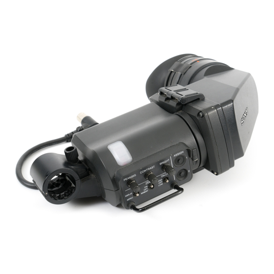
“MENU” and “ENTER” switches at the bottom is sent to CPU (IC400) on the PR-308 board. 1-2-4. SW-1366 Board “PEAKING”, “CONTRAST”, and “BRIGHT” volume values, and “ASSIGN.1” and “ASSIGN.2” switch ON/ OFF signals are sent through the RE-249 board to CPU (IC400) on the RP-308 board. 1-2 (E) HDVF-C35W... -
Page 9: Input And Output Signals Of Connectors
All OFF (bit1 to 4: OFF) S401 bit1 to 4, 6 Not used All OFF bit5 SOFT DEBUG Normal OFF: DEBUG bit7 BOOT SOFT VERSION UP Version upgrade OFF: Normal bit8 MAIN SOFT VERSION UP Version upgrade OFF: Normal 1-3 (E) HDVF-C35W... -
Page 10: Replacing The Main Parts
LCD module. LE-341 board LE-342 board Harness Ground terminal 3. Remove the three screws, then remove the stopper. 4. Open LCD in the direction of the arrow. B2 x 5 Stopper Harnesses CN102 B2 x 5 LCD module 1-4 (E) HDVF-C35W... -
Page 11: How To Measure Luminance
1. Remove the elbow assenbly. (Refer to steps 1 and 2 of Section 1-5-1.) Spacer sheet 2. Attach the front chassis of the HDVF-C35W in the camera. 3. Rotate the BRIGHT knob and CONTR knob fully 12. Attach the LCD module in the reverse order of steps 1 clockwise (MAX) beforehand. -
Page 12: Procedure Required When Replacing The Pr-308 Board And Ic406
(B) and drip-proof cushion from the connecting cord (VF). Adjustment equipment Connecting cord (VF) Cable retaining plate (B) Adjustment equipment Model name Display color analyzer KONICA MINOLTA sensing CA-210 or equivalent Cable retaining plate (A) Drip-proof cushion 1-6 (E) HDVF-C35W... -
Page 13: Procedure For Extending The Re-249 Board
7. Remove the connecting cord (VF) from the lower case B2 x 4 B2 x 4 assembly. PR-309 board B2 x 4 B2.6 x 5 Ground terminal PR-308 board Ground terminal Connecting cord (VF) Harness guide Lower case assembly B2.6 x 8 1-7 (E) HDVF-C35W... -
Page 14: Firmware And Software
2. Display the “08 VERSION” screen in the SERVICE B2 x 4 menu. (Refer to Section 2-4.) Ground terminals VF MENU S08 VERSION RE-249 board SOFTWARE MAIN: 1.00-00 BOOT: 1.00-00 FPGA : 1.00-0 Lower case assembly 3. Check the ROM version. 1-8 (E) HDVF-C35W... -
Page 15: Writing And Rewriting Pld Internal Data
2. Standard software (PLD Download Tool) can be used. Step 2. With the power of the device turned off, connect . The PLD internal data is managed on the Sony database the parallel port on the PC and the EPR connector server as a Project file (E_xxx_xxx_xx_xx). -
Page 16: Recommended Replacement Parts
LCD burnout. The viewfinder lens has taken special measures to prevent LCD burnout. LCD burnout due to the condensed sunlight caused by the use of other viewfinder lens is not covered by the warranty. 1-10 (E) HDVF-C35W... -
Page 17: Setting Menu
MENU switch to return to Returning to previous page, shifting of item and item select mode. Push the MENU switch again to decreasing of setting value are performed. return to page select mode. 2-1 (E) HDVF-C35W... -
Page 18: Top Menu
2 switch to decrease the value. SERVICE Contains items required for maintaining the Keep pushing the switch to change the value rapidly. View Finder, such as electrical alignment, HOURS METER, and self-diagnosis function. 2-2 (E) HDVF-C35W... -
Page 19: Operation Menu
SKIN, SKY, FOIL, ORAN and B ch when mixing the peaking signal to the main signal. This setting is enabled only when RGB is selected in SOURCE. [0] to 63 CRISPENING Sets the level for crispening the peaking signal. 2-3 (E) HDVF-C35W... - Page 20 In this case, a dedicated VF connection cable and the corresponding camera settings are needed. Contact your nearest SONY Office/Service Center for details. No setting change is required when connecting the device to the EXT I/O (20P) connector of HDC-F950.
- Page 21 *6 : Place the cursor mark “→” on “EXEC” and press the ENTER switch to move to the following operation screen. Place the cursor mark “→” on “YES” and press the ENTER switch to perform reset. VF MENU S09 RESET RESET OK? MENU RESET EXEC 2-5 (E) HDVF-C35W...
-
Page 23: Electrical Alignment
3-1-1. Description of Switches, Controls, . HDVS camera and Menu Settings HDC1500, HDW-F900R, or equivalent . AC adapter Sony AC-DN10 or equivalent Configure the following settings for the switch, control, and menu settings for making adjustments in this section 3-1-3. Connection unless otherwise directed. -
Page 24: Color Temperature Check
(2) Measure the color temperature of the center area of screen. Measurement instrument: Display color analyzer Measuring point: Center area of screen x = 0.283 ± 0.005 Spec: y = 0.298 ± 0.008 (3) Check that the specification is satisfied. 3-2 (E) HDVF-C35W... -
Page 25: Spare Parts
Therefore, specified parts should be used in the case of replacement. 2. Standardization of Parts Some repair parts supplied by Sony differ from those used for the unit. These are because of parts common- ality and improvement. 3. Stock of Parts Parts marked with “o”... -
Page 26: Exploded Views
7-627-554-18 s SCREW,PRECISION +P 2X3.5 TYPE1 1-965-435-11 s HARNESS, SUB (LE-U/L) 1-965-439-11 s HARNESS, SUB (LCD) 3-364-941-01 s SCREW(+B)(2.6X5),NYLOK 1-965-562-11 s HARNESS, SUB (GND) 2-277-457-01 s KNOB, STOPPER 2-277-466-01 s SPRING, COMPRESSION 7-621-775-40 s SCREW +B 2.6X8 7-624-102-04 s STOP RING 1.5, TYPE -E HDVF-C35W... - Page 27 3-209-282-01 s CUSHION, WATER PROTECT 7-621-734-09 s SET-SCT,HEX. 2.6X3 7-621-775-40 s SCREW +B 2.6X8 3-209-283-01 s SPACER SHEET 7-624-102-04 s STOP RING 1.5, TYPE -E 3-209-284-01 s CUSHION REAR 3-209-305-02 s RING, ROTATION 3-209-316-01 s PIN, SLIDE 3-209-407-01 s HINGE HDVF-C35W...
- Page 28 1-788-641-11 s LOUPE, VF 3-209-273-01 s MIRROR 3-209-278-02 s PLATE, DISPLAY 3-209-286-01 s FILTER, CC 3-209-288-01 s EYE CUP 3-209-291-01 s RING,FIX 3-209-408-01 s SHEET,GRIP 3-209-823-01 s SEAL,PROTECT 3-602-979-02 s LABEL,CAUTION 3-692-547-01 o PIN, PARALLEL 3-692-547-11 o PIN, PARALLEL HDVF-C35W...
-
Page 29: Electrical Parts List
C315 1-165-870-21 s CAP, ELECT 100MF (6.3X6) C400 1-100-916-11 s CAP, CERAMIC 0.1MF X7R 1005 C401 1-100-916-11 s CAP, CERAMIC 0.1MF X7R 1005 C402 1-114-130-11 s CAP, CERAMIC 1MF X6S 1005 C403 1-114-130-11 s CAP, CERAMIC 1MF X6S 1005 HDVF-C35W... - Page 30 C607 1-112-691-11 s CAP, CERAMIC 22MF R 3225 IC402 8-759-672-76 s IC AK9813BF-E2 C608 1-100-916-11 s CAP, CERAMIC 0.1MF X7R 1005 IC403 6-704-832-01 s IC IS61LV6416-10TLT C609 1-112-691-11 s CAP, CERAMIC 22MF R 3225 IC404 8-759-592-47 s IC TC7SZ08FU(TE85R) HDVF-C35W...
- Page 31 1-218-990-81 s CONDUCTOR, CHIP (1005) R409 1-208-935-81 s RES, CHIP 100K (1005) R110 1-218-990-81 s CONDUCTOR, CHIP (1005) R410 1-208-935-81 s RES, CHIP 100K (1005) R111 1-218-941-11 s RES, CHIP 100 (1005) R411 1-208-699-11 s RES, CHIP 4.7K (1005) HDVF-C35W...
- Page 32 1-208-683-11 s RES, CHIP 1.0K (1005) R602 1-208-683-11 s RES, CHIP 1.0K (1005) R477 1-208-683-11 s RES, CHIP 1.0K (1005) R603 *a 1-208-935-81 s RES, CHIP 100K (1005) R478 1-208-911-81 s RES, CHIP 10K (1005) R604 *a 1-208-935-81 s RES, CHIP 100K (1005) HDVF-C35W...
- Page 33 C110 1-100-916-11 s CAP, CERAMIC 0.1MF X7R 1005 TP300 1-535-877-22 s CHIP, CHECKER C111 1-100-916-11 s CAP, CERAMIC 0.1MF X7R 1005 TP400 1-535-877-22 s CHIP, CHECKER C112 1-100-916-11 s CAP, CERAMIC 0.1MF X7R 1005 TP401 1-535-877-22 s CHIP, CHECKER HDVF-C35W...
- Page 34 1-100-916-11 s CAP, CERAMIC 0.1MF X7R 1005 C207 1-100-916-11 s CAP, CERAMIC 0.1MF X7R 1005 C300 1-100-916-11 s CAP, CERAMIC 0.1MF X7R 1005 C208 1-100-916-11 s CAP, CERAMIC 0.1MF X7R 1005 C301 1-100-916-11 s CAP, CERAMIC 0.1MF X7R 1005 4-10 HDVF-C35W...
- Page 35 *a 1-218-990-81 s CONDUCTOR, CHIP (1005) IC104 8-759-679-55 s IC SN74LVC08APWR R100 1-208-855-81 s RES, CHIP 47 (1005) R101 1-208-855-81 s RES, CHIP 47 (1005) IC105 8-759-592-47 s IC TC7SZ08FU(TE85R) R102 1-218-941-11 s RES, CHIP 100 (1005) IC106 8-759-330-14 s IC TL7700CPS-E20 4-11 HDVF-C35W...
- Page 36 1-208-911-81 s RES, CHIP 10K (1005) R901 1-218-990-81 s CONDUCTOR, CHIP (1005) R172 1-218-990-81 s CONDUCTOR, CHIP (1005) R902 1-218-941-11 s RES, CHIP 100 (1005) R173 1-218-990-81 s CONDUCTOR, CHIP (1005) R903 1-218-941-11 s RES, CHIP 100 (1005) 4-12 HDVF-C35W...
- Page 37 1-234-371-21 s RES, NETWORK 47 (1005X4) RB312 1-234-371-21 s RES, NETWORK 47 (1005X4) RB313 1-234-371-21 s RES, NETWORK 47 (1005X4) RB314 1-234-371-21 s RES, NETWORK 47 (1005X4) RB315 1-234-371-21 s RES, NETWORK 47 (1005X4) 1-535-877-22 s CHIP, CHECKER 4-13 HDVF-C35W...
- Page 38 1-112-046-11 s CAP, CERAMIC 4.7MF X6S 2012 1-400-868-11 s COIL, CHOKE 22UH 1-400-869-11 s COIL, CHOKE 47UH 1-125-827-91 s CAP, CHIP CERAMIC 1MF B 1-456-622-21 s COIL, CHOKE 1UH 1-164-882-81 s CAP,CHIP CERAMIC 220PF CH 1005 1-456-622-21 s COIL, CHOKE 1UH 4-14 HDVF-C35W...
- Page 39 1-208-911-81 s RES, CHIP 10K (1005) 1-208-915-81 s RES, CHIP 15K (1005) 1-208-887-81 s RES, CHIP 1.0K (1005) 1-208-919-81 s RES, CHIP 22K (1005) 1-208-919-81 s RES, CHIP 22K (1005) 1-208-927-81 s RES, CHIP 47K (1005) 1-208-883-81 s RES, CHIP 680 (1005) 4-15 HDVF-C35W...
-
Page 40: Packing Materials & Supplied Accessories
1-762-489-11 s SWITCH, TOGGLE 1-762-400-21 s SWITCH 1-762-400-21 s SWITCH THP1 1-802-063-21 s THERMISTOR, POSITIVE 1-535-877-22 s CHIP, CHECKER 1-535-877-22 s CHIP, CHECKER 1-535-877-22 s CHIP, CHECKER 1-535-877-22 s CHIP, CHECKER 1-535-877-22 s CHIP, CHECKER 1-535-877-22 s CHIP, CHECKER 4-16 HDVF-C35W... - Page 41 In addition, for semiconductors with ID Nos., refer to the separate CD-ROM titled “Semiconductor Pin Assignments” (Sony Part No. 9-968-546-06) that allows searching for parts by semiconductor type or ID No. The semiconductors in the manual or on the CD-ROM are listed by equivalent types.
-
Page 43: Block Diagrams
+3.3V : ANA/ADC/SCALER/FPGA/SDRAM/uCOM _ 3.3V SWITCHING _ 3.3V : LCD/FPGA CONVERTER +1.8V : SCALER/FPGA/ADC DC/DC +1.5V : FPGA Q25, L7 CONTOROL Q5, Q6 _3.3V : ANA + 1.5V SWITCHING CONVERTER SHUNT OP AMP DOWN H_SHUTDOWN DETECT RE-249 (1/2) Overall HDVF-C35W... - Page 45 UDZSTE-175.6B LE-341 BOARD NO. 1-873-971-11 0.1uF FA1112H-TR D/L1_TALLY(!) AMBER D/L2_TALLY(MAG) D/C_TALLY(RED) D/R1_TALLY(3RD) D/R2_TALLY MIRROR_SW FY1111C-634-TR 10 9 YELLOW UDZSTE-175.6B UDZSTE-175.6B UDZSTE-175.6B UDZSTE-175.6B UDZSTE-175.6B UDZSTE-175.6B UDZSTE-175.6B FR1112H-TR R_TALLY FY1111C-634-TR YELLOW X_TALLY FA1112H-TR AMBER SAVE MIRROR_SW LE-342 BOARD NO. 1-873-972-11, 12 HDVF-C35W...
- Page 46 0.1uF 6.3V VSOUT V_SYNC(SEP) GND_ANA CL6 0.8 VFOUT GND_ANA GND_ANA CSOUT BPOUT 0.1uF 0.1uF REXT OEOUT O/E_FIELD(SEP) AD8061ARTZ-REEL7 0.1uF GND_ANA GND_ANA GND_ANA 0.1uF 10pF 10pF GND_ANA GND_ANA GND_ANA GND_ANA GND_ANA PR-308 (1/3) 0.1uF Comp/Video BOARD NO. 1-873-969-11, 12 GND_ANA HDVF-C35W...
- Page 47 ENABLE READY R424 100k Mount to A side Mount to B side R425 100k IC409 R426 100k FRONT_TALLY_ENBL CAT24C16WI-GT3 IC408 R427 100k LTC4300A-1IMS8#TR R428 100k C421 PR-308 (2/3) For ROM ICE R431 100 CL601-607 BOARD NO. 1-873-969-11, 12 Comp/Video HDVF-C35W...
- Page 48 FPGA_SCL_I2C R610 0 R627 0 FPGA_SDA(3.3V) FPGA_SDA_I2C R611 0 R628 0 SUFFIX -12 C611 C612 R633 R612 0 R629 0 R621 0.1uF 0.1uF 34 33 32 31 PR-308 (3/3) R617 R630 IC602 IC603 BOARD NO. 1-873-969-11, 12 TC74HC4053AFT(EL) TC74HC4053AFT(EL) HDVF-C35W...
- Page 49 2.5V 0.1uF Mount to A side Mount to B side 2.2uH 0.1uF 82nF 0.1uF 0.1uF A_GND 0.1uF 470uF 0.1uF 2.5V 0.01uF 0.01uF A_GND A_GND A_GND Mount to B side A/D_PCLK 28.63636MHz 11pF 11pF PR-309 (1/5) BOARD NO. 1-873-970-11, 12 HDVF-C35W...
- Page 50 IN2_D[17] 10uF EPR2_DCLK 0.1uF EPR2_CONFIG_DONE PI2_D[18] IN2_D[18] EPR2_CONFIG_DONE CL48 CL161 R172 PI2_D[19] IN2_D[19] CL167 CL125 EPR2_nCONFIG CL151 CL166 CL164 2ndInput_iChips 001,003 near IC100 CL163 CL165 R179 CL162 EPR2_nCS CS_FPGA PR-309 (2/5) CPU_INT BOARD NO. 1-873-970-11, 12 CPU_CLOCK OSD_G_FPGA OSD_R_FPGA HDVF-C35W...
- Page 51 USIN[B6] R210 GND58[T17] POHS UCMD0[A5] GND57[U17] POVS UCMD1[B5] GND56[U16] +3.3V_iChips POACT +3.3V_iChips R203 R211 R212 R201 R206 R208 <- POCLK_33.2M R213 R209 SUFFIX -12 CS_IP 002,005 SPI_STD R227 002,005 SPI_SRD SPI_SCLK R226 SPI_SCLK_BUF PR-309 (3/5) BOARD NO. 1-873-970-11, 12 HDVF-C35W...
- Page 52 MEM0_DQM3 MDQM3[AC3] MEM1_DQM0 MDQM4[AD7] MEM1_DQM1 MDQM5[AE7] equal length MEM1_DQM2 near IC200 MDQM6[AD8] MEM1_DQM3 MDQM7[AF8] MCLK1 R310 10 <- MCLKO1 MCLKO1[T3] PR-309 (4/5) MCLK2 R311 10 MCLKO2 <- MCLKO2[AE8] 77MHz*1.875 BOARD NO. 1-873-970-11, 12 equal length =144.375MHz IC200 (3/3) IP00C760 HDVF-C35W...
- Page 53 SUFFIX -12 SPI_SRD 002,003,005 SDA(3.3V) 3.3V_SDA_I2C 001,002 SCK(3.3V) 3.3V_SCL_I2C 001,002 H SYNC(SEP) H_SYNC_SEP +3.3V C400 JC401 V SYNC(SEP) V_SYNC_SEP 0.1uF O/E(SEP) O/E_FIELD_SEP CPU_RESET CPU_RESET CPU_CLOCK CPU_CLOCK OUTY IC400 TC7SZ125FU(TE85R) 34 33 32 31 PR-309 (5/5) BOARD NO. 1-873-970-11, 12 HDVF-C35W...
- Page 54 INV2 UDZSTE-172.7B 6.3V 150uF 10uF 10uF 6.3V 6.3V MBR0530T1 10uF 10uH 0.022uF (17/61) CN1 +1.8V(IP) 1.0A (18/61) CN1 +1.8V(IP) SI4804BDY-T1 (29/61) CN1 DTC114TE-TL +1.8V(A/D) 0.0068uF +1.8V (30/61) CN1 +1.8V(A/D) R127 R126 H_START_UP DTC114TE-TL DTC114TE-TL DTC114TE-TL (37/61) (38/61) 7-10 7-10 HDVF-C35W...
- Page 55 UDZSTE-173.6B (50/61) N.C. (51/61) N.C. R115 HIGH UDZSTE-173.6B (46/61) CN1 UP_TALLY_-H TALLY (47/61) CN1 UP_TALLY_-L (61/61) R116 1000pF 1000pF UDZSTE-173.6B R117 MENU (48/61) CN1 MENU (49/61) CN1 1000pF R118 UDZSTE-173.6B 1000pF RE-249 UDZSTE-173.6B BOARD NO. 1-873-968-11, 12 7-11 7-11 HDVF-C35W...
-
Page 56: Frame Wiring
SUFFIX: -11 LCD BLOCK LCD PANEL PR-309 CN102 +3.3V PEAKING CONTRAST BRIGHT IF-1070 0.1uF 22uF +3.3V PEAKING CONTRAST BRIGHT ASSIGN.1 ASSIGN.2 ASSIGN.1 CN600 CN601 UDZSTE-173.6B ASSIGN.2 UDZSTE-173.6B LE-341 SW-1366 BOARD NO. 1-873-973-11 LE-342 PR-308 RE-249 SW-1366 Frame Wiring 7-12 7-12 HDVF-C35W... - Page 57 PR-308 PR-309 RE-249 SW-1366 LE-341 -A SIDE- SUFFIX: -11 LE-342 -A SIDE- SUFFIX: -11, -12 LE-341 -B SIDE- SUFFIX: -11 LE-342 -B SIDE- SUFFIX: -11, -12 --------------------- -------------------------- LE-341 (1-873-971-11) LE-342 (1-873-972-11, -12) --------------------- -------------------------- *:B SIDE *:B SIDE HDVF-C35W...
- Page 58 R494 RB410 *B1 C414 R404 R495 RB411 *B1 SUFFIX: -11, -12 C415 R405 R496 RB412 *B1 C416 R406 R497 RB413 *B1 C417 CN400 R407 R498 RB414 *B1 C418 CN600 R408 R499 RB415 *B1 C419 CN601 R409 R500 RB416 *B1 HDVF-C35W...
- Page 59 R203 RB238 C136 C264 R110 R204 RB300 C137 C265 R111 R205 RB301 PR-309 -B SIDE- C138 C300 R112 R206 RB302 C139 C301 R113 R207 RB303 SUFFIX: -11, -12 C140 C302 R116 R208 RB304 C141 C303 D100 R117 R209 RB305 HDVF-C35W...
- Page 60 SUFFIX: -11, -12 SW-1366 -B SIDE- SUFFIX: -11 R100 R101 R102 R103 R104 R105 R106 R107 R108 R109 R111 R112 R113 R114 R115 R116 R117 R118 R119 R120 R126 RE-249 R127 -B SIDE- R128 R129 SUFFIX: -11, -12 R130 R131 HDVF-C35W...
- Page 62 Printed in Japan Sony Corporation HDVF-C35W (SY) J, E 2007. 6 22 9-968-349-01 ©2007...