Table of Contents
Advertisement
Quick Links
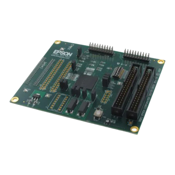
S1D13513 Display Controller
S5U13513P00C100 Evaluation Board
User Manual
Document Number: X78A-G-003-01
Status: Revision 1.1
Issue Date: 2010/09/06
© SEIKO EPSON CORPORATION 2006-2010. All Rights Reserved.
Information in this document is subject to change without notice. You may download and use this document, but only for your own use in
evaluating Seiko Epson/EPSON products. You may not modify the document. Epson Research and Development, Inc. disclaims any
representation that the contents of this document are accurate or current. The Programs/Technologies described in this document may contain
material protected under U.S. and/or International Patent laws.
EPSON is a registered trademark of Seiko Epson Corporation. All other trademarks are the property of their respective owners.
Revision 1.1
Advertisement
Table of Contents

Related Manuals for Epson S5U13513P00C100


Summary of Contents for Epson S5U13513P00C100
- Page 1 The Programs/Technologies described in this document may contain material protected under U.S. and/or International Patent laws. EPSON is a registered trademark of Seiko Epson Corporation. All other trademarks are the property of their respective owners. Revision 1.1...
- Page 2 Page 2 Epson Research and Development Vancouver Design Center S1D13513 S5U13513P00C100 Evaluation Board User Manual X78A-G-003-01 Issue Date: 2010/09/06 Revision 1.1...
-
Page 3: Table Of Contents
Schematic Diagrams ........24 S5U13513P00C100 Board Layout ......28 References . - Page 4 Page 4 Epson Research and Development Vancouver Design Center S1D13513 S5U13513P00C100 Evaluation Board User Manual X78A-G-003-01 Issue Date: 2010/09/06 Revision 1.1...
-
Page 5: Introduction
Adapter board so that it can be used with a laptop or desktop computer, via USB 2.0. With some minor modifications, it is possible to connect the S5U13513P00C100 evaluation board to a Epson PC Card Extender board instead of a USB Adapter board. The S5U13513P00C100 evaluation board can also be used with many other native platforms via the host connectors which provide the appropriate signals to support a variety of CPUs. -
Page 6: Features
Epson Research and Development Vancouver Design Center 2 Features The S5U13513P00C100 Evaluation Board includes the following features: • 256-pin PBGA S1D13513 Display Controller • On-board SDRAM, selectable as 8MB x 32-bit or 8MB x 16-bit • Headers for connection to the S5U13U00P00C100 USB Adapter board or to the PC Card Extender board •... -
Page 7: Installation And Configuration
Page 7 Vancouver Design Center 3 Installation and Configuration The S5U13513P00C100 evaluation board incorporates a DIP switch, jumpers, and 0 ohm resistors which allow it to be used with a variety of different configurations. 3.1 Configuration DIP Switch The S1D13513 has configuration inputs (CNF[8:0]) which are read on the rising edge of RESET#. - Page 8 Serial on HVDD2: Data valid on rising edge 11010b Reserved 11011b Reserved 11100b Reserved 11101b Reserved 11110b Reserved 11111b Reserved = Required settings when using S5U13U00P00C100 USB Adapter board (SW1-[9:1] = 101000000b) S1D13513 S5U13513P00C100 Evaluation Board User Manual X78A-G-003-01 Issue Date: 2010/09/06 Revision 1.1...
- Page 9 SH3 Big Endian: Active Low WAIT# with tri-state 11101b SH3 Big Endian: Active Low WAIT# always driven 11110b SH4 Big Endian: Active High WAIT# with tri-state 11111b Reserved S5U13513P00C100 Evaluation Board User Manual S1D13513 Issue Date: 2010/09/06 X78A-G-003-01 Revision 1.1...
-
Page 10: Configuration Jumpers
Page 10 Epson Research and Development Vancouver Design Center 3.2 Configuration Jumpers The S5U13513P00C100 has 11 jumper blocks which configure various board settings. The jumper positions for each function are shown below. Table 3-4: Configuration Jumper Summary Jumper Function Position 1-2... - Page 11 JP7 for HVDD2 (LCD Panel interface) JP8 for HVDD3 (Camera2 interface) JP9 for HVDD4 (Camera1 interface) JP10 for HVDD5 (SDRAM interface) JP10 Figure 3-2: Configuration Jumper Locations (JP1-JP10) S5U13513P00C100 Evaluation Board User Manual S1D13513 Issue Date: 2010/09/06 X78A-G-003-01 Revision 1.1...
- Page 12 When the jumper is at position 2-3, the external SDRAM is 16-bit wide and memory size is 16MB. In this position one memory chip is disabled and only one chip is active (16MB and 16-bit wide). JP11 Figure 3-3: Configuration Jumper Location (JP11) S1D13513 S5U13513P00C100 Evaluation Board User Manual X78A-G-003-01 Issue Date: 2010/09/06 Revision 1.1...
-
Page 13: Technical Description
The green LED ‘3.3V Power’ is turned on when 3.3V power is applied to the board. 4.1.2 Voltage Regulators The S5U13513P00C100 evaluation board has an on-board linear regulator to provide the 1.8V power required by the S1D13513 Display Controller. Additionally, there is a step-up switching voltage regulator to generate 6~24V. This output is adjustable and can be used to power the LED backlight on some LCD panels. -
Page 14: Clocks
For the S5U13513P00C100 evaluation board, OSC1 and OSC2 use crystals (10MHz for OSC1 and 27MHz for OSC2). For the S5U13513P00C100 evaluation board, CLKI3 is not used and is pulled to ground by a 10kΩ resistor. However, if CLKI3 is required, connect a 14-pin, DIP package oscillator in the Y1 footprint. -
Page 15: Host Interface
3. Plug the PC Card Extender (with S5U13513P00C100 connected to it) into a PC Card slot on a PC. 4. Turn on the 3.3V power supply and the S5U13513P00C100 is ready to use. Note that a windows driver is required to be installed on the PC (the S1D13xxx PCI/PC Card Bus driver is available from www.erd.epson.com). -
Page 16: Direct Host Bus Interface Support
All S1D13513 host interface pins are available on connectors H2 and H3 which allow the S5U13513P00C100 to be connected to a variety of development platforms. However, connectors H2 and H3 are not populated on the S5U13513P00C100 evaluation board. If connectors H2 and H3 are added, all host interface signals must match HVDD1 of the S1D13513. -
Page 17: Lcd Panel Interface
40mA current available from the on-board voltage regulator. The following diagram shows the location of the LCD panel connectors H4 and H5. Figure 4-2: LCD Panel Connectors Locations (H4, H5) S5U13513P00C100 Evaluation Board User Manual S1D13513 Issue Date: 2010/09/06 X78A-G-003-01... -
Page 18: Camera Interface
The reset signal provided on H6 and H7 is active low and is pulled to HIOVDD when inactive. The following diagram shows the location of the camera connectors H6 and H7. Figure 4-3: Camera Expansion Connector Locations (H6, H7) S1D13513 S5U13513P00C100 Evaluation Board User Manual X78A-G-003-01 Issue Date: 2010/09/06 Revision 1.1... -
Page 19: Yuv Output For Tv Display
The S1D13513 Display Controller GPIO pins have multiple functions. All the GPIO pins are routed to the connectors on the S5U13513P00C100 evaluation board. If any pin is configured as a GPIO, it will be available on the connectors as listed below: GPIOA[7:0] pins are routed to connector H7. -
Page 20: Jtag Connector
H1, however, connector H1 is not populated on the board. For the pinout of connector H1, see “Schematic Diagrams” on page 24. The following diagram shows the location of the JTAG connector (H1). Figure 4-4: JTAG Connector Location S1D13513 S5U13513P00C100 Evaluation Board User Manual X78A-G-003-01 Issue Date: 2010/09/06 Revision 1.1... -
Page 21: Parts List
FILTER 3-TERM 60MHZ F1, F2 ACF451832-222 TDK ACF451832-222 300MA SMD HEADER 6X2 Samtec TSW-106-05-G-D H2, H3 HEADER_17X2 AMP 1-87215-7 LCD Connector Samtec TST-120-01-G-D Extended LCD Connector Samtec TST-120-01-G-D S5U13513P00C100 Evaluation Board User Manual S1D13513 Issue Date: 2010/09/06 X78A-G-003-01 Revision 1.1... - Page 22 Panasonic - ECG EVN- R106 200k 5ESX50B25 SH1, SH2, SH3, SH4, Sullins Electronics Corp. SH5, SH6, SH7, SH8, .100 in. Jumper Shunt JUMPER SHORTING TIN STC02SYAN SH9, SH10, SH11 S1D13513 S5U13513P00C100 Evaluation Board User Manual X78A-G-003-01 Issue Date: 2010/09/06 Revision 1.1...
- Page 23 Texas Instruments TPS3801L30DCKR SOT-323-5 TPS3801L30DCKR Alternate MIC39100- MIC37100-1.8WS Micrel MIC37100-1.8WS 1.8WS IC CONV DC/DC BOOST TPS61040 TI TPS61040DVBR LP SOT-23-5 MA-506 10.0000M MA-506 27.0000M 14-Pin DIP AMP 2-641609-1 S5U13513P00C100 Evaluation Board User Manual S1D13513 Issue Date: 2010/09/06 X78A-G-003-01 Revision 1.1...
-
Page 24: Schematic Diagrams
Page 24 Epson Research and Development Vancouver Design Center 6 Schematic Diagrams Figure 6-1: S5U13513P00C100 Schematics (1 of 4) S1D13513 S5U13513P00C100 Evaluation Board User Manual X78A-G-003-01 Issue Date: 2010/09/06 Revision 1.1... - Page 25 2Mb x 16-bit x 4 2Mb x 16-bit x 4 2Mb x 16-bit x 4 2Mb x 16-bit x 4 banks banks banks banks Figure 6-2: S5U13513P00C100 Schematics (2 of 4) S5U13513P00C100 Evaluation Board User Manual S1D13513 Issue Date: 2010/09/06 X78A-G-003-01 Revision 1.1...
- Page 26 Page 26 Epson Research and Development Vancouver Design Center Figure 6-3: S5U13513P00C100 Schematics (3 of 4) S1D13513 S5U13513P00C100 Evaluation Board User Manual X78A-G-003-01 Issue Date: 2010/09/06 Revision 1.1...
- Page 27 Epson Research and Development Page 27 Vancouver Design Center Figure 6-4: S5U13513P00C100 Schematics (4 of 4) S5U13513P00C100 Evaluation Board User Manual S1D13513 Issue Date: 2010/09/06 X78A-G-003-01 Revision 1.1...
-
Page 28: S5U13513P00C100 Board Layout
Page 28 Epson Research and Development Vancouver Design Center 7 S5U13513P00C100 Board Layout Figure 7-1: S5U13513P00C100 Board Layout - Top View S1D13513 S5U13513P00C100 Evaluation Board User Manual X78A-G-003-01 Issue Date: 2010/09/06 Revision 1.1... - Page 29 Epson Research and Development Page 29 Vancouver Design Center Figure 7-2: S5U13513P00C100 Board Layout - Bottom View S5U13513P00C100 Evaluation Board User Manual S1D13513 Issue Date: 2010/09/06 X78A-G-003-01 Revision 1.1...
-
Page 30: References
Page 30 Epson Research and Development Vancouver Design Center 8 References 8.1 Documents • Epson Research and Development, Inc., S1D13513 Hardware Functional Specification, document number X78B-A-001-xx. 8.2 Document Sources • Epson Research and Development Website: http://www.erd.epson.com. S1D13513 S5U13513P00C100 Evaluation Board User Manual... -
Page 31: Technical Support
421-8, Hino, Hino-shi, Tokyo 191-8501, JAPAN Phone: +81-42-587-5814 FAX: +81-42-587-5117 9.2 Ordering Information To order the S5U13513P00C100 Evaluation Board, contact the Epson sales representative in your area and order part number S5U13513P00C100. S5U13513P00C100 Evaluation Board User Manual S1D13513 Issue Date: 2010/09/06 X78A-G-003-01 Revision 1.1... - Page 32 • added board layout X78A-G-003-00 Revision 0.02 • revised manual due to design changes • added new schematics • added new parts list X78A-G-003-00 Revision 0.01 • Initial draft of manual S1D13513 S5U13513P00C100 Evaluation Board User Manual X78A-G-003-01 Issue Date: 2010/09/06 Revision 1.1...