Table of Contents
Advertisement
Quick Links
IMPORTANT INFORMATION ABOUT LEAD FREE, (PbF), SOLDERING
If lead free solder was used in the manufacture of this product the printed circuit boards will be marked PbF.
Standard leaded, (Pb), solder can be used as usual on boards without the PbF mark.
When this mark does appear please read and follow the special instructions described in this manual on the use of PbF and how
it might be permissible to use Pb solder during service and repair work.
High Speed Laser Fax and Copier
KX-FL612CX
KX-FL612CX-S
(for Asia, Middle Near East and Africa)
(for Saudi Arabia )
© 2005 Panasonic Communications Co., Ltd. All
rights
reserved.
distribution is a violation of law.
ORDER NO. KMF0501841C3
Unauthorized
copying
and
Advertisement
Table of Contents
Troubleshooting

Related Manuals for Panasonic KX-FL612CX


Summary of Contents for Panasonic KX-FL612CX
- Page 1 When this mark does appear please read and follow the special instructions described in this manual on the use of PbF and how it might be permissible to use Pb solder during service and repair work. © 2005 Panasonic Communications Co., Ltd. All rights reserved.
-
Page 2: Table Of Contents
KX-FL612CX / KX-FL612CX-S CONTENTS Page Page 1 INTRODUCTION 5.20. HOW TO REMOVE THE FUSER UNIT 1.1. ABOUT LEAD FREE SOLDER (PbF: Pb free) 5.21. HOW TO REMOVE THE CIS 1.2. HOW TO RECOGNISE THAT Pb FREE SOLDER IS 5.22. NOTE FOR ASSEMBLING USED 5.23. - Page 3 KX-FL612CX / KX-FL612CX-S 12 REPLACEMENT PARTS LIST 15.1. ANALOG BOARD (PCB2) 12.1. CABINET AND ELECTRICAL PARTS 15.2. OPERATION BOARD (PCB3) 12.2. ACCESSORIES AND PACKING MATERIALS 15.3. HIGH VOLTAGE POWER SUPPLY BOARD (PCB4) 12.3. DIGITAL BOARD PARTS 15.4. LOW VOLTAGE POWER SUPPLY BOARD (PCB5) 12.4.
-
Page 4: Introduction
KX-FL612CX / KX-FL612CX-S 1 INTRODUCTION 1.1. ABOUT LEAD FREE SOLDER (PbF: Pb free) Note: In the information below, Pb, the symbol for lead in the periodic table of elements, will refer to standard solder or solder that contains lead. We will use PbF solder when discussing the lead free solder used in our manufacturing process which is made from Tin, (Sn), Silver, (Ag), and Copper, (Cu). -
Page 5: How To Recognise That Pb Free Solder Is Used
KX-FL612CX / KX-FL612CX-S 1.2. HOW TO RECOGNISE THAT Pb FREE SOLDER IS USED P.C.Boards marked as “PbF” use Pb Free solder. (See the figure below.) Pb Free is not used the Power Supply Board of this unit. (Example :Digital board) -
Page 6: Safety Precautions
KX-FL612CX / KX-FL612CX-S 1.3. SAFETY PRECAUTIONS 1. Before servicing, unplug the AC power cord to prevent an electric shock. 2. When replacing parts, use only the manufacturer´s recommended components. 3. Check the condition of the power cord. Replace if wear or damage is evident. -
Page 7: Ac Caution
KX-FL612CX / KX-FL612CX-S 1.7. AC CAUTION For safety, before closing the lower cabinet, please make sure of the following precautions. 1. The earth lead is fixed with the screw. 2. The AC connector is connected properly. 3. Wind the earth lead around the core 4 times. - Page 8 KX-FL612CX / KX-FL612CX-S 1.8.2. LIVE ELECTRICAL SECTIONS All the electrical sections of the unit supplied with AC power by the AC power cord are live. Never disassemble the unit for service with the AC power supply plugged in. CAUTION: AC voltage is supplied to the primary side of the power supply unit. Therefore, always unplug the AC power cord before disassembling for service.
-
Page 9: Service Precautions
KX-FL612CX / KX-FL612CX-S 1.9. SERVICE PRECAUTIONS 1.9.1. PRECAUTIONS TO PREVENT DAMAGE FROM STATIC ELECTRICITY Electrical charges accumulate on a person. For instance, clothes rubbing together can damage electric elements or change their electrical characteristics. In order to prevent static electricity, touch a metallic part that is grounded to release the static electricity. -
Page 10: Features And Specifications
KX-FL612CX / KX-FL612CX-S 2 FEATURES AND SPECIFICATIONS 2.1. FEATURES General • • • • Help function Display: 1. BASIC SETTINGS 2. FEATURE LIST 3. DIRECTORY 4. FAX SENDING/RECEIVING 5. COPIER 6. REPORTS 7. CALLER ID • • • • LCD (Liquid Crystal Display) readout •... -
Page 11: Specifications
KX-FL612CX / KX-FL612CX-S 2.2. SPECIFICATIONS Applicable Lines: Public Switched Telephone Network Document Size: Max. 216 mm in width Max. 600 mm in length Effective Scanning Width: 208 mm Effective Printing Width: A4 : 202mm Letter/Legal : 208mm Transmission Time*: Approx. 6 s/page (ECM-MMR)** Approx. -
Page 12: Installation
KX-FL612CX / KX-FL612CX-S 3 INSTALLATION 3.1. LOCATION OF CONTROLS 3.1.1. OVERVIEW... -
Page 13: Control Panel
KX-FL612CX / KX-FL612CX-S 3.1.2. CONTROL PANEL... -
Page 14: Connections
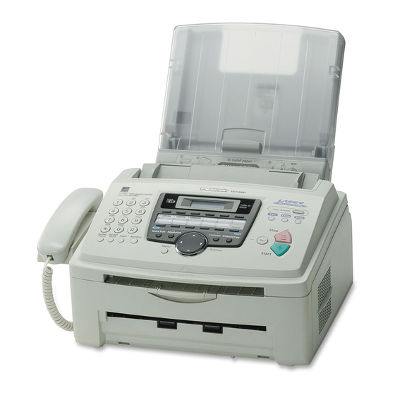
KX-FL612CX / KX-FL612CX-S 3.2. CONNECTIONS (1) Connect the handset cord. (2) Connect the telephone line cord. (3) Connect the power cord. • • • • When the power is turned on for the first time, the unit will print some basic information. -
Page 15: Installation
KX-FL612CX / KX-FL612CX-S 3.3. INSTALLATION 3.3.1. INSTALLATION SPACE The space required to install the unit is shown below. The dimensions given are necessary for the unit to operate efficiently. Note: • • • • Avoid excessive heat or humidity. • • • • Use the unit within the following ranges of temperature and humidity. -
Page 16: Paper Stacker
KX-FL612CX / KX-FL612CX-S 3.3.2. PAPER STACKER Line up the slots ( ) in the paper stacker with the pegs ( ) on the bottom of the unit, then insert the two tabs of the paper stacker into the slots on the unit ( ). - Page 17 KX-FL612CX / KX-FL612CX-S 3.3.4. PAPER TRAY AND PAPER TRAY COVER Insert the paper tray ( ) into the slot ( ) on the back of the unit. Pull the tension plate forward ( ) and attach the paper tray cover ( ), then push the tension plate back ( ).
- Page 18 KX-FL612CX / KX-FL612CX-S 3.3.5. INSTALLING THE RECORDING PAPER A4, Letter or legal size recording paper can be used for fax messages. The unit can hold up to 250 sheets of 60/75 g/m paper, 230 sheets of 80 g/m or 200 sheets of 90 g/m paper.
- Page 19 KX-FL612CX / KX-FL612CX-S Insert the paper, print-side down ( ). • • • • The paper should not be over the tabs ( ). • • • • If the paper is not inserted correctly, readjust the paper, or the paper may jam.
- Page 20 KX-FL612CX / KX-FL612CX-S 3.3.6. DOCUMENTS THE UNIT CAN SEND 3.3.6.1. USING THE ADF (AUTO DOCUMENT FEEDER) Note: • • • • Remove chips, staples or other similar fasteners. • • • • Do not send the following types of documents. (Use copies for fax transmission.) —...
- Page 21 KX-FL612CX / KX-FL612CX-S 3.3.7. TO SELECT CHARACTERS WITH THE DIAL KEYPAD Pressing the dial keys will select a character as shown below. 3.3.8. TO SELECT CHARACTERS USING THE (+) OR (-) KEY...
-
Page 22: Setting Your Logo
KX-FL612CX / KX-FL612CX-S 3.3.9. SETTING YOUR LOGO The logo can be your company, division or name. - Page 23 We recommend you replace the drum unit every fourth time you replace the toner cartridge. To check the drum life and quality, please print the printer test list. To ensure that the unit operates properly, we recommend the use of Panasonic toner cartridge (Model No. KX-FA83E/KX- FA83A) and drum unit (Model No. KX-FA84E/KX-FA84A).
- Page 24 KX-FL612CX / KX-FL612CX-S Lift open the front cover ( ), holding OPEN ( ). Tap on the used toner cartridge several times to allow the remaining toner to fall into the drum unit. Remove the drum and toner unit ( ) by holding the two tabs.
- Page 25 KX-FL612CX / KX-FL612CX-S Remove the used cartridge ( ) from the drum unit ( ). • • • • The toner may stick to the cartridge and the drum unit. Be careful when handling. • • • • Do not drop the toner on the green drum surface ( ).
- Page 26 KX-FL612CX / KX-FL612CX-S • • • • If the lower glass ( ) is dirty, clean it with a soft dry cloth. Install the drum and toner unit ( ) by holding the tabs. Close the front cover ( ) by pushing down on both sides, until locked.
-
Page 27: Maintenance
KX-FL612CX / KX-FL612CX-S 4 MAINTENANCE 4.1. MAINTENANCE ITEMS AND COMPONENT LOCATIONS 4.1.1. OUTLINE MAINTENANCE AND REPAIRS ARE PERFORMED USING THE FOLLOWING STEPS. 1. Periodic maintenance Inspect the equipment periodically and if necessary, clean any contaminated parts. 2. Check for breakdowns Look for problems and consider how they arose. -
Page 28: Maintenance List
KX-FL612CX / KX-FL612CX-S 4.1.2.1. Maintenance List OPERATION CHECK REMARKS Document Path Remove any foreign matter such as paper. — Rollers If the roller is dirty, clean it with a damp cloth then dry Refer to MAINTENANCE CHECK thoroughly. ITEMS/COMPONENT LOCATIONS( P.27).() -
Page 29: Printing
KX-FL612CX / KX-FL612CX-S 4.2. PRINTING • • • • The motor pinion rotates in the direction shown in the figure. • • • • The gears of fixing and developing parts are driven by the GEAR IDLER 67. • • • • The GEAR PAPER FEED ROLLER drives the roller. -
Page 30: Printing (Paper Pick Up)
KX-FL612CX / KX-FL612CX-S 4.3. PRINTING (PAPER PICK UP) During printing • • • • When the SOLENOID is turned ON, the LEVER PICK UP CLUTCH is hooked on the RING of GEAR CLUTCH. It causes the GEAR PICKUP PAPER to rotate. -
Page 31: Scanning (Adf)
KX-FL612CX / KX-FL612CX-S 4.4. SCANNING (ADF) • • • • DOCUMENT TRANSMISSION (ADF) When the tip of the document is set to a point of contact between the separation roller and the separation pad through the document feed roller, then the document is fed there separately. The document feed roller carries the document... -
Page 32: Maintenance
KX-FL612CX / KX-FL612CX-S 4.5. MAINTENANCE If a black line, a white line or a dirty pattern appears on your recording paper, on your original, or on the fax document received by the other party, clean the white plate, scanner glass and lower glass. - Page 33 KX-FL612CX / KX-FL612CX-S Clean the document feeder roller ( ) with a cloth moistened with isopropyl rubbing alcohol, and let all parts dry thoroughly. Clean the upper glass ( ) with a soft and dry cloth. Push back the inner cover.
- Page 34 KX-FL612CX / KX-FL612CX-S Close the front cover ( ) by pushing down on both sides, until locked. Reconnect the power cord and the telephone line cord. Note: • • • • Do not touch the transfer roller ( ).
-
Page 35: Document Jams
KX-FL612CX / KX-FL612CX-S 4.6. DOCUMENT JAMS If the unit does not release the document during feeding, remove the jammed document as follows. Lift open the front cover ( ), holding OPEN ( ). Hold the center part of the front cover ( ), and pull open the inner cover ( ). -
Page 36: Recording Paper Jams
KX-FL612CX / KX-FL612CX-S Note: • • • • Do not pull out the jammed document forcibly before opening the front cover. 4.7. RECORDING PAPER JAMS 4.7.1. When the recording paper has jammed in the unit If the unit does not eject any recording paper during reception or copying, the recording paper has jammed and the display will show the following massage. - Page 37 KX-FL612CX / KX-FL612CX-S When the recording paper has jammed near the recording paper exit: 2-1. Pull the tension plate forward ( ), then remove the paper tray cover ( ). 2-2. Remove the recording paper ( ), then remove the drum and toner unit ( ) to allow the jammed paper ( ) to pull free from the rear cabinet.
- Page 38 KX-FL612CX / KX-FL612CX-S 2-5. Push back the levers ( ) to the original position. Close the front cover ( ) by pushing down on both sides, until locked. Re-insert the recording paper ( ). • • • • Before re-inserting, make sure to fan and straighten the recording paper.
- Page 39 KX-FL612CX / KX-FL612CX-S 4.7.2. When the recording paper is not fed into the unit properly The display will show the following. Pull the tension plate forward ( ), then remove the paper tray cover ( ). Remove the recording paper ( ).
-
Page 40: Disassembly Instructions
KX-FL612CX / KX-FL612CX-S 5 DISASSEMBLY INSTRUCTIONS... -
Page 41: Upper Main Cabinet Section
KX-FL612CX / KX-FL612CX-S 5.1. UPPER MAIN CABINET SECTION CROSS REFERENCE: A1: HOW TO REMOVE THE OPERATION PANEL ASS’Y (P.43) A2: HOW TO REMOVE THE PICK UP UNIT (P.44) A3: HOW TO REMOVE THE PICK UP ROLLER (P.45) A4: HOW TO REMOVE THE OPERATION BOARD (P.46) A5: HOW TO REMOVE THE LOWER FLAME (P.47) -
Page 42: Lower Main Cabinet Section
KX-FL612CX / KX-FL612CX-S 5.2. LOWER MAIN CABINET SECTION CROSS REFERENCE: B1: HOW TO REMOVE THE BOTTOM PLATE (P.50) B2: HOW TO REMOVE THE ANALOG BOARD (P.50) B3: HOW TO REMOVE THE HIGH VOLTAGE POWER BOARD (P.51) B4: HOW TO REMOVE THE LASER UNIT (P.51) B5: HOW TO REMOVE THE FAN UNIT (P.52) -
Page 43: How To Remove The Operation Panel Ass'y
KX-FL612CX / KX-FL612CX-S 5.3. HOW TO REMOVE THE OPERATION PANEL ASS’Y... -
Page 44: How To Remove The Pick Up Unit
KX-FL612CX / KX-FL612CX-S 5.4. HOW TO REMOVE THE PICK UP UNIT... -
Page 45: How To Remove The Pick Up Roller
KX-FL612CX / KX-FL612CX-S 5.5. HOW TO REMOVE THE PICK UP ROLLER... -
Page 46: How To Remove The Operation Board
KX-FL612CX / KX-FL612CX-S 5.6. HOW TO REMOVE THE OPERATION BOARD... -
Page 47: How To Remove The Lower Flame
KX-FL612CX / KX-FL612CX-S 5.7. HOW TO REMOVE THE LOWER FLAME 5.8. HOW TO REMOVE THE SEPARATION RUBBER... -
Page 48: How To Remove The Transfer Roller
KX-FL612CX / KX-FL612CX-S 5.9. HOW TO REMOVE THE TRANSFER ROLLER... -
Page 49: How To Remove The Separation Roller
KX-FL612CX / KX-FL612CX-S 5.10. HOW TO REMOVE THE SEPARATION ROLLER... -
Page 50: How To Remove The Bottom Plate
KX-FL612CX / KX-FL612CX-S 5.11. HOW TO REMOVE THE BOTTOM PLATE 5.12. HOW TO REMOVE THE ANALOG BOARD... -
Page 51: How To Remove The High Voltage Power Board
KX-FL612CX / KX-FL612CX-S 5.13. HOW TO REMOVE THE HIGH VOLTAGE POWER BOARD 5.14. HOW TO REMOVE THE LASER UNIT... -
Page 52: How To Remove The Fan Unit
KX-FL612CX / KX-FL612CX-S 5.15. HOW TO REMOVE THE FAN UNIT 5.16. HOW TO REMOVE THE LOW VOLTAGE POWER BOARD... -
Page 53: How To Remove The Solenoid
KX-FL612CX / KX-FL612CX-S 5.17. HOW TO REMOVE THE SOLENOID 5.18. HOW TO REMOVE THE HANDSET HOLDER... -
Page 54: How To Remove The Main Motor
KX-FL612CX / KX-FL612CX-S 5.19. HOW TO REMOVE THE MAIN MOTOR... -
Page 55: How To Remove The Fuser Unit
KX-FL612CX / KX-FL612CX-S 5.20. HOW TO REMOVE THE FUSER UNIT... -
Page 56: How To Remove The Cis
KX-FL612CX / KX-FL612CX-S 5.21. HOW TO REMOVE THE CIS... -
Page 57: Note For Assembling
KX-FL612CX / KX-FL612CX-S 5.22. NOTE FOR ASSEMBLING 5.22.1. FCC (DIGITAL BOARD) 5.22.2. DOCUMENT STACKER 5.22.3. THERMOSTAT... -
Page 58: Installation Position Of The Lead
KX-FL612CX / KX-FL612CX-S 5.23. INSTALLATION POSITION OF THE LEAD... -
Page 59: Troubleshooting Guide
KX-FL612CX / KX-FL612CX-S 6 TROUBLESHOOTING GUIDE 6.1. USER RECOVERABLE ERRORS If the unit detects a problem, one or more of the following messages will appear on the display. The explanations given in the [ ] are for servicemen only. DISPLAY MESSAGE CAUSE AND REMEDY •... - Page 60 KX-FL612CX / KX-FL612CX-S DISPLAY MESSAGE CAUSE AND REMEDY • • • • The document is jammed. Remove the jammed document. • • • • Attempted to transmit a document longer than 600 mm (23 5/8”). Press the STOP to remove the document.
-
Page 61: Programming And Lists
KX-FL612CX / KX-FL612CX-S 6.2. PROGRAMMING AND LISTS The programming functions are used to program the various features and functions of the machine, and to test the machine. This facilitates communication between the user and the service man while programming the unit. - Page 62 KX-FL612CX / KX-FL612CX-S 6.2.3. SERVICE FUNCTION TABLE Code Function Set Value Effective Default Remarks Range Pause time set X 100 msec 001~600 ---------- Flash time X 10 ms 01~99 ---------- Bell signal detect time X 100msec ---------- CED frequency select...
- Page 63 KX-FL612CX / KX-FL612CX-S Code Function Set Value Effective Default Remarks Range Paper Jam Cause Distinction Code 0:No Paper Jam 1:The paper was pulled into the unit. 2:The paper was longer than the maximum length of the register sensor. 3:The paper exit was not detected after the registration.
-
Page 64: Test Functions
KX-FL612CX / KX-FL612CX-S 6.3. TEST FUNCTIONS The codes listed below can be used to perform simple checks of some of the unit’s functions. When complaints are received from customers, they provide an effective tool for identifying the locations and causes of malfunctions. - Page 65 KX-FL612CX / KX-FL612CX-S Test Mode Type of Mode Code Function Operation after code input SENSOR CHECK Service Mode “8” “1” “5” First of all, press the copy button, and confirm the action of ON/OFF. For each sensor’s operation, refer to SENSORS AND SWITCHES SECTION (P.175).
- Page 66 KX-FL612CX / KX-FL612CX-S 6.3.1. DTMF SINGLE TONE TRANSMIT SELECTION Note: After performing this check, do not forget to turn the setting off. otherwise, dialing in DTMF signal will not work. 6.3.2. BUTTON CODE TABLE...
-
Page 67: Print Test Pattern
KX-FL612CX / KX-FL612CX-S 6.3.3. PRINT TEST PATTERN 1. NO. 01 3. NO.12 2. NO.08 • • • • These print test patterns are just image printing, and different from actual ones. When it is required to judge the print quality, compare with... -
Page 68: Remote Programming
KX-FL612CX / KX-FL612CX-S 6.4. REMOTE PROGRAMMING If, after the call is connected, the customer describes the situation and it is determined that the problem can be corrected by making parameter changes, this function makes it possible to change parameters such as the user code and service code from another fax (using DTMF tones). - Page 69 KX-FL612CX / KX-FL612CX-S 6.4.2. PROGRAM MODE TABLE Code Function Set Value Default Remote Setting Set date and time mm/dd/yy hh:mm Jan/01/2005 Your logo --------- None Your fax telephone number --------- None Transmission report mode 2:ON / 3:OFF / 1:ERROR ERROR...
- Page 70 KX-FL612CX / KX-FL612CX-S Code Function Set Value Default Remote Setting Receive speed select 1:14400/ 2:12000/ 3:9600/ 4:7200/ 14400bps 5:4800/ 6:2400 Pause tone detect 1:ON / 2:OFF Redial tone detect 1:ON / 2:OFF CNG detect time for friendly reception 1:10s / 2:20s / 3:30s...
- Page 71 KX-FL612CX / KX-FL612CX-S 6.4.3. USER MODE (The list below is an example of the SYSTEM SETUP LIST the unit prints out.) Note: The above values are the default values.
- Page 72 KX-FL612CX / KX-FL612CX-S 6.4.4. SERVICE MODE SETTINGS (Example of a printed out list) Note: The above values are the default values.
- Page 73 KX-FL612CX / KX-FL612CX-S 6.4.5. HISTORY (Example of a printed out list) Note: See the following descriptions of this report. Item No. (1) ~ (54) are corresponding to the listed items in DESCRIPTIONS OF THE HISTORY REPORT(P.74).
- Page 74 KX-FL612CX / KX-FL612CX-S 6.4.5.1. DESCRIPTIONS OF THE HISTORY REPORT (1) ROM VERSION FLASH ROM version (2) SUM FLASH ROM internal data calculation. (3) YOUR LOGO The user logo recorded in the unit. If it is not recorded, NONE will be displayed.
- Page 75 KX-FL612CX / KX-FL612CX-S (28) Not used (29) Not used (30) Not used (31) NUMBER OF PRINTING HELP The number of help lists printed until now. (32) NUMBER OF DIVIDED PRINTING IN FAX RECEPTION The number of faxes received that were divided into more than one sheet since the unit was purchased.
-
Page 76: Troubleshooting Details
KX-FL612CX / KX-FL612CX-S 6.5. TROUBLESHOOTING DETAILS 6.5.1. OUT LINE Troubleshooting is for recovering quality and reliability by determining the broken component and replacing, adjusting or cleaning it as required. First, determine the problem then decide the troubleshooting method. If you have difficulty finding the broken part, determine which board is broken. - Page 77 KX-FL612CX / KX-FL612CX-S 6.5.3. INITIALIZATION There are two types of initialization, one is the short initialization (about 3 seconds) and the other is the long initialization (about 10 seconds). The short initialization makes the unit enter the standby mode. The long initialization makes the unit enter the...
- Page 78 KX-FL612CX / KX-FL612CX-S 6.5.4. SIMPLE CHECK LIST Note: Check according to the service code referring to TEST FUNCTIONS (P.64)
- Page 79 KX-FL612CX / KX-FL612CX-S 6.5.5. SIMPLIFIED TROUBLESHOOTING GUIDE 6.5.5.1. PRINTING Symptom Cause Countermeasure 1 GHOST IMAGE (P.88) Failed drum unit Replace drum unit Failed transfer unit Check the transfer roller and spring Failed the high-voltage terminal Check the high-voltage terminal Failed the high voltage power supply board Go to HIGH VOLTAGE SECTION (P.140)
- Page 80 KX-FL612CX / KX-FL612CX-S 6.5.5.2. RECORDING PAPER FEED Symptom Cause Countermeasure 1 MULTIPLE FEED (P.96) Dirty or failed the pickup roller Clean or replace the pickup roller Dirty or failed the pickup rubber Clean or replace the separation rubber 2 THE RECORDING PAPER...
- Page 81 KX-FL612CX / KX-FL612CX-S 6.5.5.3. COPY AND FAX Symptom Cause Countermeasure 1 NO DOCUMENT FEED Failed the document sensor lever Replace the document sensor lever (NO DOCUMENT Failed the document sensor Go to DOCUMENT SENSOR (P.161) FEED,DOCUMENT JAM Dirty or failed the separation roller...
- Page 82 KX-FL612CX / KX-FL612CX-S 6.5.5.4. Others Symptom Cause Countermeasure 1 Cannot print legal size Not selected the legal mode Select the legal mode in the user programming mode 2 ´CHECK DRUM´ on the The drum unit can not be detected. Go to DRUM SENSOR (P.177) •...
- Page 83 KX-FL612CX / KX-FL612CX-S 6.5.6. CALL SERVICE TROUBLESHOOTING GUIDE Call Service related error is most frequent. Call Service 1 ----- Polygon doesn’t rotate..Refer to LSU (Laser Scanning Unit) SECTION (P.173). • • • • First, listen to the sound. If rotation sound isn´t heard, check 24V line, POLON signal and POLCLK signal. If even a little of sound is heard, check XREADY signal.
-
Page 84: Call Service
KX-FL612CX / KX-FL612CX-S 6.5.6.1. CALL SERVICE 1 "CALL SERVICE 1" means that the polygon motor inside the LSU does not rotate. The rotation of the polygon motor is detected by IC606-32pin (XREADY). - Page 85 KX-FL612CX / KX-FL612CX-S 6.5.6.2. CALL SERVICE 2 "CALL SERVICE 2" means that the synchronous signal out of the LSU cannot be detected. The synchronous signal out of the LSU is detected by IC 606-33pin. (XHSYNC) Note: As for the "Pulse" waveform of the above flow chart, see the timing chart.
- Page 86 KX-FL612CX / KX-FL612CX-S 6.5.6.3. CALL SERVICE 3 "CALL SERVICE 3" means that the temperature of the fuser does not rise up to or exceed a constant temperature. The temperature is monitored with the thermistor inside the fuser and detected with the voltage input into IC 606-4pin.
- Page 87 KX-FL612CX / KX-FL612CX-S 6.5.6.4. CALL SERVICE 4 "CALL SERVICE 4" means that the FAN does not run or the running of the FAN cannot be detected normally. The running of the FAN is detected by IC 605-91pin. "CALL SERVICE 4" is displayed when it detects NG five times continuously.
-
Page 88: Ghost Image
KX-FL612CX / KX-FL612CX-S 6.5.7. PRINT 6.5.7.1. GHOST IMAGE CROSS REFERENCE: HIGH VOLTAGE SECTION(P.140) POWER SUPPLY BOARD SECTION(P.144) - Page 89 KX-FL612CX / KX-FL612CX-S 6.5.7.2. DARK OR WHITE VERTICAL LINE Note: When wiping the lower glass, reflecting mirror and LSU lens, use a dry and soft cloth. CROSS REFERENCE: LSU SECTION (P.137)
- Page 90 KX-FL612CX / KX-FL612CX-S 6.5.7.3. DARK OR WHITE HORIZONTAL LINE CROSS REFERENCE: HIGH VOLTAGE SECTION (P.140)
- Page 91 KX-FL612CX / KX-FL612CX-S 6.5.7.4. DIRTY OR HALF DARKNESS BACKGROUND CROSS REFERENCE: HIGH VOLTAGE SECTION (P.140)
-
Page 92: Black Print
KX-FL612CX / KX-FL612CX-S 6.5.7.5. BLACK PRINT CROSS REFERENCE: HIGH VOLTAGE SECTION (P.140) LSU SECTION (P.137) -
Page 93: Light Print
KX-FL612CX / KX-FL612CX-S 6.5.7.6. LIGHT PRINT CROSS REFERENCE: HIGH VOLTAGE SECTION (P.140) - Page 94 KX-FL612CX / KX-FL612CX-S 6.5.7.7. BLACK DENSITY IS LIGHT OR UNEVEN CROSS REFERENCE: HIGH VOLTAGE SECTION (P.140)
- Page 95 KX-FL612CX / KX-FL612CX-S 6.5.7.8. BLANK PRINT 6.5.7.9. BLACK OR WHITE POINT...
- Page 96 KX-FL612CX / KX-FL612CX-S 6.5.8. RECORDING PAPER FEED 6.5.8.1. MULTIPLE FEED 6.5.8.2. THE RECORDING PAPER IS WAVED OR WRINKLED...
- Page 97 KX-FL612CX / KX-FL612CX-S 6.5.8.3. SKEW...
- Page 98 KX-FL612CX / KX-FL612CX-S 6.5.8.4. THE RECORDING PAPER DOES NOT FEED CROSS REFERENCE: SENSOR SECTION (P.132) MOTOR SECTION (P.135)
- Page 99 KX-FL612CX / KX-FL612CX-S 6.5.8.5. THE RECORDING PAPER JAM CROSS REFERENCE: mode *630 distinguishes the cause. PAPER EXIT SENSOR..“PAPER JAMMED” (P.179) 0:No Paper Jam FAN MOTOR SECTION (P.170) 1:Failed pick up REGIST SENSOR (P.178) 2:The paper top sensor is not turned OFF although the fixed time had passed since the sensor was turned ON.
- Page 100 KX-FL612CX / KX-FL612CX-S 3:The paper eject sensor is not turned ON although the fixed time had passed since the paper top sensor was turned ON. 4:The paper eject sensor is not turned OFF although the fixed time had passed since it was turned ON.
- Page 101 KX-FL612CX / KX-FL612CX-S 6.5.8.6. BACK SIDE OF THE RECORDING PAPER IS DIRTY CROSS REFERENCE: HIGH VOLTAGE SECTION (P.140)
- Page 102 KX-FL612CX / KX-FL612CX-S 6.5.9. ADF (Auto document feed) SECTION 6.5.9.1. NO DOCUMENT FEED,DOCUMENT JAM and MULTIPLE DOCUMENT FEED. CROSS REFERENCE: SENSOR SECTION (P.132)
- Page 103 KX-FL612CX / KX-FL612CX-S CROSS REFERENCE: MOTOR SECTION (P.135)
- Page 104 KX-FL612CX / KX-FL612CX-S 6.5.9.2. SKEW (ADF)
- Page 105 KX-FL612CX / KX-FL612CX-S 6.5.9.3. THE SENT FAX DATA IS SKEWED CROSS REFERENCE: SKEW (ADF) (P.104) 6.5.9.4. THE RECEIVED FAX DATA IS SKEWED CROSS REFERENCE: SKEW (P.97)
- Page 106 KX-FL612CX / KX-FL612CX-S 6.5.9.5. THE RECEIVED OR COPIED DATA IS EXPANDED...
- Page 107 KX-FL612CX / KX-FL612CX-S 6.5.9.6. BLACK OR WHITE VERTICAL LINE IS COPIED...
- Page 108 KX-FL612CX / KX-FL612CX-S 6.5.9.7. AN ABNORMAL IMAGE IS COPIED CROSS REFERENCE: CIS (Contact Image Sensor) SECTION (P.138)
- Page 109 KX-FL612CX / KX-FL612CX-S 6.5.10. COMMUNICATION SECTION Find the problem in the table shown below, and refer to the corresponding troubleshooting procedure in DEFECTIVE FACSIMILE SECTION (P.110). Symptom Content Possible cause The paper dose not feed properly when faxing. Troubleshooting Problem with the feeding (Copying is also not possible.)
- Page 110 KX-FL612CX / KX-FL612CX-S 6.5.10.1. DEFECTIVE FACSIMILE SECTION 6.5.10.1.1. TRANSMIT PROBLEM CROSS REFERENCE: CLEANING THE INSIDE OF THE UNIT (P.32) ADF (Auto document feed) SECTION (P.102) OPERATION PANEL SECTION (P.131)
- Page 111 KX-FL612CX / KX-FL612CX-S 6.5.10.1.2. SOMETIME THERE IS A TRANSMIT PROBLEM Note: “596: Transmit level set” represents a service code. Refer to the SERVICE FUNCTION TABLE (P.62). “717: Transmit speed select” represents a service code. Refer to the SERVICE FUNCTION TABLE (P.62).
- Page 112 KX-FL612CX / KX-FL612CX-S 6.5.10.1.3. RECEIVE PROBLEM Confirm the following before starting troubleshooting. • • • • Is the recording paper installed properly? Refer to the next page. Note: “596: Transmit level set” represents a service code. Refer to the SERVICE FUNCTION TABLE (P.62).
- Page 113 KX-FL612CX / KX-FL612CX-S For the receiving problem, we have thought of causes other than in the software. Some causes may be when the fax changes to the memory receiving mode (for example, when out of paper). and the memory becomes full of the unprinted fax data. In this case, [MEMORY FULL] and its main cause (for example, “OUT OF PAPER”) are displayed on the LCD.
- Page 114 KX-FL612CX / KX-FL612CX-S 6.5.11. SPECIAL SERVICE JOURNAL REPORTS Journal 2 and Journal 3 shown below, which are special journals giving the additional detailed information about the latest 35 communications, can be printed by Service Code 881 or 882. Remote printing function for the journal reports (JOURNAL, JOURNAL 2 and JOURNAL 3) is also available for service technicians.
- Page 115 KX-FL612CX / KX-FL612CX-S 6.5.11.1. JOURNAL 2 Refer to JOURNAL 2 in PRINTOUT EXAMPLE(P.116). Journal 2 displays the additional detailed information about the last 35 communications. Descriptions: (1) RCV. MODE Indicates which receive mode the unit was in when the unit received a fax message.
- Page 116 KX-FL612CX / KX-FL612CX-S 6.5.11.2. JOURNAL 3 Refer to JOURNAL 3 in PRINTOUT EXAMPLE(P.116). Description (6) ENCODE (9) ERROR LINE (RX) Compression Code: MH/MR/MMR When an error occurs while receiving a fax, this shows the number of error lines. (7) MSLT (10) MAKER CODE MSLT means Minimum Scan Line Time.
- Page 117 KX-FL612CX / KX-FL612CX-S...
- Page 118 KX-FL612CX / KX-FL612CX-S 6.5.11.4. HOW TO OUTPUT THE JOURNAL REPORT 1. Press the MENU button. 2. Press “#”, then “8” and “3”. 3. Press the START/COPY/SET button. 4. The report prints out. CROSS REFERENCE: FEATURES(P.10) Error code table: (1) CODE...
- Page 119 KX-FL612CX / KX-FL612CX-S Note*: If the problem remains, see the following “Countermeasure” flow chart.
- Page 120 KX-FL612CX / KX-FL612CX-S CROSS REFERENCE: TEST FUNCTIONS (P.64)
- Page 121 KX-FL612CX / KX-FL612CX-S CROSS REFERENCE: TEST FUNCTIONS (P.64)
- Page 122 KX-FL612CX / KX-FL612CX-S CROSS REFERENCE: TEST FUNCTIONS (P.64)
- Page 123 KX-FL612CX / KX-FL612CX-S CROSS REFERENCE: TEST FUNCTIONS (P.64)
- Page 124 KX-FL612CX / KX-FL612CX-S...
- Page 125 KX-FL612CX / KX-FL612CX-S...
- Page 126 KX-FL612CX / KX-FL612CX-S CROSS REFERENCE: TEST FUNCTIONS (P.64)
- Page 127 KX-FL612CX / KX-FL612CX-S 6.5.12. INITIALIZING ERROR After the power is turned on, the ASIC (IC606) initializes and checks each IC. The ROM (IC607), SDRAM (IC604), and MODEM (IC600) are checked. If initialization fails for the ICs, the system will not boot up.
- Page 128 KX-FL612CX / KX-FL612CX-S 6.5.13. ANALOG BOARD SECTION This chapter provides the testing procedures required for the analog parts. A signal route to be tested is determined depending upon purposes. For example, the handset TX route begins at the handset microphone and the signal is output to the telephone line.
- Page 129 KX-FL612CX / KX-FL612CX-S 6.5.13.2. DEFECTIVE ITS (Integrated Telephone System) SECTION 1. No handset and speakerphone transmission / reception Perform a signal test in the ITS or the NCU section and locate a defective point (where the signal disappears) on each route...
- Page 130 KX-FL612CX / KX-FL612CX-S 6.5.13.3. DETECTIVE TAM INTERFACE SECTION 1. The FAX turns on, but does not arrive through TAM. CROSS REFERENCE: TAM INTERFACE SECTION (P.164) 2. A FAX is received, but won´t switch from TAM to FAX. CROSS REFERENCE: ANALOG BOARD SECTION (P.128)
-
Page 131: Operation Panel Section
KX-FL612CX / KX-FL612CX-S 6.5.13.4. OPERATION PANEL SECTION Refer to TEST FUNCTIONS (P.64). 1. NO KEY OPERATION 2. NO LCD INDICATION CROSS REFERENCE: TEST FUNCTIONS (P.64) - Page 132 KX-FL612CX / KX-FL612CX-S 6.5.13.5. SENSOR SECTION Refer to SENSORS AND SWITCHES for the circuit description. Perform an SENSOR CHECK to determine if the sensor is operating correctly. 1. Check the document sensor ..“CHECK DOCUMENT” 2. Check the paper feed sensor..“REMOVE DOCUMENT”...
- Page 133 KX-FL612CX / KX-FL612CX-S 5. Check the DRUM sensor..“CHECK DRUM” 6. Check the regist sensor..“FAILED PICKUP” 7. Check the paper sensor..“OUT OF PAPER” 8. Check the exit switch..“PAPER JAMMED”...
- Page 134 KX-FL612CX / KX-FL612CX-S 9. Check the toner sensor..“TONER LOW”, “CHANGE DRUM” As for the following check, remove the drum from the main body, set it again and close the cover, then perform that check during initializing operation. Refer to SENSORS AND SWITCHES SECTION (P.175).
- Page 135 KX-FL612CX / KX-FL612CX-S 6.5.13.6. MOTOR SECTION 6.5.13.6.1. ENGINE MOTOR...
-
Page 136: Adf Motor
KX-FL612CX / KX-FL612CX-S 6.5.13.6.2. ADF MOTOR... - Page 137 KX-FL612CX / KX-FL612CX-S 6.5.13.7. LSU SECTION CROSS REFERENCE: LSU (Laser Scanning Unit) SECTION (P.173)
- Page 138 KX-FL612CX / KX-FL612CX-S 6.5.14. CIS (Contact Image Sensor) SECTION CROSS REFERENCE: TEST FUNCTIONS (P.64)
- Page 139 KX-FL612CX / KX-FL612CX-S 6.5.15. HIGH VOLTAGE VALUE CHECK POINT Measurement Procedure 1. Open the TOP cover. 2. Remove the developing unit, if it is equipped. 3. Open the TOP cover, and turn ON the TOP cover SW. (Push the TOP cover SW with a sharp-tipped insulator or insert folded paper, etc. to the slit.) 4.
-
Page 140: High Voltage Section
KX-FL612CX / KX-FL612CX-S 6.5.16. HIGH VOLTAGE SECTION... - Page 141 KX-FL612CX / KX-FL612CX-S...
- Page 142 KX-FL612CX / KX-FL612CX-S...
- Page 143 KX-FL612CX / KX-FL612CX-S * This Adjustment should be done with a single High Voltage Board. * As for the High Voltage Probe, HV PROBE 9014 of HIOKI electric co. or the equivalent should be used. * As for the tester, FLUKE 85 III multi meter or the equivalent should be used.
- Page 144 KX-FL612CX / KX-FL612CX-S 6.5.17. POWER SUPPLY BOARD SECTION 6.5.17.1. KEY COMPONENTS FOR TROUBLESHOOTING Check the following parts first: F101, D101-D104, C106, Q101, PC101 and IC101. This comes from our experience with experimental tests. For example: power supply and lightning surge voltage test, withstanding voltage test, intentional short circuit test, etc.
-
Page 145: Troubleshooting Flow Chart
KX-FL612CX / KX-FL612CX-S 6.5.17.2. TROUBLESHOOTING FLOW CHART... - Page 146 KX-FL612CX / KX-FL612CX-S 6.5.17.3. BROKEN PARTS REPAIR DETAILS (D101~D104) Check for a short-circuit in terminal 4. If D101~D104 is short-circuit, F101 will melt (open). In this case, replace all of the parts (D101~D104, F101). (Q101) The worst case of Q101 is a short-circuit between the Drain and Gate because damage expands to the peripheral circuit of Q101.
-
Page 147: Circuit Operations
KX-FL612CX / KX-FL612CX-S 7 CIRCUIT OPERATIONS 7.1. CONNECTION DIAGRAM... -
Page 148: General Block Diagram
KX-FL612CX / KX-FL612CX-S 7.2. GENERAL BLOCK DIAGRAM The following is an outline of each device IC on the digital board. 1. ASIC (IC606) This custom IC is used for general FAX operations. (1) CPU: This model uses a Z80 equivalent CPU operating at 16MHz. - Page 149 KX-FL612CX / KX-FL612CX-S...
-
Page 150: Facsimile Section
KX-FL612CX / KX-FL612CX-S 7.3. FACSIMILE SECTION 7.3.1. DIGITAL SECTION 7.3.1.1. DIGITAL BLOCK DIAGRAM CN610 CN607 CN613 TO TXMOTOR TO PC TO SMPS +24V MOTOR DRIVER IC610 RESET/REGULATOR RESET IC607 IC608 XROMCS +3.3V PC I/F RESET +3.3V SDRAM +2.5V IC604 SDCLK etc... - Page 151 KX-FL612CX / KX-FL612CX-S 7.3.1.2. ASIC (IC606) This custom IC is used for general FAX operations. (1) CPU: This model uses a Z80 equivalent CPU operating at 16MHz. Many of the peripheral functions are handled by custom designed LSIs. As a result,the CPU only needs to process the results.
- Page 152 KX-FL612CX / KX-FL612CX-S SIGNAL POWER SUPPLIED EXPLANATION VOLTAGE TM1/IOP11 3.3V TX MOTOR CONTROL TM2/IOP12 3.3V TX MOTOR CONTROL TM3/IOP13 3.3V TX MOTOR CONTROL TXE/IOP14 3.3V TX MOTOR POWER CONTROL VDD2.5V 2.5V POWER SOURCE TRS/OP06 3.3V TRANSFER BIAS CONTROL HTRCTL 3.3V...
- Page 153 KX-FL612CX / KX-FL612CX-S SIGNAL POWER SUPPLIED EXPLANATION VOLTAGE ADR4 3.3V ADDRESS BUS 4 ADR5 3.3V ADDRESS BUS 5 ADR6 3.3V ADDRESS BUS 6 ADR7 3.3V ADDRESS BUS 7 ADR8 3.3V ADDRESS BUS 8 ADR9 3.3V ADDRESS BUS 9 ADR10 3.3V...
- Page 154 KX-FL612CX / KX-FL612CX-S SIGNAL POWER SUPPLY EXPLANATION VOLTAGE SENIN2/IOP02 INPUT PORT(BELL) SENIN3/IOP03 INPUT PORT(TNREMP) IOP63/XCBUSY1 NOT USED IOP64/XCBUSY2 NOT USED IOP30(XHSYNC) INPUT PORT(XHSYNC) IOP31 NOT USED IOP32 OUTPUT PORT(CISON) POWER SOURCE IOP33 OUTPUT PORT(CISLEDON) IOP34 INPUT PORT(DRUM) IOP35 OUTPUT PORT(PICKUP)
- Page 155 KX-FL612CX / KX-FL612CX-S SIGNAL POWER SUPPLY EXPLANATION VOLTAGE KSCLK 3.3V OPERATION PANEL CONTROL KTXD 3.3V OPERATION PANEL CONTROL KRXD/IP23/SENIN3 3.3V INPUT FROM READ POSITION SENSOR 3.3V 3.3V 3.3V POWER SOURCE VIN0/IP20(APC) 3.3V INPUT TO INVERTER VIN1/IP21 3.3V INPUT TO INVERTER VIN2/IP22 3.3V...
- Page 156 KX-FL612CX / KX-FL612CX-S 7.3.2. RTC BACKUP CIRCUIT 1. Function This unit has a lithium battery (BAT600) which works for the Real Time Clock IC (RTC: inside IC606). The RTC continues to work, backed up by a lithium battery even when the power switch is OFF.
- Page 157 KX-FL612CX / KX-FL612CX-S 7.3.3. MODEM CIRCUIT OPERATION The modem (IC600) has all the hardware satisfying the CCITT standards mentioned previously. When the ASIC IC606 (114) is brought to a low level, the modem (IC600) is chip-selected and the resistors inside IC are selected by the select signals from ASIC (IC606) ADR0-ADR4(pin 84~88).
- Page 158 KX-FL612CX / KX-FL612CX-S 7.3.4. ANALOG SECTION Composed of ITS circuit and NCU circuit. 7.3.4.1. ANALOG GATE ARRAY (IC207) The cross-point switch installed in this IC makes it possible to change the circuit configuration for any analog signals such as the fax signals sent from the digital board. In addition, this analog gate array integrates a handset circuit, input/output ports, etc.
- Page 159 KX-FL612CX / KX-FL612CX-S 7.3.4.2. DESCRIPTION OF BLOCK DIAGRAM IN ANALOG SECTION 1. Function The analog section works as an interface between the telephone line. The analog ASIC (IC207) on the analog board exchanges FAX TX and RX signals between the MODEM (IC600) and the analog section.
-
Page 160: Block Diagram
KX-FL612CX / KX-FL612CX-S 7.3.4.3. BLOCK DIAGRAM... -
Page 161: Ncu Section
KX-FL612CX / KX-FL612CX-S 7.4. NCU SECTION 7.4.1. GENERAL This section is the interface between the telephone line and external telephone. It is composed of an EXT. TEL line relay (RLY200), bell detection circuit, TAM interface circuit, line amplifier and side tone circuits and a multiplexer. - Page 162 KX-FL612CX / KX-FL612CX-S 7.4.5. LINE AMPLIFIER AND SIDE TONE CIRCUIT 1. Circuit Operation The reception signal output from the line transformer T201 is input to pin (2) of IC204 via C232, R236 and then the signal is amplified at pin (1) of IC204 and sent to the reception system.
-
Page 163: Its (Integrated Telephone System) And Monitor Section
KX-FL612CX / KX-FL612CX-S 7.4.7. REMOTE FAX ACTIVATION CIRCUIT 1. Function Another telephone connected to same line activates the unit to the FAX mode by using a DTMF signal. 2. Signal Path Refer to CHECK SHEET (P.128). 7.4.8. TAM INTERFACE CIRCUIT This circuit is to switch between FAX receiving and the external TAM’s message recording automatically. - Page 164 KX-FL612CX / KX-FL612CX-S 7.5.1.2. HANDSET CIRCUIT 1. Function This circuit controls the conversation over the handset, i.e. the transmitted and received voices to and from the handset. 2. Signal Path (Transmission signal) Refer to CHECK SHEET. 3. Signal path (Reception signal) Refer to CHECK SHEET.
-
Page 165: Cis Control Section
KX-FL612CX / KX-FL612CX-S 7.6. CIS CONTROL SECTION The scanning block of this device consists of a control circuit and a contact image sensor made up of a celfoc lens array, an LED, a light guide, and photoelectric conversion elements. When an original document is inserted and the start button pressed, pin 15 of IC605 goes to a high level and the transistor Q618 turns on.This applies voltage to the LED to light it. -
Page 166: Stepping Motor Drive Section
KX-FL612CX / KX-FL612CX-S 7.7. STEPPING MOTOR DRIVE SECTION 7.7.1. ENGINE MOTOR DRIVE CIRCUIT 1. Functions This motor functions for main operations FAX reception and copy printing. This feed recording paper synchronized for printing. 2. Motor operation Excitation pulses is output from G/A (IC605) pins 83, 84, 85 and 86. Then stepping pulses are output from driver IC (IC609) pin No 2, 7, 8 and 13, and drives the motor coil. - Page 167 KX-FL612CX / KX-FL612CX-S 7.7.1.2. ENGINE MOTOR DRIVE CIRCUIT...
-
Page 168: Timing Chart
KX-FL612CX / KX-FL612CX-S 7.7.2. SCAN MOTOR DRIVE CIRCUIT 1. Functions This motor functions for main operations including FAX transmission. This feed document paper synchronized for reading. 2. Motor operation During motor driving, pin 25 of ASIC IC606 becomes a high level, and Q613, Q620 turns ON. - Page 169 KX-FL612CX / KX-FL612CX-S 7.7.2.2. SCAN MOTOR (ADF MOTOR) DRIVE CIRCUIT DRIVE MODE FUNCTION MODE PHASE PATTERN SPEED SCAN STANDARD 2 phase 579pps SCAN FAX/COPY FINE/PHOTO 2 phase 579pps SCAN FAX/COPY SUPER FINE 1-2 phase 579pps SCAN FAX/COPY PHOTO WITH TEXT...
-
Page 170: Fan Motor Section
KX-FL612CX / KX-FL612CX-S 7.8. FAN MOTOR SECTION This FAN is used to radiate heat in the unit. The signal level at pin 92/94 of IC605 becomes high, the FAN is activated. In this case, the pulse signal as shown below input... -
Page 171: Fan Control
KX-FL612CX / KX-FL612CX-S 7.8.1. FAN CONTROL This unit is equipped with fan to prevent the developing device from rising in temperature while printing. The air is inhaled from the right side of the unit. The fan rotates at high speed (Approx. 3000 rpm) while printing (controlling the developing device). After printing is finished, it rotates at low speed (Approx. -
Page 172: Solenoid Drive Section
KX-FL612CX / KX-FL612CX-S 7.9. SOLENOID DRIVE SECTION The solenoid drive circuit controls the pick-up clutch. The solenoid is designed to be driven by +24V, driven by IC605-17 pin. Diode D600 protects Q607 from backward voltage when the solenoid is driven. -
Page 173: Lsu (Laser Scanning Unit) Section
KX-FL612CX / KX-FL612CX-S 7.10. LSU (Laser Scanning Unit) SECTION... - Page 174 KX-FL612CX / KX-FL612CX-S...
-
Page 175: Sensors And Switches Section
KX-FL612CX / KX-FL612CX-S 7.11. SENSORS AND SWITCHES SECTION All of the sensor and switches are shown below. Sensor Circuit Location Sensor Sensor or Switch Name Message Error Operation Panel PS101 Document set [CHECK DOCUMENT] Operation Panel SW146 Paper Feed [REMOVE DOCUMENT]... -
Page 176: Document Sensor
KX-FL612CX / KX-FL612CX-S 7.11.2. DOCUMENT SENSOR The Sensor detects whether or not a document is in place. When a document is detected, the shelter plate shuts off the sensor light, the photo-transistor turns OFF, and the input signal of IC101-19pin becomes a high level. When there is no document, the shelter plate let the sensor light pass through, the photo- transistor turns ON, and the input signal of IC101-19pin becomes a low level. - Page 177 KX-FL612CX / KX-FL612CX-S 7.11.4. TOP COVER OPEN SWITCH The Switches detect whether the printer cover is open or closed. When the printer cover is closed, the switches turn ON, and the input signal of IC605-37pin becomes a high level. When the printer cover is open, the switches turns OFF, and the input signal of IC605-37pin becomes a low level.
- Page 178 KX-FL612CX / KX-FL612CX-S 7.11.6. REGIST SENSOR The Sensor detects whether or not the recording paper is present so that printing can start. When the recording paper is detected, the shelter plate let the sensor light passing through, the photo-transistor turns ON, and the input signal of IC605-5pin becomes a low level.
- Page 179 KX-FL612CX / KX-FL612CX-S 7.11.7. PAPER SENSOR..“OUT OF PAPER” The Sensor detects the recording paper are in place. When the recording paper is detected, the shelter plate let the sensor light passing through, the photo-transistor turns ON, and the input signal of IC605-35 pin becomes a low level.
- Page 180 KX-FL612CX / KX-FL612CX-S 7.11.9. Detecting New Drum Units Purpose To investigate the actual number of printed papers with the drum units (Investigating how the returned sets´ drum units were used) Method Whether the drum unit is new or old should be judged by detecting the turn delay of Mixing Paddle (Toner detection sensor).
- Page 181 KX-FL612CX / KX-FL612CX-S...
- Page 182 KX-FL612CX / KX-FL612CX-S 7.11.10. TONER SENSOR..“TONER EMPTY”, “TONER LOW”, “CHANGE DRUM” The Sensor detects whether or not the Drum unit and the toner are present. When there is not Drum unit, Hall IC (IC60) turns off, and the input signal of IC605-7 pin (Digital P.C.B) becomes a High level over 9s.
- Page 183 KX-FL612CX / KX-FL612CX-S 7.11.10.1. TONER DETECTION FLOW CAUTION: 1. Toner low can be judged by continuous 5-times TONER LOW signal at only printing. (It is not executed at.) 2. Toner full can be judged by continuous 3-times TONER FULL signal at initialization.
-
Page 184: Operation Board Section
KX-FL612CX / KX-FL612CX-S 7.12. OPERATION BOARD SECTION The unit consists of a LCD (Liquid crystal display), KEYs and LEDs (light-emitting diodes). They are controlled by the Gate Array (IC101) and Gate Array (IC605: on the DIGITAL BOARD). The key matrix table is shown below. -
Page 185: Lcd Section
KX-FL612CX / KX-FL612CX-S 7.13. LCD SECTION The Gate Array (IC101) works only for writing the ASCII code from the data bus (D4~D7). V0 is supplied for the crystal drive. R130 and R134 are density control resistors. Consequently, in this unit, the timing (positive clock) is generated by the LCD interface circuitry in the gate array (IC101). -
Page 186: Hvps (High Voltage Power Supply) Section
KX-FL612CX / KX-FL612CX-S 7.14. HVPS (High Voltage Power Supply) SECTION 7.14.1. HVPS SPECIFICATION Output voltage Item Specification Notes Electrostatic Rate output voltage -1000±30V Charge Impedance range 50M~1000MΩ CHG BIAS Output format Constant voltage Developing Rate output voltage -200±15V DEV(-) BIAS Impedance range 10M~2000MΩ... -
Page 187: Developing Unit
KX-FL612CX / KX-FL612CX-S 7.14.2. CHG-BIAS (Charge BIAS)/DEV(-) BIAS (Developing(-) BIAS)/DEV(+) BIAS (Developing(+) BIAS) UNIT When the CHG REM terminal becomes “L”, the transistor Q201 turns ON by IC101, Charge BIAS(-1000V) is output from CHG OUTPUT, Developing(-) BIAS(-200V) is output from DEV(-) BIAS. After that, when DEV CHG terminal becomes “L”, Q202 turns ON, and Developing(+) BIAS(+150V) is output from DEV(+) BIAS. -
Page 188: Heat Lamp Control Circuit
KX-FL612CX / KX-FL612CX-S 7.15. HEAT LAMP CONTROL CIRCUIT The temperature of the fixing part of the Fixing Unit is converted to a voltage by THERMISTOR and input to IC606-4pin. The heater turns ON/OFF the photo-coupler PC102 at the heater control port (IC606-29pin), and is turned ON/OFF at the triac SCR101. - Page 189 KX-FL612CX / KX-FL612CX-S 2. Safety Protection a. 2 thermostats are provided with the unit, and the heater circuit is shut down when their surface temperatures became over...
- Page 190 KX-FL612CX / KX-FL612CX-S 135°C. b. The heater control circuit of IC606 has the built-in function that the software turns off the heater control automatically if the heater is not turned ON every a fixed time. c. When the temperature became over 240°C, the heater control circuit of IC606 is turned off forcedly and system reset (IC606...
- Page 191 KX-FL612CX / KX-FL612CX-S The correspondence readings between temperature measured by thermistor and HEX readings Temperature(°C) HEX reading Temperature(°C) HEX reading Temperature(°C) HEX reading Note: The value is displayed on LCD at TEST FUNCTIONS (P.64) [#815].
- Page 192 KX-FL612CX / KX-FL612CX-S The correspondence readings between temperature measured by fixing thermistor and HEX readings Temperature(°C) HEX reading Temperature(°C) HEX reading Temperature(°C) HEX reading...
- Page 193 KX-FL612CX / KX-FL612CX-S Temperature(°C) HEX reading Temperature(°C) HEX reading Temperature(°C) HEX reading Note: Hex reading : 01h or below = Short of Thermistor Hex reading : F9h or over = Open of Thermistor...
-
Page 194: Power Supply Board Section
KX-FL612CX / KX-FL612CX-S 7.16. POWER SUPPLY BOARD SECTION This power supply board uses the switching regulator method. Block Diagram T101 Input Input Rectifier Circuit C106 Output CN101 Circuit Kick-on R106 Surge Circuit Voltage absorber Circuit Converter circuit A-B Voltage Wave Form... - Page 195 KX-FL612CX / KX-FL612CX-S The following is an overview of how the power supply unit is controlled. The control method of this power supply unit is pulse width modulation. When Q is ON, the energy is charged in the transfer primary coil according to E .
- Page 196 KX-FL612CX / KX-FL612CX-S [Surge Absorber Circuit] This circuit is for absorbing surge voltage generated by the transformer. [Control Circuit and Detecting Circuit] The control circuit amplifies the output with increased voltage detected in the error detecting circuit. Then it drives the main transistor.
-
Page 197: Reference Materials Data
KX-FL612CX / KX-FL612CX-S 8 REFERENCE MATERIALS DATA 8.1. PRINTING OPERATION PRINCIPLE 8.1.1. PROCESS CHART AND PROCESS BIAS 8.1.2. CHARGING Charging is the stage that keeps the surface of the sensitive drum a fixed electric potential. The sensitive drum is the Organic Photo Conductor (OPC), which is a electric conductive cylinder whose surface is covered with the Charge Generation Layer (CGL) and Charge Transfer Layer (CTL). - Page 198 KX-FL612CX / KX-FL612CX-S 8.1.3. EXPOSING When the drum which is charged with the fixed electric charge is irradiated by the laser beam, the plus charge and minus charge are generated at the Charge Generation Layer. Passing through the Charge Transfer Layer which conducts the plus charge, the minus-charged drum´s surface is neutralized to be skipped.
- Page 199 KX-FL612CX / KX-FL612CX-S 8.1.5. DEVELOPING AND TRANSCRIPTION The developing is the stage that the OPC drum with an invisible image is changed to visible by the toner. The developer consists of mixing paddle, toner supply roller, developing roller, developing blade and OPC drum. The bias voltage is added to the developing roller (DC -200V) and toner supply roller (DC -200V).
- Page 200 KX-FL612CX / KX-FL612CX-S 8.1.6. CLEANING The toner attached to the surface of the OPC drum is transferred to the paper at the transcription stage, but a part of the toner remains. The cleaning is the stage that cleans the remain toner after the transcription stage. The remain toner on the drum and the toner which was attached to the place where the laser beam didn´t scan are gathered to the developing roller to be used again.
- Page 201 KX-FL612CX / KX-FL612CX-S 8.1.7. FIXING On the process of the transfer, the transferred toner is weakly attached on the paper. Fixing means the process to fix the toner on the paper permanently. The fixing part melts the toner at the high temperature using the halogen heater. The toner is fixed on the paper by the heat and pressure through the fixing part with the image.
- Page 202 KX-FL612CX / KX-FL612CX-S 8.1.8. TIMING CHART (When Printing Two Sheets of Paper) BASIC...
- Page 203 KX-FL612CX / KX-FL612CX-S 8.1.9. Timing Chart [Initializing (Long)]...
- Page 204 KX-FL612CX / KX-FL612CX-S 8.1.10. Timing Chart (when the registration sensor is turned OFF then ON during initializing)
-
Page 205: Terminal Guide Of The Ics Transistors And Diodes
KX-FL612CX / KX-FL612CX-S 8.2. TERMINAL GUIDE OF THE ICs TRANSISTORS AND DIODES... -
Page 206: How To Replace The Flat Package Ic
KX-FL612CX / KX-FL612CX-S 8.3. HOW TO REPLACE THE FLAT PACKAGE IC Even if you do not have the special tools (for example, a spot heater) to remove the Flat IC, with some solder (large amount), a soldering iron and a cutter knife, you can easily remove the ICs that have more than 100 pins. - Page 207 KX-FL612CX / KX-FL612CX-S 8.3.3. FLAT PACKAGE IC INSTALLATION PROCEDURE 1. Temporarily fix the FLAT PACKAGE IC, soldering the two marked pins. *Check the accuracy of the IC setting with the corresponding soldering foil. 2. Apply flux to all pins of the FLAT PACKAGE IC.
-
Page 208: Digital Board Section
KX-FL612CX / KX-FL612CX-S 8.4. DIGITAL BOARD SECTION When the unit fails to boot up the system, take the troubleshooting procedures very carefully. It may have a serious problem. The symptom: No response when the power is turned on. (No LCD display, and keys are not accepted.) The first step is to check the power source. - Page 209 KX-FL612CX / KX-FL612CX-S 8.4.1. NG EXAMPLE...
-
Page 210: Modem Section
KX-FL612CX / KX-FL612CX-S 8.5. MODEM SECTION 8.5.1. FUNCTION The unit uses MODEM (IC600) that serves as an interface between the control section for FAX transmission and reception and the telephone line. During a transmitting operation, the digital image signals are modulated and sent to the telephone line. - Page 211 KX-FL612CX / KX-FL612CX-S Phase C is the procedure for the transmitting facsimile messages. Phase D : Post message procedure Phase D is the procedure for confirming that the message is completed and received. For continuous transmission, phase B or phase C is repeated for transmission.
- Page 212 KX-FL612CX / KX-FL612CX-S Explanation of Signals Control signals are comprised mainly of 8-bit identification signals and the data signals added to them. Data signals are added to DIS and DCS signals. Signal..DIS (Digital Identification Signal) Identification Signal Format..00000001 Function: Notifies the capacity of the receiving unit. The added data signals are as follows.
- Page 213 KX-FL612CX / KX-FL612CX-S Bit No. DIS/DTC 11, 12, 13, 14 Data signaling rate Data signaling rate 0, 0, 0, 0 V.27 ter fall back mode 2400 bit/s, V.27 ter 0, 1, 0, 0 V.27 ter 4800 bit/s, V.27 ter 1, 0, 0, 0 V.29...
- Page 214 KX-FL612CX / KX-FL612CX-S Bit No. DIS/DTC Inch based resolution preferred Resolution type selection “0”: neuritic based resolution “1”: inch based resolution Metric based resolution preferred Don’t care Minimum scan line time capability for higher resolutions Don’t care “0”: T “1”: T = 1/2T 15.4...
- Page 215 KX-FL612CX / KX-FL612CX-S...
-
Page 216: Test Chart
KX-FL612CX / KX-FL612CX-S 8.6. TEST CHART 8.6.1. ORIGINAL TEST CHART... - Page 217 KX-FL612CX / KX-FL612CX-S 8.6.2. ITU-T No.1 TEST CHART...
- Page 218 KX-FL612CX / KX-FL612CX-S 8.6.3. ITU-T No.2 TEST CHART...
-
Page 219: Fixtures And Tools
KX-FL612CX / KX-FL612CX-S 9 FIXTURES AND TOOLS... -
Page 220: Cabinet, Mechanical And Electrical Parts Location
KX-FL612CX / KX-FL612CX-S 10 CABINET, MECHANICAL AND ELECTRICAL PARTS LOCATION 10.1. GENERAL SECTION... -
Page 221: Operation Cover Section
KX-FL612CX / KX-FL612CX-S 10.2. OPERATION COVER SECTION (1) -
Page 222: Operation Cover Section (2)
KX-FL612CX / KX-FL612CX-S 10.3. OPERATION COVER SECTION (2) -
Page 223: Operation Cover Section
KX-FL612CX / KX-FL612CX-S 10.4. OPERATION COVER SECTION (3) -
Page 224: Pick Up Section
KX-FL612CX / KX-FL612CX-S 10.5. PICK UP SECTION... -
Page 225: Fuser Section
KX-FL612CX / KX-FL612CX-S 10.6. FUSER SECTION... -
Page 226: Upper Main Cabinet Section
KX-FL612CX / KX-FL612CX-S 10.7. UPPER MAIN CABINET SECTION... -
Page 227: Lower Main Cabinet Section
KX-FL612CX / KX-FL612CX-S 10.8. LOWER MAIN CABINET SECTION (1) -
Page 228: Lower Main Cabinet Section (2)
KX-FL612CX / KX-FL612CX-S 10.9. LOWER MAIN CABINET SECTION (2) -
Page 229: Lower Cabinet Section
KX-FL612CX / KX-FL612CX-S 10.10. LOWER CABINET SECTION (3) -
Page 230: Actual Size Of Screws And Washer
KX-FL612CX / KX-FL612CX-S 10.11. ACTUAL SIZE OF SCREWS AND WASHER... -
Page 231: Accessories And Packing Materials
KX-FL612CX / KX-FL612CX-S 11 ACCESSORIES AND PACKING MATERIALS... -
Page 232: Replacement Parts List
KX-FL612CX / KX-FL612CX-S 12 REPLACEMENT PARTS LIST RTL (Retention Time Limited) Ref. Part No. Part Name & Description Remarks Notes: PFBX1192Z1 PUSH BUTTON,DERC ABS-HB 1. The marking (RTL) indicates that the Retention Time is PFBX1191Z1 PUSH BUTTON,NAVI ABS-HB PFBC1100Z1 PUSH BUTTON,AUTO ANSWER ABS-HB limited for this item. - Page 233 KX-FL612CX / KX-FL612CX-S 12.1.4. PICK UP SECTION 12.1.7. LOWER MAIN CABINET SECTION Ref. Part No. Part Name & Description Remarks Ref. Part No. Part Name & Description Remarks PFKV1101Y1 COVER,TRAY PS-HB PFKE1029Y1 TRAY,PICK UP ROLLER PS-HB PFMD1065Z COVER PFQT2354Z LABEL,PAPER SET...
-
Page 234: Accessories And Packing Materials
KX-FL612CX / KX-FL612CX-S Ref. Part No. Part Name & Description Remarks Ref. Part No. Part Name & Description Remarks PFDG1309Z GEAR,PICK CLUTCH A Q609 2SC4155S TRANSISTOR PFDG1176Z GEAR,IDLER B Q612 PQVTD143Z106 TRANSISTOR PFHG1165Z RUBBER,SOLENOID Q613 PQVTD143Z106 TRANSISTOR PFDE1202Z LEVER,PICK UP CLUTCH... - Page 235 KX-FL612CX / KX-FL612CX-S Ref. Part No. Part Name & Description Remarks Ref. Part No. Part Name & Description Remarks C671 ECUV1C104ZFV C755 ECUV1H101JCV 100p C672 ECUV1C104ZFV C756 ECUV1C104ZFV C673 ECUV1C104ZFV C757 ECUV1C104ZFV C674 ECUV1H150JCV C758 ECEA1CKS100 C675 ECUV1H150JCV C761 ECUV1H181JCV...
- Page 236 KX-FL612CX / KX-FL612CX-S Ref. Part No. Part Name & Description Remarks Ref. Part No. Part Name & Description Remarks PS600 PFVIRM574SL PHOTO SENSOR R659 ERJ3GEYJ391 PS601 PFVIRM574SL PHOTO SENSOR R660 ERJ3GEYJ472 4.7k (RESISTORS) R664 ERJ3GEYJ203 L608 ERJ3GEY0R00 R668 ERJ3GEY0R00 L609...
-
Page 237: Analog Board Parts
KX-FL612CX / KX-FL612CX-S Ref. Part No. Part Name & Description Remarks Ref. Part No. Part Name & Description Remarks R773 ERJ3GEYJ103 C206 ECUV1H621JCV 620k R775 ERJ3GEYJ103 C207 ECUV1H272KBV 0.0027 R778 ERJ3GEYJ103 C208 ECUV1H102KBV 0.001 R780 ERJ3GEYJ181 C209 ECUV1H153KBV 0.015 R781... - Page 238 KX-FL612CX / KX-FL612CX-S Ref. Part No. Part Name & Description Remarks Ref. Part No. Part Name & Description Remarks C314 ECUV1H472KBV 0.0047 PC202 0N3131SKU PHOTO COUPLER C315 ECUV1H272KBV 0.0027 PC203 0N3131SKU PHOTO COUPLER C317 ECUV1C104KBV PC204 PQVITLP627 PHOTO COUPLER C318...
-
Page 239: Operation Board Parts
KX-FL612CX / KX-FL612CX-S Ref. Part No. Part Name & Description Remarks Ref. Part No. Part Name & Description Remarks R300 ERJ3GEYJ820 C122 ECUV1C104ZFV R301 ERJ3GEYJ820 C125 ECUV1C104ZFV R302 ERJ3GEYJ820 C128 ECUV1H101JCV 100p R303 ERJ3GEYJ822 8.2k C129 ECUV1H101JCV 100p R304 ERJ3GEYJ222 2.2k... -
Page 240: High Voltage Power Supply Board Parts
KX-FL612CX / KX-FL612CX-S Ref. Part No. Part Name & Description Remarks Ref. Part No. Part Name & Description Remarks SW121 EVQ11Y05B SWITCH C205 ECKR2H102KB 0.001 SW122 EVQ11Y05B SWITCH C207 ECKK3D102KB 0.001 SW123 EVQ11Y05B SWITCH C209 ECKR2H101KB5 100p SW124 EVQ11Y05B SWITCH... -
Page 241: Exit Sensor Board Parts
KX-FL612CX / KX-FL612CX-S Ref. Part No. Part Name & Description Remarks Ref. Part No. Part Name & Description Remarks D201 PFVDYG901C2R DIODE(SI) F102 PFBA215005 FUSE D202 PFVD21DQ06 DIODE(SI) (TRANSFORMER) ZD101 MA4300 ZENER DIODE T101 ETB29AC1V8AD TRANSFORMER ZD102 MA4180 ZENER DIODE... -
Page 242: For The Schematic Diagrams
KX-FL612CX / KX-FL612CX-S 13 FOR THE SCHEMATIC DIAGRAMS Note: 1. DC voltage measurements are taken with an oscilloscope or a tester with a ground. 2. The schematic diagrams and circuit board may be modified at any time with the development of new technology. - Page 243 KX-FL612CX / KX-FL612CX-S Memo...
-
Page 244: Schematic Diagram
KX-FL612CX / KX-FL612CX-S... - Page 245 KX-FL612CX / KX-FL612CX-S...
- Page 246 KX-FL612CX / KX-FL612CX-S...
- Page 247 KX-FL612CX / KX-FL612CX-S...
-
Page 248: Schematic Diagram
C307 C308 FSKCTL C304 J68p J270p L257 BEAD J201 J200 J202 R329 +5VA J212 L259 C314 R331 J211 J213 150K BEAD K4700p IC208 +24V +24VA +5VA1 +5VD +5VA L208 L223 L265 BEAD +12VA BEAD BEAD KX-FL612CX ANALOG BOARD (PCB2) 2/1... - Page 249 220K -30dBm (VS AG) TXA2 TXA2 +5VD R342 +5VA1 C323 6.3V100u C320 K0.01u MICIN D217 L263 C292 L287 L264 50V2.2u J214 L275 SPMUTE SPMUTE L276 FSKCTL FSKCTL L277 BEAD HOOK HOOK FAX TX FAX RX KX-FL612CX ANALOG BOARD (PCB2) 2/2...
- Page 250 SW129 D102 SW115 SW123 SW130 R152 180.0 (17) D103 D101 R114 180.0 R117 180.0 R115 180.0 +5VD +5VD R151 R146 +2.5V +5VA +5VD 1M 2/3W 100.0 J101 R111 R101 1M 2/3W DOCUMENT P.F. KX-FL612CX OPERATION BOARD (PCB3) 1/2 SENSOR SENSOR...
- Page 251 AUTO ANSWER LED102 R139 TO COB 330.0 COB MODULE (17) 10 DB7 9 DB6 8 DB5 7 DB4 5 R/W 4 RS R127 10K 3 V0 R128 22K +5VD 2 VDD +5VD 1 VSS CN101 KX-FL612CX OPERATION BOARD (PCB3) 2/2...
- Page 252 KX-FL612CX / KX-FL612CX-S...
- Page 253 KX-FL612CX / KX-FL612CX-S...
-
Page 254: Varistor Board (Pcb)
KX-FL612CX / KX-FL612CX-S 15.5. EXIT SENSOR BOARD (PCB6) CN51 THERM CN52 THRM1 POUT FL612CX EXIT SENSOR BOARD (PCB6) 15.6. DRUM AND TONER SENSOR BOARD (PCB7) IC60 OUTPUT CN60 1 +5VD 2 DRUM 3 TNREMP SW60 4 GND X-FL612CX DRUM AND TONER SENSOR BOARD(PCB7) 15.7. - Page 255 KX-FL612CX / KX-FL612CX-S...
- Page 256 KX-FL612CX / KX-FL612CX-S TP_CHK +2.5V TP_XCLK C619 C615 C605 C614 C644 C611...
- Page 257 KX-FL612CX / KX-FL612CX-S...
- Page 258 KX-FL612CX / KX-FL612CX-S...
- Page 259 KX-FL612CX / KX-FL612CX-S...
- Page 260 KX-FL612CX / KX-FL612CX-S...
- Page 261 KX-FL612CX / KX-FL612CX-S...
- Page 262 KX-FL612CX / KX-FL612CX-S C209 ZD202 R209 R214 D205 R205 C112 Q202 R127 D109 R206 T201 JA10 R119 C102 C104 R109...
- Page 263 KX-FL612CX / KX-FL612CX-S...
- Page 264 KX-FL612CX / KX-FL612CX-S F102 F101 T10AH 250V CN102 T3.15AH 250V SCR101 ZNR101 D104 L103 D101 R120 D103 L101 C115 R105 D102 C109 D109 R106 R102 R103 R110 R107 D105 C102 C107 C110 R111 C111 R112 R101 D106 C112 ZD102 C113...
- Page 265 KX-FL612CX / KX-FL612CX-S...
- Page 266 KX-FL612CX / KX-FL612CX-S HI(Q) KXFL612CX KXFL612CXS...