
Motorola MVME2400 Series Manuals
Manuals and User Guides for Motorola MVME2400 Series. We have 3 Motorola MVME2400 Series manuals available for free PDF download: Programmer's Reference Manual, Installation And Use Manual, Installation And User Manual
Motorola MVME2400 Series Programmer's Reference Manual (331 pages)
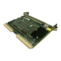
VME Processor Module
Brand: Motorola
|
Category: Control Unit
|
Size: 1.33 MB
Table of Contents
-
-
Introduction25
-
Overview25
-
-
Overview29
-
-
-
Memory Maps30
-
-
-
Uart49
-
-
-
-
Introduction59
-
-
-
PPC Slave65
-
Ppc Fifo67
-
PPC Master68
-
PPC Arbiter73
-
PPC Parity75
-
-
PCI Slave80
-
Pci Fifo84
-
PCI Master84
-
PCI Arbiter92
-
Watchdog Timers100
-
-
MPIC Features108
-
Architecture109
-
-
Timers113
-
Interrupt Router117
-
Reset State120
-
EOI Register121
-
Operation121
-
8259 Mode122
-
Registers123
-
PPC Registers124
-
-
PCI Registers149
-
MPIC Registers162
-
-
-
-
Introduction181
-
Overview181
-
Features181
-
Block Diagrams182
-
-
Performance186
-
Page Holding187
-
SDRAM Speeds187
-
Rom/Flash Speeds190
-
Cache Coherency194
-
L2 Cache Support194
-
Cycle Types195
-
Ecc195
-
Error Reporting195
-
Error Logging197
-
I2C Interface201
-
I2C Byte Write202
-
I2C Random Read205
-
I2C Page Write209
-
CSR Accesses214
-
Refresh/Scrub214
-
-
CSR Architecture215
-
Register Summary215
-
32-Bit Counter251
-
Tben Register253
-
-
-
-
-
I2C Eeproms256
-
SDRAM Size256
-
ECC Codes266
-
-
-
-
Introduction269
-
Introduction282
-
Pci Arbitration282
-
-
-
-
ISA DMA Channels288
-
Exceptions288
-
Endian Issues291
-
PCI Domain294
-
PCI-Ethernet294
-
Pci-Scsi294
-
PCI-Graphics295
-
-
Vmebus Domain295
-
-
Advertisement

Motorola MVME2400 Series Installation And Use Manual (175 pages)
VME Processor Module
Brand: Motorola
|
Category: Control Unit
|
Size: 1.81 MB
Table of Contents
-
-
Introduction21
-
Description21
-
-
-
-
Overview45
-
-
Switches47
-
-
Bfl (Ds1)48
-
Cpu (Ds2)48
-
Pmc2 (Ds3)48
-
Pmc1 (Ds4)48
-
-
DEBUG Port49
-
PMC Slots51
-
Pmcspan52
-
-
-
Introduction53
-
Features53
-
-
-
Assumptions63
-
SDRAM Memory64
-
Flash Memory68
-
-
-
Introduction79
-
Memory Maps79
-
-
DMA Channels86
-
-
-
Introduction125
-
Pin Assignments125
-
Motorola MVME2400 Series Installation And User Manual (20 pages)
Brand: Motorola
|
Category: Single board computers
|
Size: 0.05 MB
Advertisement