
Related Manuals for Motorola MBX Series


Summary of Contents for Motorola MBX Series
- Page 1 MBX Series Embedded Controller Version B Installation and Use MBXA/IH3 September 2000 Edition...
- Page 2 © Copyright 1997–2000 Motorola, Inc. All rights reserved. Printed in the United States of America. Motorola, the Motorola logo, and PowerQUICC are registered trademarks of Motorola, Inc. PowerPC is a registered trademark of International Business Machines Corporation and is used by Motorola with permission.
- Page 3 The safety precautions listed below represent warnings of certain dangers of which Motorola is aware. You, as the user of the product, should follow these warnings and all other safety precautions necessary for the safe operation of the equipment in your operating environment.
- Page 4 Flammability All Motorola PWBs (printed wiring boards) are manufactured with a flammability rating of 94V-0 by UL-recognized manufacturers. EMI Caution This equipment generates, uses and can radiate electromagnetic energy. It Caution may cause or be susceptible to electromagnetic interference (EMI) if not installed and used with adequate EMI protection.
- Page 5 While reasonable efforts have been made to assure the accuracy of this document, Motorola, Inc. assumes no liability resulting from any omissions in this document, or from the use of the information obtained therein. Motorola reserves the right to revise this document and to make changes from time to time in the content hereof without obligation of Motorola to notify any person of such revision or changes.
- Page 6 If the documentation contained herein is supplied, directly or indirectly, to the U.S. Government, the following notice shall apply unless otherwise agreed to in writing by Motorola, Inc. Use, duplication, or disclosure by the Government is subject to restrictions as set forth in subparagraph (b)(3) of the Rights in Technical Data clause at DFARS 252.227-7013 (Nov.
-
Page 7: Table Of Contents
Contents About This Manual Summary of Changes ....................xvii Overview of Contents ....................xvii Comments and Suggestions ................... xviii Conventions Used in This Manual ................. xviii CHAPTER 1 Installation Procedures Equipment Required ....................1-1 Overview of the Installation Procedure ..............1-1 Unpacking the Board ....................1-2 ESD Precautions .................... - Page 8 CHAPTER 4 VPD and ENV Commands VPD—Display Vital Product Data ................4-1 ENV—Set Environment ................... 4-2 CHAPTER 5 Functional Description MBX Block Diagrams ....................5-1 MBX Features Summary ..................5-5 MBX Features Description ..................5-6 General Description ................... 5-6 Processor ......................5-7 MPC860 .....................
- Page 9 CHAPTER 6 Jumpers, Connectors, and LEDs MBX821/860 Connectors, Headers, LEDs .............. 6-1 MBX Jumper Headers ....................6-3 Jumper Settings in Brief ..................6-3 J1 Backup Power Configuration ............... 6-4 J3 Boot ROM Write Protection ................. 6-5 J4 Boot ROM Device Selection ................ 6-6 J5 Test/Debug Port Selection ................
- Page 10 APPENDIX B Related Documentation Motorola Computer Group Documents ..............B-1 Manufacturers’ Documents ..................B-2 Related Specifications ..................... B-3...
- Page 11 List of Figures Figure 5-1. MBX821 Entry-Level Features Block Diagram ........5-2 Figure 5-2. MBX860 Entry-Level Features Block Diagram ........5-3 Figure 5-3. MBX821/860 Standard Features Block Diagram ........ 5-4 Figure 6-1. MBX821/860 Connectors, Headers, LEDs .......... 6-2...
- Page 13 List of Tables Table 1-1. Installation Overview ................1-1 Table 3-1. Debugger Commands ................3-4 Table 5-1. Features of the MBX Series Embedded Controller ....... 5-5 Table 5-2. Fuse Assignments ................5-20 Table 6-1. Jumper Settings ..................6-3 Table 6-2. Power Connector Pin Assignments ............6-12 Table 6-3.
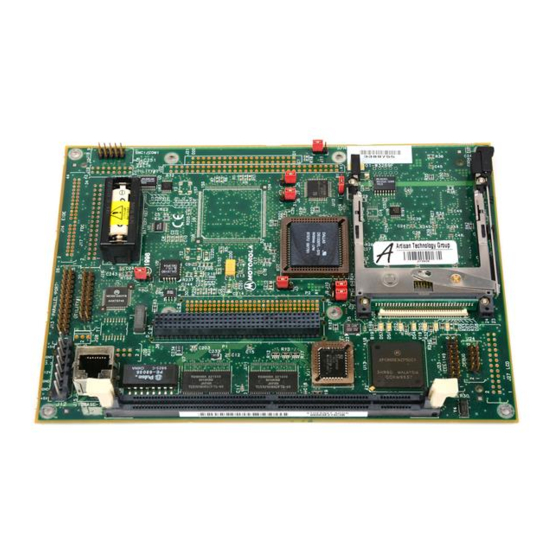
- Page 15 About This Manual The MBX Series Embedded Controller Version B Installation and Use manual provides general information, hardware preparation and installation instructions, operating instructions, a functional description, and various types of interfacing information for the MBX family of embedded controller boards.
- Page 16 MBX821-00x, MBX860-00x MBX Series Embedded Controller Installation and Use (MBXA/IH1) MBX821-00xA, MBX860-00xA MBX Series Embedded Controller Installation and Use (MBXA/IH1) and MBX Series version A customer letter (MBXA/LT1) MBX860-00xC MBX Series Embedded Controller Version C Installation and Use (MBXCA/IH) This manual is intended for anyone who wants to supply OEM systems, add capability to an existing compatible system, or work in a lab environment for experimental purposes.
-
Page 17: Summary Of Changes
Summary of Changes This manual has been revised and replaces previous revisions. Date Changes Replaces 5/00 Updated safety information and legal notices; MBXA/IH2.1 revised the title to reflect covered MBX version 11/98 An important note regarding 5V and 3.3V MBXA/IH2 supplies was added to Power Requirements on page A-2... -
Page 18: Comments And Suggestions
Comments and Suggestions Motorola welcomes and appreciates your comments on its documentation. We want to know what you think about our manuals and how we can make them better. Mail comments to:... - Page 19 italic is used for names of variables to which you assign values. Italic is also used for comments in screen displays and examples, and to introduce new terms. courier is used for system output (for example, screen displays, reports), examples, and system prompts. <Enter>, <Return>...
-
Page 21: Equipment Required
1Installation Procedures This chapter describes the equipment you need and the tasks you will perform to complete an MBX system. Equipment Required To complete an MBX system, you need the following equipment: Enclosure or chassis with power supply Display console Operating system (and/or application software) Disk drives (and/or other I/O) and connecting cables Overview of the Installation Procedure... -
Page 22: Unpacking The Board
Appendix B, Related Documentation Unpacking the Board ESD Precautions Motorola strongly recommends that you use an antistatic wrist strap and a Use ESD conductive foam pad when installing or upgrading a system. Electronic components, such as disk drives, computer boards, and memory modules, can be extremely sensitive to electrostatic discharge (ESD). -
Page 23: Unpacking Guidelines
Preparing the Board for Installation The MBX series embedded controller provides software control over many options. By setting bits in control registers after installing the board in a system, you can modify its configuration. (Control registers are described in the MBX Series Embedded Controller Version B Programmer’s... - Page 24 Installation Procedures begin. Similarly, if you intend to connect an external battery to power the keep-alive circuits on the MBX, you should do so at the time you install the MBX board (see Connecting an External Battery on page 1-10 instructions).
- Page 25 4. If the MBX board-to-chassis standoffs are not already installed in the enclosure, insert the standoffs through the holes drilled for that purpose in the chassis. Secure the standoffs with the nut driver or screwdriver as appropriate. 5. Place the MBX board on the standoffs. http://www.motorola.com/computer/literature...
- Page 26 Installation Procedures 6. Insert four short Phillips screws through the holes at the corners of the MBX board, into the standoffs you installed in the chassis, as shown in the following illustration. Tighten the screws. 2155 9802 7. Connect the power and peripheral cables to the MBX board as appropriate for your system configuration.
-
Page 27: Installing Expansion Modules
No tools are necessary for this procedure, except those needed to remove chassis or system cover(s). Notes 1. If you add an 8xx/COMM expansion module (user-supplied), it must be installed first; PC/104 and PC/104-Plus modules http://www.motorola.com/computer/literature... - Page 28 Installation Procedures stack on top of it. You can stack up to four expansion modules on the MBX. 2. Before mounting expansion modules, ensure that all user- configurable jumpers on the board are set as necessary for your application. Some jumper headers may not be accessible with expansion modules installed.
- Page 29 Note PCMCIA modules can be installed with power applied to the system. Other modules cannot. 4. Seat the expansion module firmly and evenly in the appropriate connector(s) as shown in the following illustration. The plug on the http://www.motorola.com/computer/literature...
-
Page 30: Connecting An External Battery
Installation Procedures underside of the expansion module should connect smoothly with the corresponding socket on the MBX board. 2154 9802 5. Replace the chassis or system cover(s) and reconnect the system to the AC or DC power source as necessary, or proceed to Installing the Board on page 1-3. - Page 31 The ESD strap must be secured to your wrist and to ground throughout the procedure. Wrist Strap 1. While an external battery can be connected with power applied to the system, we recommend that you perform a system shutdown and http://www.motorola.com/computer/literature 1-11...
-
Page 32: Adding Dram
Installation Procedures disconnect the AC or DC power source before connecting an external battery except where necessary to prevent data loss. 2. Connect the external battery to utility connector J16 using an appropriate user-supplied connector. (See Utility Connector J16 on page 6-21 for pinout information.) 3. - Page 33 2. Insert the desired DRAM DIMM into XU3 and secure the DIMM with the clips at each end of the socket. 3. Configure jumper headers J8, J9, and J10 to match the size of the DRAM module as shown in the following illustration. These jumpers http://www.motorola.com/computer/literature 1-13...
-
Page 34: Replacing Lithium Batteries
Installation Procedures specify the address width appropriate for the amount of expansion memory installed. (factory configuration) 16MB 32MB 64MB/ 128MB 2152 9805 (i) Replacing Lithium Batteries Follow these safety rules for proper battery operation and to reduce equipment and personal injury hazards when handling lithium batteries. Use the battery for its intended application only. - Page 35 The ESD strap must be secured to your wrist and to ground throughout the procedure. Wrist Strap 1. To remove the battery from the module, carefully pull the battery from the socket. 2. Before installing a new battery, ensure that the battery pins are clean. http://www.motorola.com/computer/literature 1-15...
- Page 36 Installation Procedures 3. Note the battery polarity and press the new battery into the socket. Note When the battery is in the socket, no soldering is required. 4. Recycle or dispose of the old battery according to local regulations and manufacturer’s instructions.
-
Page 37: Pre-Startup Check
2Startup and Operation Pre-Startup Check Before you power up the MBX system, be sure that the following conditions exist: Jumpers and/or configuration switches on the MBX and associated equipment are set as required for your application. The EPPCBug boot ROM is known to be present in socket XU1 on the top side of the MBX board (if booting from the socketed device);... -
Page 38: Initialization Process
Startup and Operation defaults. In most cases there is no need to modify the firmware configuration before you boot the operating system. For further information on the firmware, refer to Chapter 3, EPPCBug Firmware, or to the EPPCBug Firmware Package User’s Manual listed in Appendix B, Related Documentation. -
Page 39: Restarting The System
Reset Powering up the MBX Series board initiates a system reset. Resets can also be asserted through the Reset switch, available remotely via utility connector #1 (J16 on the MBX board). Both “cold” and “warm” reset modes are available. -
Page 40: Break
Documentation). This machine state is then accessible to you for diagnostic purposes. For details on the firmware or the programming aspects of the MBX series embedded controller, refer to the EPPCBug Firmware Package User’s Manual or to the MBX Series Embedded Controller Version B Programmer’s Reference Guide respectively. -
Page 41: Firmware Overview
A set of command-driven diagnostics, which is hereafter referred to as “the diagnostics.” A user interface which accepts commands from the system console terminal. EPPCBug is similar to previous Motorola firmware debugging packages (e.g., MVME147Bug, MVME167Bug, MVME187Bug, PPCBug), with differences due to microprocessor architectures. These are primarily... -
Page 42: Firmware Implementation And Memory Requirements
EPPCBug Firmware reflected in the instruction mnemonics, register displays, addressing modes of the assembler/ disassembler, and the passing of arguments to the system calls. Firmware Implementation and Memory Requirements EPPCBug requires a total of 512KB of read/write memory (i.e., DRAM). The debugger allocates this space from the top of memory. -
Page 43: Debugger Commands
EPPCBug Firmware Package User’s Manual listed in Appendix B, Related Documentation. Note You can list all the available debugger commands from the command line by entering the Help (HE) command alone. You http://www.motorola.com/computer/literature... -
Page 44: Table 3-1. Debugger Commands
EPPCBug Firmware can view the syntax for a particular command by entering HE and the command mnemonic, as listed below. Table 3-1. Debugger Commands Command Description One Line Assembler Block of Memory Compare Block of Memory Fill Block of Memory Initialize Block of Memory Move BR/NOBR Breakpoint Insert/Delete... - Page 45 MPC8xx Memory Map Display Memory Map Diagnostic Memory Set Memory Write NIOC Network I/O Control NIOP Network I/O Physical NIOT Network I/O Teach (Configuration) NPING Network Ping Offset Registers Display/Modify PA/NOPA Printer Attach/Detach PF/NOPF Port Format/Detach PFLASH Program Flash Memory Program Load http://www.motorola.com/computer/literature...
- Page 46 EPPCBug Firmware Table 3-1. Debugger Commands (continued) Command Description Program Load and Halt Register Display RESET Cold/Warm Reset Read Loop Register Modify Register Set Switch Directories Set Time and Date SYM/NOSYM Symbol Table Attach/Detach SYMS Symbol Table Display/Search Trace Terminal Attach TIME Display Time and Date Transparent Mode...
-
Page 47: Vpd-Display Vital Product Data
4VPD and ENV Commands Two common tasks for which you need the factory-installed debug monitor, EPPCBug, are: Using the EPPCBug command VPD to view board-specific information that is stored in the VPD (Vital Product Data) EPROM on the MBX board. Using the EPPCBug command ENV to edit configurable EPPCBug parameters in the MBX board’s NVRAM. -
Page 48: Env-Set Environment
EPPCBug operational parameters that are kept in NVRAM. Refer to the EPPCBug Firmware Package User’s Manual for a description of the use of ENV. Additional information on registers in MBX series boards that affect these parameters can be found in the MBX Series Embedded Controller Version B Programmer’s Reference Guide. - Page 49 The default value produces a startup delay of five seconds. Program Intermediate Load Address = 00200000? Defines the address in memory where the PL command initially loads the program image. Once the image is loaded at the intermediate load http://www.motorola.com/computer/literature...
- Page 50 VPD and ENV Commands address, its contents are evaluated and repositioned in memory as appropriate for the load image type (ELF, ROMBOOT, or binary). Binary Program Load Address = 00080000? Defines the address to which binary images are moved for execution. Binary images are distinct from ELF or ROMBOOT images.
-
Page 51: Mbx Block Diagrams
5Functional Description This chapter provides an overview of the MBX series embedded controller including a detailed description of the board’s major components. Detailed descriptions of other MBX blocks, including programmable registers in the ASICs and peripheral chips, can be found in the MBX Programmer’s Reference Guide (listed in... -
Page 52: Figure 5-1. Mbx821 Entry-Level Features Block Diagram
Functional Description PPORT Host/Peripherial Population Parallel Port Option MPC821 Debug Port PIP (SMC2, SPI, TDM) IEEE1149.1 Test Access Port SCC2, SMC1, SCC2, SMC1, Ethernet Interface SCC1 I C, CLOCKs, TDM I C, CLOCKs, TDM 10BaseT & AUI PCMCIA INFC CNTL Single Slot PCMCIA Interface... -
Page 53: Figure 5-2. Mbx860 Entry-Level Features Block Diagram
Local Bus & SMC1, SMC2, SPI, I C SMC1, SMC2, SPI, I C, Interface Interface TDM Signals/Clocks TDM Signals/Clocks SMC1 COM1 Devices: Selector EPROM, EIA-232 DIMM, Transceiver To/From Standard Version 2143 9802 Figure 5-2. MBX860 Entry-Level Features Block Diagram http://www.motorola.com/computer/literature... -
Page 54: Figure 5-3. Mbx821/860 Standard Features Block Diagram
Functional Description To/From Entry Level Version 8259INT# QSINT# PC/104- Plus INFC QSPAN / PCI PCI Local Bus QSPAN / REG 83C553 WINBOND ARBITER PCI-to-ISA PCI-to-EIDE BRIDGE INTERFACE CNTLR Power - 1x3 IDE HDR - 2x22 ISA Bus PC/104 INFC 37C672 Peripheral I/O Controller FDC HDR - 2x17 CNTLR... -
Page 55: Mbx Features Summary
MBX Features Summary MBX Features Summary The following table summarizes the key features of MBX series boards. Features pertaining to both entry-level and standard configurations are listed in the upper section. Additional features offered only in the standard configuration are listed in the lower section. -
Page 56: Mbx Features Description
The following topics provide detailed information about the MBX series embedded controller and its principal components. General Description MBX series boards are based on the EBX (5.75" × 8") industry-standard form factor specification. MBX boards provide single-board computer functionality with emphasis on open communications and networking capabilities. -
Page 57: Processor
The MBX series has two branches: one is based on Motorola’s MPC821 embedded processor, the other uses an MPC860 processor. MBX860 models offer four serial communications controllers (SCCs); MBX821 models have two SCCs and an integrated LCD controller. -
Page 58: Mpc821
MBX). The MPC821 also incorporates an LCD controller for display capability. Real-Time Clock/Timer Functions The processor chip used on MBX series embedded controllers incorporates a clock module to provide the various system clock and timer functions as well as low power control circuitry for the system. Among the outputs of the clock module is a real-time clock (RTC). -
Page 59: Dram
MPC821/MPC860 processor user’s manuals. DRAM The MBX series embedded controller has provision for either 4MB or 16MB of on-board DRAM, soldered in place. In addition, it accommodates 8MB to 128MB of expansion DRAM in a 168-pin DIMM (dual in-line memory module) socket, XU3. -
Page 60: Flash Memory
RAS refresh. Flash Memory Flash memory on the MBX series embedded controller consists of 2MB, 4MB, or 8MB of memory in one bank of four devices soldered directly to the board. The EPPCBug firmware resident in Flash memory is originally loaded at the factory, but the Flash contents can be reprogrammed if necessary. -
Page 61: Nvram
NVRAM NVRAM The MBX series embedded controller accommodates 32KB of Non- Volatile RAM (NVRAM) in a 34-pin socket, XU2. A battery within the device supplies VCC to the NVRAM when main power is removed. The NVRAM provides for a low-battery indication which can be read by the processor (via status register #2—see the MBX Programmer’s Reference... -
Page 62: Switches And Status Indicators
Functional Description disconnecting power to the board. You can then replace the jumper and store the board. The freshness seal protecting the on-board battery is automatically broken when you apply power to the board with a jumper on J1 pins 1 and 2. If your application does not use the integrated real-time clock, battery backup is not needed and the on-board battery can be removed. -
Page 63: Status Indicators
The Reset signal on utility connector #1 (J16) is routed to this circuit. Peripheral I/O Controller The MBX series embedded controller uses a 37C672 multi-function I/O controller chip from Standard Microsystems to implement the on-board peripheral functions of the standard version, namely, an asynchronous... -
Page 64: Parallel Port
I/O controller, they use SMC1 on the processor by default. You can also select one port or the other by setting control bits in control register #1 (refer to the MBX Series Embedded Controller Version B Programmer’s Reference Guide for details). -
Page 65: 2.88Mb Floppy Disk Drive Controller
AUI and 10BaseT connections, but you can also select AUI or 10BaseT by setting control bits in control register #1. Every MBX series embedded controller is assigned an Ethernet station address. The address is $08003Exxxxxx, where xxxxxx is the unique six- nibble number assigned to the board (i.e., every board has a different value... -
Page 66: Pcmcia Interface
MBX Series Embedded Controller Version B Programmer’s Reference Guide. PCMCIA Interface A key feature of the MBX series embedded controller is the PCMCIA bus incorporated into the MPC8xx processor chip. PCMCIA modules offer a variety of possibilities for memory expansion and mass storage in addition to networking applications, wireless communications, and industrial I/O. -
Page 67: Mpc8Xx Serial Communications Interface
Portable Systems Microprocessor User’s Manual for detailed programming information. MPC8 xx Serial Communications Interface The MPC8xx processor chip used on MBX series embedded controllers has a versatile communications interface with Time Slot Allocator (TSA) and Time Division Multiplexing (TDM) channels to support multiplexed as well as non-multiplexed serial I/O. -
Page 68: Mpc8Xx Bus Interface
Series Embedded Controller Version B Programmer’s Reference Guide or to the MPC821/MPC860 processor user’s manuals as applicable. PCI/ISA Interface A significant feature of the MBX series embedded controller is the PC/104-Plus interface, derived from the PCI QSpan device (see Figure on page 5-4). -
Page 69: Pci/Isa Bridge Controller
Guide and to the user documentation for the modules you intend to use. PCI/ISA Bridge Controller The MBX series embedded controller uses a Winbond W83C553F bridge controller to supply the interface between the PCI local bus and the ISA system I/O bus (diagrammed in Figure on page 5-4). -
Page 70: Polyswitches (Self-Resetting Fuses)
Polyswitches (Self-resetting Fuses) The MBX series embedded controller draws +3.3Vdc, +5Vdc, and +12Vdc power through power connector header J12. The +5Vdc power is fused on board at its entry to the keyboard and mouse supply circuitry. The +12Vdc power is fused on board at its entry to the LAN circuits on the MBX. -
Page 71: Mbx821/860 Connectors, Headers, Leds
6Jumpers, Connectors, and LEDs In this chapter, you will find information about MBX jumpers and jumper settings, connectors and connector pin assignments, and the on-board LED status indicators. MBX821/860 Connectors, Headers, LEDs The following figure illustrates the location of the jumper headers, connectors, and LED indicators on the MBX board. -
Page 72: Figure 6-1. Mbx821/860 Connectors, Headers, Leds
Jumpers, Connectors, and LEDs XBT1 15 16 J6 J7 J5 J8 J9 J10 XJ26 (MBX821) 2145 9802 Figure 6-1. MBX821/860 Connectors, Headers, LEDs Computer Group Literature Center Web Site... -
Page 73: Mbx Jumper Headers
Arbitration mode External arbitration selected (for one or two external masters). [2-3] Internal arbitration selected (for one external master only). IDE interface “Native” (EIDE) addressing mode selected for IDE configuration interface. [2-3] “Legacy” addressing mode selected for IDE interface. http://www.motorola.com/computer/literature... -
Page 74: J1 Backup Power Configuration
PCMCIA module DREQ# signal on BVD2_SPKR type PCMCIA pin. cards Note MBX series embedded controllers are factory tested and shipped with the default configurations listed above. The MBX family’s required and factory-installed debug monitor, EPPCBug, operates with those factory settings. J1 Backup Power Configuration MBX series embedded controllers can use 3.0V–3.6V battery power... -
Page 75: J3 Boot Rom Write Protection
2146 9802 J3 Boot ROM Write Protection Flash memory on the MBX series embedded controller consists of one bank of four 32-pin PLCC Flash devices soldered directly to the board. Flash memory provides 2MB (in entry-level versions) or 4MB (in standard versions) of storage. -
Page 76: J4 Boot Rom Device Selection
(boot ROM device selection) on the board as well. J4 Boot ROM Device Selection The firmware resident in Flash memory on the MBX series embedded controller is originally loaded at the factory, but the Flash contents can be reprogrammed if necessary. For purposes of reprogramming Flash, the MBX includes a 32-pin socket (XU1) in which firmware programmers can install a removable boot ROM device. -
Page 77: J5 Test/Debug Port Selection
J5 Test/Debug Port Selection Certain MPC821 and MPC860 signal lines have a dual function on the MBX series embedded controller: they may serve either as IEEE 1149 test port signals or as Debug port signals, as illustrated in this table. -
Page 78: J6 Arbitration Mode
Debug Port Header J24 on page 6-13. For additional details on the configuration and use of the multiplexed IEEE 1149 test port and Debug port signals, refer to the MBX Series Embedded Controller Version B Programmer’s Reference Guide (listed in Appendix B, Related Documentation). -
Page 79: J7 Ide Interface Configuration
IDE) devices use controller registers that are relocatable in I/O space, with interrupt requests mapped to the appropriate registers. Use J7 to configure the IDE interface on MBX series boards as necessary for the devices you have installed. Placing a jumper on J7 pins 1 and 2 configures the IDE interface for native addressing mode. -
Page 80: J8-J10 Dram Dimm Size
Jumpers, Connectors, and LEDs J8–J10 DRAM DIMM Size The MBX series embedded controller provides either 4MB or 16MB of on- board DRAM, soldered in place. In addition, it accommodates 8MB, 16MB, 32MB, 64MB, or 128MB of expansion DRAM in a 168-pin DIMM socket, XU3. - Page 81 For non-DMA cards, place a jumper on J11 pins 2 and 3 to permit use of the BVD2_SPKR signal. The factory configuration uses pins 1 and 2 on J11. DREQ# Signal on INPACK# Pin DREQ# Signal on BVD2_SPKR Pin (factory configuration) 2153 9802 http://www.motorola.com/computer/literature 6-11...
-
Page 82: Mbx Connectors And Pin Assignments
Jumpers, Connectors, and LEDs MBX Connectors and Pin Assignments Power Connector J12 A seven-pin friction lock connector, right angle or straight up, serves as power connector. The pin assignments for the power connector are listed in the following table. Table 6-2. Power Connector Pin Assignments Pin # Voltage +12V... -
Page 83: Test Port Header J23
Test Port Header J23 Test Port Header J23 A 16-pin header (J23 on MBX series boards) provides access to an IEEE 1149 test port. The pin assignments are listed in the following table. Note To enable this port, you must configure jumper header J5 (see Test/Debug Port Selection on page 6-7). -
Page 84: Table 6-5. Debug Port Header Pin Assignments
+3.3V DSDO Parallel I/O Header J13 A 26-pin header (J13 on MBX series boards) provides access to the parallel I/O interface. The pinouts are arranged to permit a direct ribbon cable connection to a standard IEEE P1284-A DB25 female connector. -
Page 85: Serial Port Header J18
4.7KΩ resistors. Serial Port Header J18 A 10-pin header (J18 on MBX series boards) provides access to the EIA- 232 serial I/O interface. The pinouts are arranged to permit a direct ribbon cable connection to a DB9 male connector. The pin assignments are listed in the following table. -
Page 86: Ethernet 10Baset Connector J15
Ethernet AUI Header J20 The optional AUI connection is implemented with a 16-pin header (J20) located on the MBX series board. The pinouts are arranged to permit a direct ribbon cable connection to a DB15 female connector. The pin assignments are listed in the following table. -
Page 87: 8Xx/Comm Expansion Connectors
RD− +12V 8 xx /COMM Expansion Connectors MBX series embedded controllers support EBX form factor expansion modules such as PC/104, PC/104-Plus, and 8xx/COMM modules. On MBX860 boards, the 860/COMM expansion connector (P1), a 144-pin high-density socket, provides the electrical connection for expansion modules. -
Page 88: Table 6-11. 821/Comm Expansion Connector Pin Assignments
Jumpers, Connectors, and LEDs Table 6-10. 860/COMM Expansion Connector Pin Assignments Pin # Row A Row B Row C Row D TEA# L1TCLKb (T4_C8) SCC3TXD B4_T4_C7 SCC3RXD L1RCLKb (T3_C6) SCC3RTS B3_T3_C5 SCC3CTS L1TCLKa (B2_T2_C3) SCC3DCD L1RCLKa (B1_T1_C1) +3.3V SCC4TXD L1RXDa SCC4RXD L1TXDa SCC4RTS... - Page 89 I2CSDA BRCOMM# BDIP# BGCOMM# BURST# RD/WR# Reserved Reserved Reserved Table 6-11. 821/COMM Expansion Connector Pin Assignments Row A Row B Row C Row D RETRY# COMMINT# CLKOUT Unused SPKROUT Unused HRESET# TEA# L1TCLKb (T4_C8) B4_T4_C7 L1RCLKb (T3_C6) B3_T3_C5 http://www.motorola.com/computer/literature 6-19...
- Page 90 Jumpers, Connectors, and LEDs Table 6-11. 821/COMM Expansion Connector Pin Assignments Row A Row B Row C Row D L1TSYNCb L1TCLKa (B2_T2_C3) L1RSYNCb L1RCLKa (B1_T1_C1) +3.3V L1RXDa L1TXDa LCD_AC/OE L1RXDb L1TSYNCa L1TXDb L1RSYNCa L1ST4 +12V L1ST3 SMC1RXD SMC1TXD SMC1SYN SMC2RXD/ +3.3V L1CLKOa SMC2TXD/...
-
Page 91: Utility Connector J16
Utility Connector J16 A 20-pin dual-row header known as “Utility Connector #1” supplies the interface between the MBX series embedded controller and external devices such as status LEDs, Reset and Abort switches, and power sources. The pin assignments for this utility connector are listed in the following table. -
Page 92: Lcd & Spi Connector J27 (Mbx821)
Jumpers, Connectors, and LEDs Notes 1. Power Fail Sense# is intended for input and sends a NMI to the processor when voltage falls below 0.8V. The signal is filtered for noise. 2. +3.3V, +5V, −12V, −5V, and GND should only be used for low-power applications. -
Page 93: Pc/104-Plus (Pci) Expansion Connector P2
SB0# PERR# +3.3V SDONE STOP# +3.3V LOCK# +3.3V TRDY# DEVSEL# FRAME# IRDY# +3.3V AD16 +3.3V C/BE2# AD18 +3.3V AD17 AD21 AD20 AD19 +3.3V AD23 AD22 +3.3V IDSEL0 IDSEL1 IDSEL2 AD24 C/BE3# VI/O IDSEL3 AD26 AD25 AD29 AD28 AD27 http://www.motorola.com/computer/literature 6-23... - Page 94 Jumpers, Connectors, and LEDs Table 6-14. PC/104- Plus Expansion Connector Pin Assignments Pin # Row A Row B Row C Row D AD30 AD31 REQ0# REQ1# VI/O REQ2# GNT0# GNT1# VI/O GNT2# CLK0 CLK1F CLK2 CLK3 INTD# RST# +12V INTA# INTB# INTC# −12V...
-
Page 95: Pc/104 (Isa) Expansion Connector J21/J22
IOCHRDY MEMR# DRQ0 SMEMW# MEMW# DACK5# SA19 SMEMR# DRQ5 SA18 IOW# DACK6# SA17 IOR# SD10 DRQ6 SA16 DACK3# SD11 DACK7# SA15 DRQ3 SD12 DRQ7 SA14 DACK1# SD13 SA13 DRQ1 SD14 MASTER# SA12 REFRESH# SD15 SA11 ISACLK SA10 INT7 http://www.motorola.com/computer/literature 6-25... -
Page 96: Eide Connector J14
A 44-pin dual-row header supplies a connection point for an EIDE (Enhanced IDE) hard disk subsystem. The EIDE header permits a direct ribbon cable connection between the MBX series embedded controller and user-installed 2.5-inch hard disk drives. The pin assignments for the EIDE connector are listed in the following table. - Page 97 EIDE Connector J14 Table 6-16. EIDE Connector Pin Assignments (continued) Pin # Signal Signal Pin # REQA IOW# IOR# CHRDY DACKA# IRQA IOCS16# DIAG# CS0# CS1# ACT# Reserved Note ALE, IOCS16#, and DIAG# are not connected on the MBX board. http://www.motorola.com/computer/literature 6-27...
-
Page 98: Floppy Disk Connector J17
Jumpers, Connectors, and LEDs Floppy Disk Connector J17 A 34-pin dual-row header supplies the interface between the MBX series embedded controller and external floppy disk drives. The pin assignments for the floppy disk drive connector are listed in the following table. -
Page 99: Utility Connector J19
Utility Connector J19 A 16-pin dual-row header known as “Utility Connector #2” supplies the interface between the MBX series embedded controller and external devices such as the keyboard and mouse. This utility connector is only available on standard configurations. The pin assignments for this connector are listed in the following table. -
Page 100: Table 6-19. On-Board Led Status Indicators
Jumpers, Connectors, and LEDs LEDs (DS1–DS8) on board the MBX. The following table describes the function of the on-board LEDs. Table 6-19. On-board LED Status Indicators Status Function at Reset DS3 (green) +3.3Vdc OK; lights when +3.3Vdc power is available on the MBX board. DS1 (green) +5Vdc OK;... -
Page 101: General Specifications
This appendix lists general specifications and power characteristics for MBX series embedded controllers. It also describes cooling requirements and FCC compliance. A complete functional description of the MBX series embedded controller appears in Chapter 5, Functional Description. Specifications for the optional expansion modules can be found in the documentation for those modules. -
Page 102: Power Requirements
Specifications Power Requirements Power requirements for the MBX embedded controller depend on the configuration of the module. You can determine the power requirements specific to your application by adding the appropriate values from the following tables. The first table specifies the minimum power consumption of the standard configuration assuming 16MB of on-board DRAM. -
Page 103: Cooling Requirements
3.78 W Cooling Requirements The Motorola MBX series family of embedded controllers is specified, designed, and tested to operate reliably with an incoming air temperature range from 0° C to 70° C (32° F to 158° F) with forced air cooling of the entire assembly (base board and expansion modules) at a velocity typically achievable by using a 100 CFM axial fan. - Page 104 Specifications and 490 LFM flowing over the module. Less airflow is required to cool the module in environments having lower maximum ambient temperature. Under more favorable thermal conditions, it may be possible to operate the module reliably at higher than 70° C with increased airflow. It is important to note that there are several factors, in addition to the rated CFM of the air mover, which determine the actual volume and speed of air flowing over a module.
-
Page 105: Table B-1. Motorola Computer Group Documents
BRelated Documentation Motorola Computer Group Documents The Motorola publications listed below are referenced in this manual. You can obtain paper or electronic copies of Motorola Computer Group publications by: Contacting your local Motorola sales office Visiting Motorola Computer Group’s World Wide Web literature site, http://www.motorola.com/computer/literature... -
Page 106: Table B-2. Manufacturers' Documents
PowerPC MPC821 Portable Systems Microprocessor User’s Manual MPC821UM PowerPC PowerQUICC MPC860 User’s Manual MPC860UM Literature Distribution Center for Motorola Semiconductor Products Sector Telephone: 1-800-441-2447 FAX: (602) 994-6430 or (303) 675-2150 E-mail: ldcformotorola@hibbertco.com W83C553 Enhanced System I/O Controller with PCI Arbiter (PIB) -
Page 107: Table B-3. Related Specifications
For information visit the EBX Form Factor Overview available at the Motorola Computer Group Web site. The following IEEE specification are available from Institute of Electrical and Electronics Engineers, Inc. Publication and Sales Department 345 East 47th Street New York, NY 10017-... - Page 108 Publication Number PowerPC Microprocessor Common Hardware Reference Platform: TB338/D A System Architecture (CHRP), Version 1.0 Literature Distribution Center for Motorola Semiconductor Products Sector Telephone: 1-800-441-2447 FAX: (602) 994-6430 or (303) 675-2150 E-mail: ldcformotorola@hibbertco.com PowerPC Microprocessor Common Hardware Reference Platform: MPRP-CHRP-01 A System Architecture (CHRP), Version 1.0 is also available from:...
- Page 109 Table B-3. Related Specifications (continued) Document Title and Source Publication Number Interface Between Data Terminal Equipment and Data Circuit- ANSI/EIA-232-D Terminating Equipment Employing Serial Binary Data Interchange Standard (EIA-232-D) Electronic Industries Association Engineering Department 2001 Eye Street, N.W. Washington, D.C. 20006 http://www.motorola.com/computer/literature...
- Page 111 Index Numerics configuration data failure LED 6-30 10BaseT 5-15 features connector (J15), pinouts 6-16 installation 8xx/COMM layout connector (P1), pinouts 6-17 parameters, displaying interface 5-17 preparation module installation boot ROM device configuring 5-10, abort switch 5-12 contents air temperature write protecting analog power break connector (J28), pinouts...
- Page 112 configuring disk interfaces 5-15, 5-19 arbitration mode EIDE connector pinouts 6-26 floppy disk connector pinouts 6-28 battery backup 1-12, 5-12, DMA capability 6-11 baud rate 1-7, documentation, related boot memory 5-10, DRAM boot ROM/Flash write protection configuration 1-13, 6-10 console 1-6, 2-1, 5-14 installation 1-12...
- Page 113 external battery, connecting 1-10 I/O controller 5-13 C (interprocessor-integrated features controller) 5-17 by model IDE addressing modes general description IEEE 1149 test port summary header (J23), pinouts 6-13 firmware 3-1, 5-10 selection command buffer signals delay IEEE 1284 parallel port 5-14 offset header (J13), pinouts...
- Page 114 J23 test port header, pinouts 6-13 J24 debug port header, pinouts 6-13 manual conventions xviii J27 LCD & SPI connector, pinouts 6-22 manufacturers’ documents J28 analog power connector, pinouts 6-12 MBX models jumper settings memory jumpers adding 1-12 J1 backup power configuration 1-12, boot ROM 5-12 configuring 5-10,...
- Page 115 PC/104-Plus programs execution offset connector (P2), pinouts 6-23 loading dimensions 5-18 prompts installation interface 5-18 power consumption QSpan 5-18, stacking 1-8, 5-19 activity LED 6-30 R59 and R68 (fuses) 5-20 arbitration 5-19 real-time clock connector (P2) 5-18 registers, PCI interrupts route control pinouts 6-23 related documentation...
- Page 116 SPI (serial peripheral interface) 5-17 timer functions stacking modules 1-8, 5-19 TSA (time slot allocator) 5-17 standard configuration typeface, meaning of xviii standard features Standard Microsystems (SMC) 37C672 5-13 startup commands unpacking guidelines status indicators 5-13 using debugger suggestions, submitting xviii utility connector #1 (J16), pinouts 6-21...